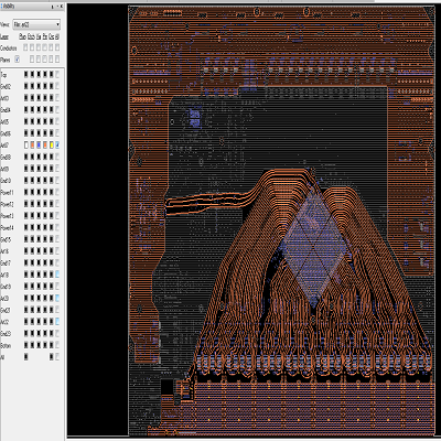
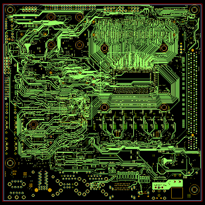
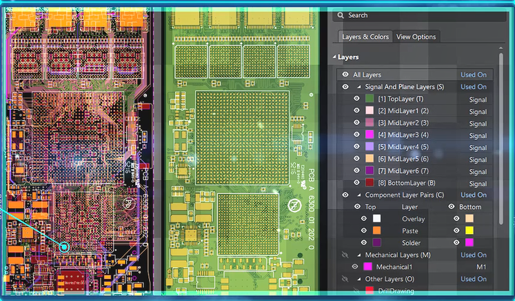
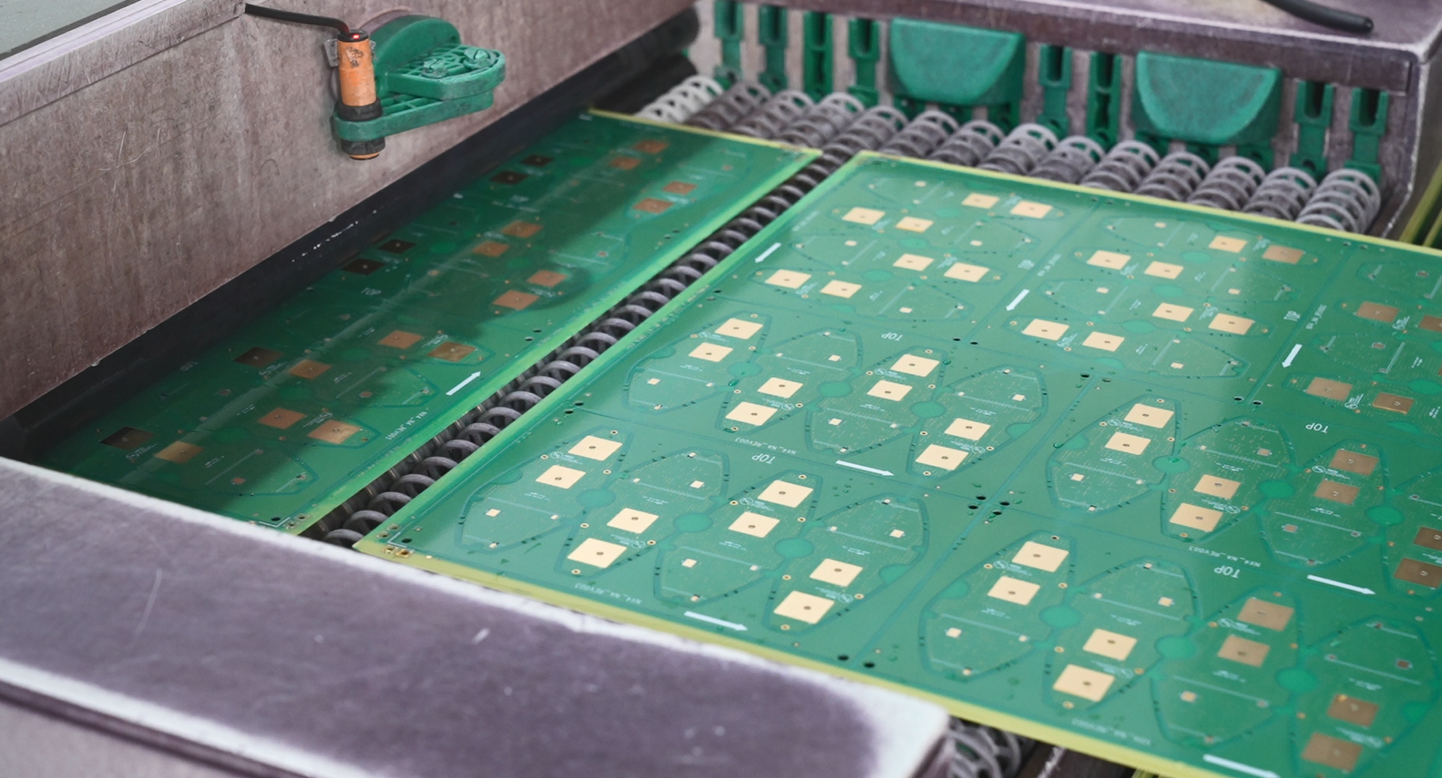
A high-speed circuit handles signals that switch quickly or operate at high frequencies, typically above 50 MHz, though some advanced systems may go into the GHz range. EBest Circuit (Best Technology) is a one-stop PCB manufacturer that covers pcb design, pcb layout, pcb diagram, DFM, SI, PI analysis, PCB manufacturing and so on. In the following, you can see a high speed pcb design solution for industrial switch that we cooperated with our customer.
32 x 400GE industrial switch
[1]: Marvell-400G chip
[2]: 200A maximum current
[3]: Single pair differential line 56G optical network
[4]: 24 layers high power PCB
What’s the Best Material for High-Speed PCB Design?
Choosing the right material is vital for maintaining signal integrity and achieving optimal performance. The material impacts the board’s dielectric constant (Dk), loss tangent, and overall signal quality. Common materials include:
FR4: Widely used but not ideal for very high frequencies due to higher loss tangent.
Rogers (RO4000 series): Preferred for high-speed designs thanks to its low dielectric constant and loss tangent.
Teflon: Excellent for high-frequency applications but more expensive and harder to process.
Selecting the appropriate material ensures the PCB can handle high-speed signals without compromising performance.
For the PCB design service, we can make sure the one-time success to save much time and money for customers. Our goal is to work with customers together and win more market with our clients. Just feel free to contact our technical team if you have similiar designs.
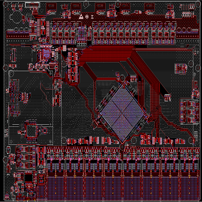
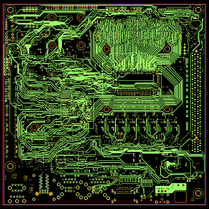
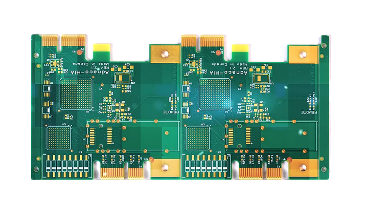
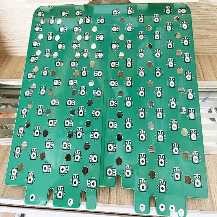
Best technology offers numerous PCB design solutions for our customer, from HDI design, high speed device PCB design, AI optical module design and network motherboard design for network switching. Below is one of our network motherboard design solutions:
An ATCA network switching motherboard
[1]:BCM88XXX, BCM55XXX chips
[2]:60A maximum current
[3]:8口10G optical network
[4]: 8 x DDR3 chips
Network Switching Differential Pair Design Guide
Each TrxP/TrxN signal group (where xcx0-3) shall be routed as a differential pair. This includes the entire length of wiring processing.
The individual differential correspondences are packed together as tightly as possible. Impedance calculations are usually started by selecting the smallest line blank (4-5mil). The tracking width is then adjusted to achieve the necessary impedance.
Differential line group resistance of Ethernet is calculated at 100 ohms.
In general, when routing the four differential pairs of the Gigabit Ethernet to the r45 connector, at least one pair will pass through to the opposite outer layer.
Priority should be given to differential pair wiring. Terminals should be added after the routing is determined
The values of all resistance terminals in the Ethernet front end should be 1.0% tolerance
All capacitor termination Ethernet front ends in the module should have strict tolerances and high quality product media (npo)
You are welcome to contact us if you want to get your DIY network switching PCB designs.
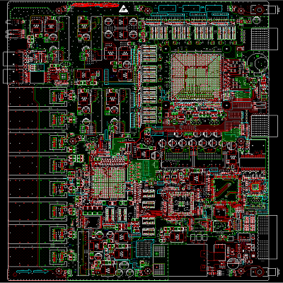
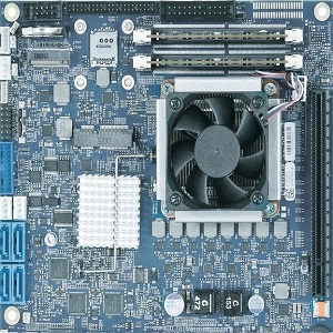
Best technology engaging in the PCB manufacturing and PCB design for more than 17 years. With a strong R&D team, we can provide customers with fast and valued PCB design solutions. Here is one of our industrial motherboard design & industrial PCB case sharing for your reference. If you want to get your own industrial PCB design, welcome to contact us.
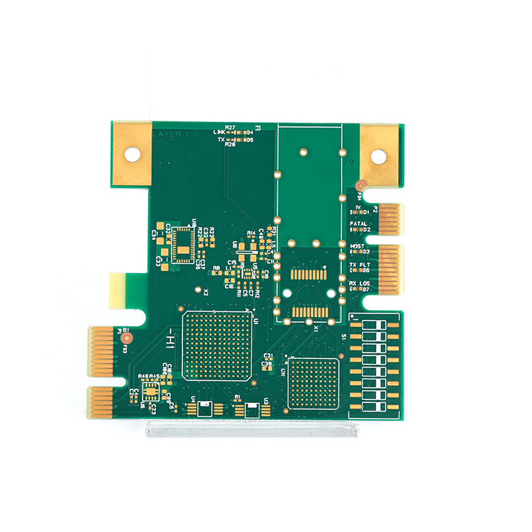
A mITX architecture industrial control motherboard
[5]:2x USB 3.0 (Internal) + 1x USB 3.0 (Client) + 2x USB 3.0 (Rear I/O) + 2x USB 2.0 (Rear I/O) +
2x USB 2.0 (Front Header) + 1x USB 2.0 (mPCIe)
Industrial PCB Design Considerations
Control the length of the circuit: Minimize the length of the circuit, especially the key signal lines, to reduce signal attenuation and delay.
Avoid sharp angles and right angles: Right angles and sharp angles should be avoided when wiring, and rounded or 45 degree angles should be used as far as possible to reduce signal reflection and impedance discontinuity.
Line width: Determine the line width according to the current size and thermal requirements to ensure the reliability and stability of the circuit.
Inter-layer wiring: Rational use of multi-layer PCB inter-layer wiring, such as the signal line on the inner layer, power and ground wire on the outer layer.
Impedance control: For high-speed signals, it is necessary to control the line impedance to ensure signal integrity, and carry out impedance matching design if necessary.
Avoid cross and parallel wiring: Try to avoid cross and parallel wiring of signal lines to reduce crosstalk and electromagnetic interference.
Contact us if you have any questions and inquiry about industrial PCB design projects.
PCB design not only including the routing layout, component placement also is a key parameter. It involves understanding electrical parameters, signal integrity, and thermal management. This article will introduce several golden rules of how to optimize your component placement, whether you are a novice or a seasoned professional, it is helpful for you to manage your circuit board design greatly.
Determine the power supply and grounding plane
In the early stage of PCB design, reasonable power supply and grounding layout is the key. The power supply and ground plane not only provide a stable power supply for the components, but also play a role in reducing electromagnetic interference (EMI). To begin the layout, the first thing is confirming the location of the power supply and ground area. Usually, the power is placed in a complete layer of the PCB, and the ground is in another layer, which can effectively reduce the power supply noise.
Make sure the power plane is close to the area where high power is needed, which can reduce the voltage drops along the supply path. The ground area should be as large and continuous as possible, this helps to provide a good return path and reduce interference from high-frequency signals.
Differentiate layouts by function
When laying out components, dividing the circuit board into different functional areas can improve the efficiency and performance of the design. For example, you can separate power supply into signal processing area, power management area, and interface. This method helps to reduce the mutual interference between different circuits and improve the overall stability of the circuit.
Please noted that, high-frequency components should be close to connectors or key interfaces to shorten the signal path and reduce interference. Low-frequency components can be placed away from critical signal paths to optimize overall signal integrity.
Keep short and direct trace
Shortening the length of signal lines is another important thing to optimize component layout. Make sure keep them short and direct as possible. Long distance signal routing may lead to signal attenuation and delay, which will affect the overall performance of the circuit. Placing the relevant components as close as possible. This not only reduces the length of the circuits, but also reduces the coupling and interference between the signals.
In addition, in the routing process, try to avoid right-angle (90 degrees) turns. Because the right angle will cause signal reflection, affecting the integrity of the signal. Try to use 45 degree turns or arc turns to reduce signal loss.
Consider heat dissipation requirements
Heat management is an important consideration when placing high-power components. Place power components in the edge area of the PCB, such as power transistors and high-frequency converters. This facilitates the use of natural air flow for heat dissipation and convenient for the installation of external cooling devices.
In high-density designs, through-holes, vias and cooling copper blocks can be designed on the PCB, which can transfer heat to the inner layer or bottom of the PCB to help dissipate heat. In addition, maintain a reasonable distance between each component to promote air flow and heat dissipation.
Optimize test points position
Consider placing test points in a convenient location for testing and debugging. Placing test points close to relevant components simplifies the debugging process and reduces test complexity. In particular, the placement of test points on the key signal path can facilitate the detection and verification of signal integrity and stability in the design stage.
For example, the discrete components required for OpAmp operational amplifiers can be placed close to the device, so that the bypass capacitors and resistors can work with them. This helps to optimize the wiring length mentioned as above, while also making testing and fault detection easier.
Consider DFM & DFA factors
Optimizing component layout takes into account not only electrical performance, but also the actual requirements of manufacturing and assembly. For example, try to avoid placing components on both sides of the PCB to simplify the PCBA assembly process. The components are arranged neatly and spaced consistently, which helps the automated assembly equipment to operate efficiently and reduce assembly errors.
Properly using DFM (Design for Manufacturability) principles make production easier and more cost-effective. Ensure that your design can be fabricated with standard processes.
Perform DRC as often as possible
Although it only takes a short time to run DRC (Design Rule Check) functionality on PCB software. But in some complex design environments, perform checks during the design process can save a lot of time, which is a good habit to keep. Every layout routing decision is critical, and running DRC can remind you of the most important layout at any time.
Check production files before sending to manufacturer
While most of PCB manufacturers are happy to download it directly and verify it for you, it is best to export the Gerber file yourself and use the free software such as Gerberv to check that it is as expected to avoid misunderstandings. By verifying it yourself, you may even find some inadvertent errors and thus avoid the cost of completing the production according to the wrong parameters.
[5]:2x USB 3.0 (Internal) + 1x USB 3.0 (Client) + 2x USB 3.0 (Rear I/O) + 2x USB 2.0 (Rear I/O) +
2x USB 2.0 (Front Header) + 1x USB 2.0 (mPCIe)
Anyway, communicating with your manufacturer to understand their equipment and processes can optimize the design, reduce manufacturing problems, improve production efficiency and product quality.
Although semiconductor integration is increasing, many applications have ready-to-use systems on chip. And there are various powerful and out-of-the-box development boards are becoming more readily available, many use cases in electronics still require the use of custom PCBs. In one-time development, even an ordinary PCB can play a very important role. This article will introduce several golden rules of PCB design, and are widely applicable to various PCB design projects.
What are the golden rules of PCB design?
The golden rules of PCB design serve as the foundation for a robust layout. Remember below top 5 rules can help you in PCB designing.
Optimize component placement
Select correct crosstalk
Make sure short and straight circuits
Manage the distribution of power and ground circuit whenever possible.
Avoid sharp angles in traces, opting for 45-degree turns instead.
Additionally, always perform Design Rule Checks (DRC) to catch potential issues before finalizing the layout. These checks help ensure compliance with manufacturing and performance standards.
What are the top 3 important steps in PCB design and layout process?
The PCB design and layout process has many important steps, but these three processes should be given priority.
1. Schematic design and component selection
Start by creating a detailed schematic diagram of your circuit board. As a designer, you can choose discrete components with high or low component values, but with the same performance. By consolidating within a smaller range of standard values, the bill of materials (BOM) can be simplified and potentially cost reduced.
Select suitable components based on the requirements of your design, considering factors like voltage, current, and signal frequency. A clear and precise schematic is essential. It helps avoid errors and streamlines the layout process, making it easier to place and route components effectively.
2. Component placement
Arrange components strategically on the board. Place critical components like microcontrollers and high-frequency ICs first, followed by supporting components. Consider heat dissipation and accessibility for debugging. If you have a range of PCB products based on preferred component values, it will also help you make the right inventory management decisions in the longer term.
3. Routing
Routing including connecting the components with traces. Prioritize routing for critical signals first, such as clock lines and high-speed data paths. Use the shortest possible paths and avoid crossing different signal types to reduce interference. After critical traces, route the power and ground nets, followed by less critical signals. Utilize multiple layers if needed to keep the layout clean and manageable.
What are the guidelines for PCB layout?
PCB layout guidelines can help designers achieve optimal component placement and ensure the board is easy to assemble. Here are some things to consider:
1. Trace width and spacing
Maintain appropriate trace width and spacing based on current carrying capacity and voltage levels. The IPC-2221A standard provides recommendations on PCB trace width and spacing. According to this standard, the trace width must be selected based on current-carrying capacity and permissible temperature rise. For instance, a 1mm wide trace with 1oz. copper (35μm) can carry approximately 2.5A with a 10°C temperature rise.
2. Layer stack-up
Design your PCB stack-up carefully. Multilayer designs are typically used in high-frequency applications to effectively separate power, ground, and signal layers, thereby reducing electromagnetic interference (EMI). Studies show that in a 4-layer or more stack-up, closely coupling the power and ground planes can significantly reduce EMI and improve signal integrity.
3. Thermal management
Consider thermal aspects in your layout. Place components that generate significant heat, such as power transistors, away from heat-sensitive components. Use thermal vias and heat sinks to manage heat dissipation effectively.
4. Via placement
Use vias strategically to connect different layers. Avoid placing too many vias close to high-frequency signal paths to prevent signal degradation. Use via stitching to enhance ground planes and reduce loop areas.
5. Power distribution
Using wide traces for power and ground planes is critical to minimizing resistance and inductance. For instance, IPC-2152 provides guidelines on power distribution and suggests using wide traces to handle higher currents and minimize voltage drops.
What are the considerations of PCB layout?
When designing a printed circuit board, you can consider these points:
1. Signal integrity
Maintain signal integrity by minimizing trace lengths and avoiding impedance mismatches. Use differential pairs for high-speed signals and keep them close together to reduce noise.
2. EMI/EMC
EMI and EMC are critical considerations. Use proper shielding and grounding techniques to mitigate interference and ensure compliance with regulatory standards.
3. Design for Manufacturability (DFM)
Ensure your layout is manufacturable by adhering to fabrication capabilities and tolerances. Simplify routing and avoid excessive component density to facilitate easier assembly and inspection.
4. Mechanical constraints
Consider the physical dimensions and mounting requirements of your PCB. Ensure that components and traces do not interfere with mechanical parts or enclosures.
5. Cost
Optimize your design for cost by reducing layer count where possible and minimizing the use of expensive materials or processes. Balance performance requirements with budget constraints.
At EBest Circuit (Best Technology), we offer expert design services to help you achieve your project goals with precision and excellence. Choose us for your next PCB project and experience the benefits of quality and innovation.
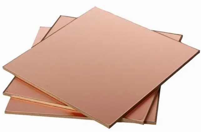
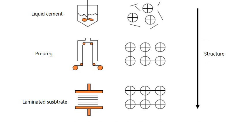
Copper Clad Laminate as a base material of FR4 PCB, serving as a key part in the building of printed circuit board. Understanding what Copper Clad Laminate is, its benefits, types, and manufacturing process is essential for anyone who involved in the electronics industry. This article aims to provide a comprehensive overview of copper clad laminate material, and hope everyone in the PCB industry be interested in it.
What is copper clad laminate?
Copper Clad Laminate, short for CCL, is an electronic glass fiber cloth or other reinforcing material dipped in resin, one or both sides covered with copper foil and made of a plate-like material, referred to as copper clad plate. It also called “Core” when used in the multi-layer PCB designs. Through the different process like etch, drill or copper plating, we can generate different patterns, layouts onto the surface of the CCL, and then form a circuit board that we saw in the electronics.
CCLs provide the necessary support and electrical insulation in an electronic device, while also facilitating the pathways for electrical currents through the copper foil. So, in another word, the performance, long-term reliability and stability of the PCB depend on the CCL to a large extent.
What are the types of copper clad laminates?
Generally speaking, copper clad laminate can be divided into two main types according to its mechanical properties, they are – rigid copper clad laminate and flexible copper clad laminate. Here we listing the detailed types of CCL.
Rigid copper-clad laminate
a. According to different insulation materials and structures: organic resin clad copper laminate, metal clad copper laminate, ceramic clad copper laminate.
b. According to the thickness of the plate: conventional copper-covered laminate and thin copper-covered laminate. The thickness less than 0.5mm (doesn’t include the copper foil) is called thin CCL.
c. According to the reinforcement material used: electronic glass fiber cloth base copper foil board, paper base copper foil board and composite base copper foil board.
d. According to the insulating resin used, such as epoxy resin copper-coated foil board, polyester resin copper-coated foil board and cyanate resin copper-coated foil board.
e. Special rigid copper clad plate, according to the flame-retardant grade and some special properties.
Flexible copper clad laminate
a. polyester types (flame retardant and non-flame retardant)
b. polyimide type (flame retardant, non-flame retardant)
c. Extra thin electronic glass fiber cloth copper foil laminate
What’s the main composition of copper clad laminate?
A normal copper clad laminate mainly consists of copper foil and some auxiliary materials. These materials make the CCL conductive and be used as the core material of the circuit board. Here we would like to explain these compositions in details:
Copper foil
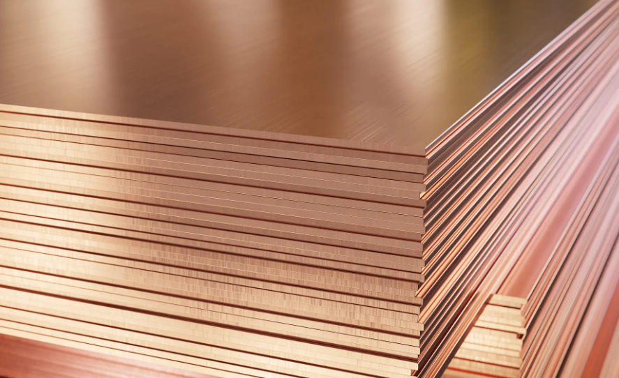
Copper foil is one of the main raw materials for manufacturing copper clad laminate, and it is a very pure metal material with excellent electrical conductivity. The thickness and purity requirements of the copper clad foil are very high, usually between 18-70μm, and the purity is more than 99.8%. In the manufacturing process of CCL, copper foil is used as a conductive layer to transfer current from one electronic component to another. It also has good plasticity and ductility, and can be bent, stretched and formed as needed without adversely affecting electrical conductivity. In addition, the corrosion resistance of the copper foil is also very good, which can resist the erosion of chemical substances, ensuring that the CCL can work properly in a variety of environments.
Auxiliary materials like resin and adhesive
In addition to copper foil and copper clad foil, the production of CCL also involves some other auxiliary materials, such as adhesives and reinforcing materials. Among them, the adhesive is mainly used to fix the copper foil and copper clad foil on the substrate. The selection of adhesives should take into account their adhesion and high temperature resistance to ensure that the copper foil and copper clad foil can be firmly bonded to the substrate. Reinforcement materials are mainly used to improve the mechanical strength and bending resistance of CCL. Common reinforcement materials include glass fiber cloth and polyimide film.
CCL Manufacturing Process
The manufacture of CCL is a meticulous process; therefore, it includes many accurate steps:
Prepare substrate – the commonly used substrate is fiberglass cloth impregnated with epoxy resin, which is non-conductive material and has good insolation and mechanical properties, then cured to get the correct mechanical and thermal characteristics.
Surface treatment – this is a surface cleaning and grinding process to achieve a clean and roughness surface of the substrate, resulting a good adhesion between the copper foil and substrate.
Copper Foil Lamination – lamination of copper foil onto the prepared substrate is done by temperature and pressure quickly and smoothly to obtain a stable bond. This is a lamination process of single layer CCL, if you want a multi-layer CCL, coating adhesive on each layer and then laminate in the press machine, then making them in a whole product.
Cutting and Trimming – the need for the dimensions drives the sheets to be cut and trimmed into a desired size.
Quality Checking: A thorough quality check follows to confirm that the CCL matches industry requirements on thickness, adhesion, and electrical properties.
Where is the Copper Clad Laminate uses?
CCL has a widely applications thus constituting a critical element for numerous electronic devices and systems, the typically are including:
Consumer electronics like cell phones, laptops, and tablets
Automotives including infotainment and engine control units
Industrial equipment like common test equipment
Telecommunications such as networking equipment and communication devices
Medical device, for example: imaging system, diagnostics
If you are looking for a company that can advance and improve your electronic circuit, then EBest Circuit (Best Technology) is the right choice for you. EBest Circuit (Best Technology) is a one-stop solution providers in China with extensive years of experience in high quality PCB and PCBA manufacturing. We have certificated by ISO9001, ISO13485, IATF16949 to make you no worry about the quality. Contact us right now to get your quotations!
In the design of electronic devices and systems, power distribution and heat dissipation management are key factors. Bus bar PCB, as an efficient solution, is particularly outstanding in these aspects. In this article, we would like to introduce the advantages of Bus bar PCB and its applications in different industries.
What Is A Bus Bar PCB?
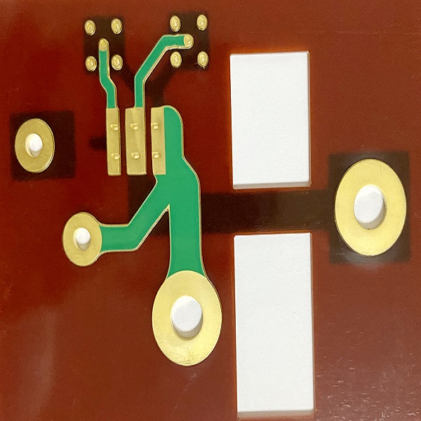
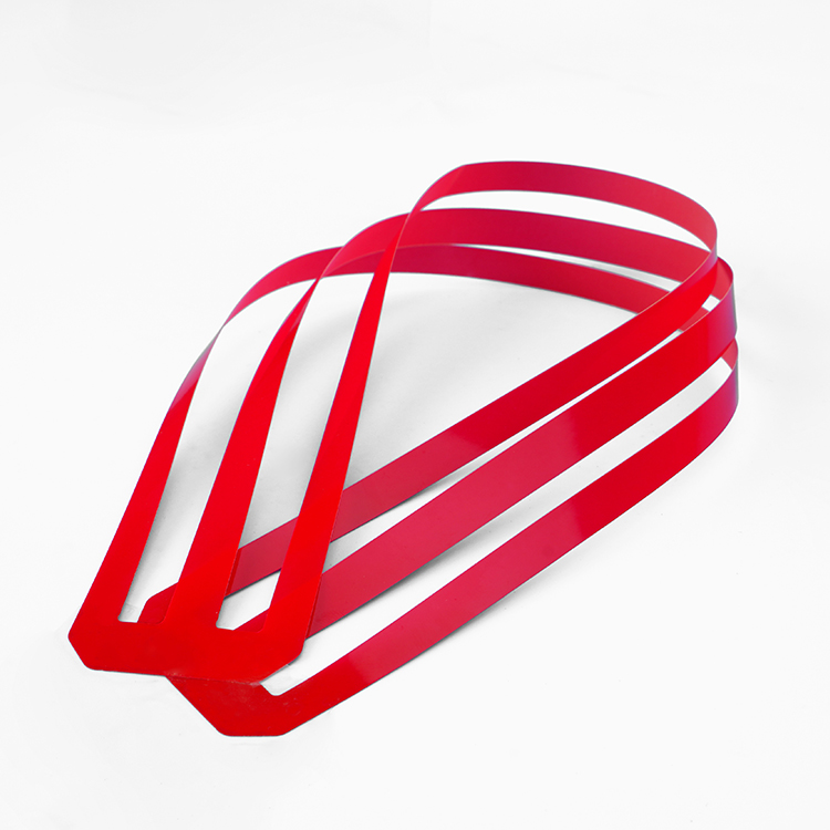
At the beginning, we should know what a bus bar PCB is. The Bus bar PCB is a special and newest design that integrates the FR4 material and metal alloy into a whole product, which allows the current transfer path into the circuit board. Due to the current carry capacity and special shape, it also called busbar PCB, embedded bus bar PCB, extruded copper PCB, copper inlay PCB, copper extrusion PCB.
Bus bar circuit board provide a more compact and efficient means of current distribution than traditional wires and cables. This design improves the overall performance of the electronic system by reducing inductance, increasing current carrying capacity, and optimizing heat dissipation.
What Are the Advantages of Bus Bar PCB?
Bus bar PCB offers numerous benefits when be using the power supply applications, its main functions are:
1. Reduce the inductance
Bus bar PCBs reduce inductance by allowing current to flow between tightly spaced conductors. This layout reduces the loop area and thus the inductance value. This is particularly important for high-frequency and highspeed applications, as it reduces voltage spikes and noise, improving system stability and performance.
2. Enhanced current carrying capacity
Due to its large cross-sectional area and high-quality conductive materials, Bus bar PCB can efficiently carry large currents. This is particularly useful in applications that require a large amount of power distribution, such as power supplies, electric vehicles, and renewable energy systems. Bus bar PCBs support higher current density compared to conventional PCB wiring, which improves thermal management and reliability.
3. Improve thermal management
The Bus bar PCB effectively dissipates heat generated by key components. In high power applications, the buildup of heat can affect performance and life. The Bus bar PCB helps maintain optimal operating temperatures through efficient heat distribution, reducing the need for additional cooling mechanisms.
4. Save space and weight
The compact design of the Bus bar PCB reduces the overall size and weight of the electronic components. Its simple construction and elimination of multiple wire connectors contribute to space savings. This is particularly beneficial for applications where size and weight are critical, such as the aerospace and automotive industries.
5. Improved reliability and durability
Bus bar PCBS have superior mechanical strength and durability compared to traditional wiring systems. Its robust construction and secure connections reduce the risk of loose connections, failure due to vibration, and mechanical wear. This improves system reliability and service life for harsh environments and demanding applications.
6. Simplify assembly and maintenance
Using a Bus bar PCB simplifies the assembly process because it reduces the number of individual wires and connectors. This not only speeds up installation, but also reduces assembly errors. In addition, the Bus bar PCB provides a more orderly and accessible layout for easy troubleshooting and repair.
7. Cost effective
Although there may be a high initial cost, Bus bar PCBs can provide cost savings in the long term. Its advantages in reduced inductance, improved thermal management and enhanced reliability reduce operating and maintenance costs. In addition, Bus bar PCB reduces the need for addons, such as heat sinks or complex wiring bundles, thereby increasing overall cost effectiveness.
What Applications of Bus Bar PCB?
Due the high current carry capacity of the bus bar PCB, makes it very suitable for power supply or power management devices. Bus bar PCB can perform well in such fields. Here are some common application examples that bus bar PCB can be used for. If you are seeking for a PCB to integrate into your power supply project, then bus bar PCB is the go-to-choice.
1. Power Electronics
In power converters, inverters and high-current power supplies, Bus bar PCBS are widely used because of their ability to efficiently handle high currents and excellent thermal performance.
2. The Automobile industry
Another popular field that bus bar PCB used in is automotives, especially in electric vehicles (EVs) and hybrid electric vehicles (HEVs). In the electric cars, it can be used for battery connectivity and power distribution, contributing to weight reduction and performance improvements.
3. Renewable energy
Bus bar PCB is an environment friendly material, it is often used in solar systems, wind turbines and energy storage solutions to manage high currents and enhance reliability.
4. Industrial equipment
In industrial machinery and equipment, Busbar PCB provides powerful and efficient power distribution for motors, drives and control systems.
5. Aerospace
Bus bar PCBS are used in aerospace applications, such as avionics and power distribution systems, where size, weight and reliability are key factors.
Final Words
All in all, bus bar PCB offers significant advantages in handling high currents, improving thermal management, and providing reliable power distribution across various applications. By integrating bus bar PCBs, industries can achieve better power management, reduced system size and weight, and improved overall reliability.
EBest Circuit (Best Technology) is a one-stop PCB solution provider in Asia, we offer various kinds of PCBs not only include bus bar PCB, but also Extra thin PCB, RF PCB, HDI PCB, Heavy copper PCB, Ceramic PCB, Metal Core PCB, Flex PCB and rigid flex PCB, PCBA and so more. We have more than 17 years-experience in PCB design and manufacturing, and served more than 1200 customers. Choosing EBest Circuit (Best Technology) as your supplier ensures you get high quality PCBs, helping to improve the performance and competitiveness of your products. Contact us right now to customize your own PCB!
Gold plating is a common surface finish in PCB manufacturing, also known as nickel gold electroplating. It provides excellent conductivity, corrosion resistance and good durability to electronic devices. However, not all gold plating is created equal. There are two primary types of gold plating are used in PCB fabricating: hard gold plating and soft gold plating. They differ in properties, manufacturing process and applications, let’s explore it today!
What are Hard Gold Plating and Soft Gold Plating?
In the manufacturing process of printed circuit boards (PCBs), we often hear the words “soft gold” and “hard gold”. They are actually describing the different metal materials used in the gold-plating process.
Hard gold usually refers to an alloy formed by electroplating process. This alloy is doped with other metal elements, such as nickel, cobalt, etc., to make it harder and more resistant to friction. Hard gold is especially suitable for places that require force and friction, such as the edge contact points of circuit boards (commonly known as “gold fingers”), because it can withstand frequent insertion and removal operations. Although the processing process of hard gold is complex, it can be doped with other metals to improve the hardness of gold, making it more suitable for making hollow jewelry or for industrial applications.
Soft gold refers to the state of pure gold or close to pure gold, because of the high purity of gold, it is relatively soft. Soft gold is mainly used for aluminum wire on COB (Chip On Board), or the contact surface of mobile phone keys, because it can maintain good electrical conductivity and weldability. The processing process of soft gold is relatively simple, does not require complex alloying process, and maintains the soft characteristics of gold, which is suitable for the production of solid jewelry or for applications requiring good electrical conductivity.
Properties and applications: hard gold plating vs soft gold plating
Hard gold plating is known for its high hardness, typically achieved by alloying gold with small amounts of nickel or cobalt. So, it has highly resistant to wear and mechanical stress. The thickness of hard gold plating is usually greater than that of soft gold plating, ranging from 30 to 50u’’ or more. EBest Circuit (Best Technology) can make up to 50u’’ if you required. Due to the hardness of the hard gold plating, they are commonly used in edge connectors, keypads, and contact points where repeated mechanical action occurs.
The manufacturing process of soft gold plating involves a chemical process to deposit a thinner layer of pure gold onto the PCB surface. The coated pure gold without any alloying elements, resulting in a softer finished compared to the hard gold plating. Additionally, the thickness of soft gold plating is typically thinner than that of hard gold plating, usually around 1 to 3u’’. Due to the softness and conductivity properties, the soft gold plating technology is often used in applications requiring high conductivity and precision, such as wire bonding and fine-pitch components in high-frequency and high-speed circuits.
What’s the difference between gold plating and immersion gold?
Actually, Immersion Gold is mostly called ENIG (electroless nickel immersion gold) surface treatment method. The advantage of this method is that nickel and gold can be attached to copper without electroplating process, and its surface is smoother than gold plating, which is especially important for the shrinking electronic parts and components requiring flatness.
The method of leaching gold is chemical deposition. A coating is formed by chemical redox reaction, which is generally thick. Electroplating gold is based on the principle of electrolysis, also known as electroplating. Most other metal surface treatments are electroplating. In actual product applications, 90% of the gold PCB board is dipped in gold, because the poor weldability of the electric gold-plated board is its fatal defect.
Nickel gold coating with stable color, good brightness, smooth coating and good weldability can be deposited on the surface of printed circuit by gold leaching process. It can be divided into four stages: pretreatment (degreasing, micro-etching, activation, post-leaching), nickel plating, gold leaching, post-treatment (waste gold washing, DI washing, drying). The thickness of gold leaching is 0.025-0.1um. Gold is used in the surface treatment of the circuit board because gold has strong electrical conductivity, good oxidation resistance and long service life. General applications such as keyboard board, gold finger board, etc.
Choosing between hard gold plating and soft gold plating for your PCB depends on your specific application requirements. At EBest Circuit (Best Technology), we offer expert guidance and high-quality PCB manufacturing services to help you select the best surface finish for your needs. Choose us as your trusted PCB supplier to ensure reliable and efficient solutions for all your electronic projects.
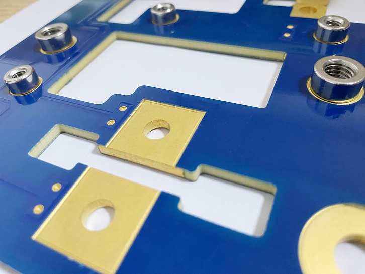
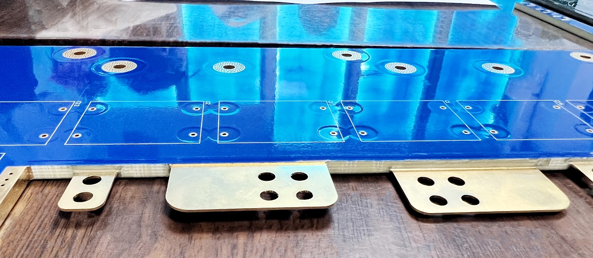
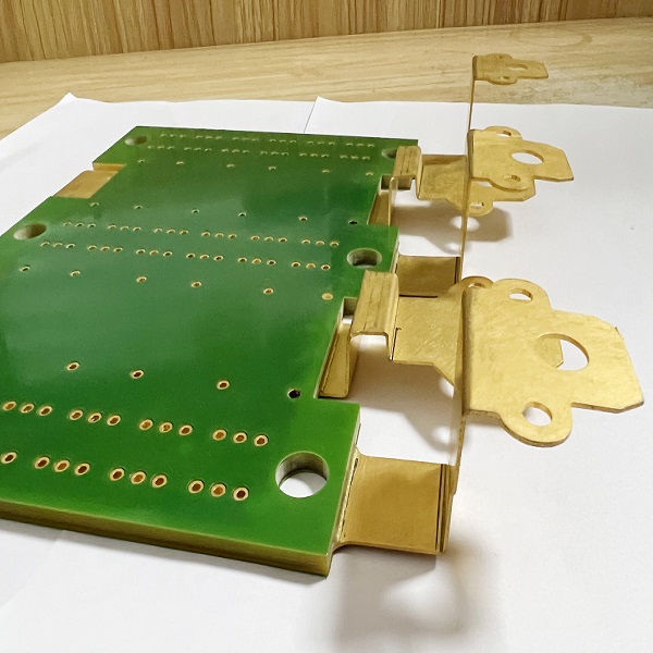
In the electronics industry especially for new-energy vehicles, a Bus Bar PCB plays an important role to achieve specific function. It transmits large amounts of current through metal strips or conductive paths, making it ideal for high-power applications. The design of busbar PCBs is a key technical area for designers or engineers who engaged in power distribution or who require efficient current management. In this article, we would like to share some information about the considerations during a bus bar circuit board designing, hope this may help you to design a desired PCB successfully.
What is a Bus Bar PCB?
Bus bar PCB is one of a new type of heavy copper PCB and it was made by FR4 fiber glass material and laminated with metal alloys. It transmits electrical energy from one point to multiple output points through integrated conductive paths, which are typically made of copper or aluminum. Busbar PCBs are designed to reduce resistance and inductance, thereby maximizing current transfer efficiency and minimizing energy loss.
Generally, if it is used in a charging pile product, there are generally at least 2 busbar circuit boards, one is the main control board (a larger one), and the other is a smaller board, both of two need to use the bus bar process.
Bus bar PCB is widely used in power distribution systems, electric vehicles, industrial equipment and other occasions requiring high current. They are designed to simplify system wiring, reduce electromagnetic interference (EMI), and improve overall reliability and performance of the product.
Why is High Current Bus Bar PCB Important?
Bus bar PCB has irreplaceable advantages in current transmission and power distribution. They mainly feature three functions when used in electronics. First of all, they are able to efficiently handle large currents without generating excessive heat. This is what standard FR4 PCB cannot achieved. Secondly, bus bar PCB has ability to significantly reduce the complexity of the circuit layout design. By integrating the current transfer path, they can reduce the number and length of circuits required by the system, thereby simplifying system design and reducing potential failures.
In addition, bus bar PCB helps reduce electromagnetic interference. Due to the design optimization of the conductive path, the noise generated during current transmission can be effectively suppressed. This characteristic makes it perform well in high-noise environments, ensuring the stability and reliability of electronic devices.
What Should We Consider When Designing A Bus Bar PCB?
Due to it is a new innovation in the industry, it is a not a simple thing to design a bus bar circuit board successfully. It’s a complex task that requires consideration of several technical factors to ensure its effectiveness and reliability. The following are the main aspects to focus on when designing a bus bar PCB.
Copper Thickness
The first important thing is what’s the copper thickness of busbar you want to. You must know, thicker copper allows for higher current carrying capacity, but not thicker thickness is better, it should be calculated according to the voltage and current it will used in.
Current capacity and temperature management
The bus bar PCB should be designed to carry the maximum expected current while keeping the temperature within a safe range. This is usually achieved by selecting the appropriate conductor material and optimizing the cross-sectional area of the conductor. For example, for 100A current requirements, a typical design would use copper strips with a thickness of 5mm to ensure that the temperature rise does not exceed 20C.
Resistance and inductance
Low resistance and low inductance are key to bus bar PCB design. The shape, thickness and layout of conductors should reduce resistance and inductance as much as possible to improve the efficiency of current transmission. For example, the use of trapezoidal or flat conductors can effectively reduce inductance, thereby improving current transmission performance.
Electromagnetic compatibility (EMC)
Bus bar PCB design also needs to consider electromagnetic compatibility issues to ensure that it does not produce too much electromagnetic interference (EMI), while being able to resist external electromagnetic interference. By optimizing the conductor layout and using shielding materials, the electromagnetic compatibility of the bus PCB can be significantly improved.
Thermal management
Because bus bar PCB aims to transmit high current, thermal management is an important part of the design. The thermal design should ensure that the PCB can effectively dissipate heat and prevent overheating damage. For high power applications, radiators or active cooling are often used to ensure temperature control within design specifications.
EBest Circuit (Best Technology) Manufacturing Capability of Bus Bar PCBs
As the one of leading PCB manufacturers in China, EBest Circuit (Best Technology) has exceptional capabilities in the production of busbar PCBs. Our manufacturing capabilities include high-precision metal processing technology to produce busbar PCBs with complex geometry and tight tolerances. In addition, we also have the production capacity of multi-layer bus bar PCB to meet the needs of different applications.
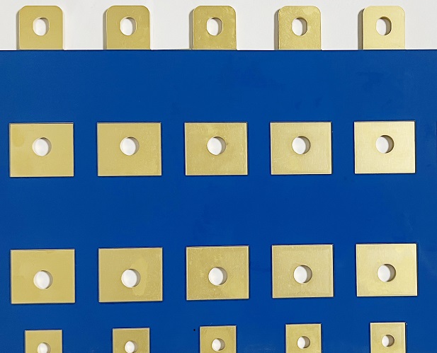
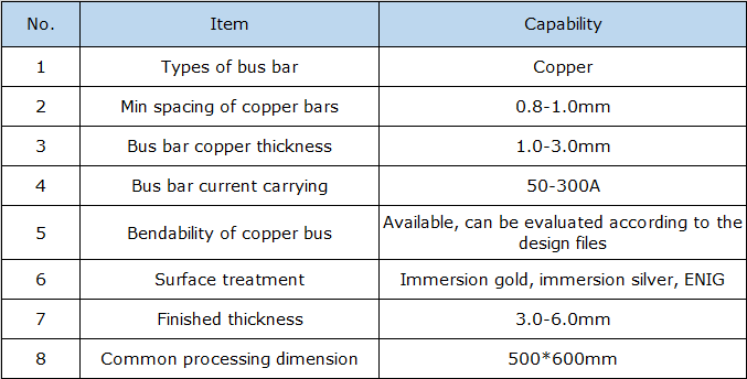
EBest Circuit (Best Technology) is committed to providing customers with high-quality, high-performance busbar PCBs to support their power management and distribution systems. Below is a basic parameter of our bus bar PCB manufacturing capability. For more details, welcome to e-mail us at sales@bestpcbs.com.
(Best technology capability of bus bar pcb)
Nowadays, bus bar PCBs are widely used in power distribution systems, electric vehicles, industrial equipment and other occasions requiring high current. According to statistics, the global busbar market is expected to grow at a compound annual growth rate (CAGR) of 6.5% between 2023 and 2028, demonstrating the growing importance of this technology in multiple industries.
With the rapid development of the eras, the most important thing for designers or buyers is to find a reliable bus bar PCB manufacturer to meet the high demands of the market. As the expert of the bus bar PCB fabricating, EBest Circuit (Best Technology) has the mature technology and advanced equipment to produce high quality bus bar PCBs. Contact us right now to get your own bus bar PCB solutions!
FR4 material is a highly popular and widely used substrate in the PCB industry due to its exceptional mechanical strength, electrical insulation, and flame retardant properties. It has become the standard for PCB fabrication.
What is FR4 Material and Why is it Used in PCBs?
FR4 is a type of fiberglass-reinforced epoxy laminate. The term “FR4” comes from its flame-retardant properties, meeting the UL94V-0 standard. It is made from woven fiberglass cloth and epoxy resin, which together provide great strength and durability.
Electrical engineers and designers prefer FR4 because of its many benefits, such as:
Low cost
High dielectric strength
Excellent strength-to-weight ratio
Moisture resistance
Temperature endurance
Good electric loss characteristics
Flame retardance and self-extinguishing capabilities
Mechanical robustness
Insulating properties
FR4 is also suitable for marine PCBs because it absorbs very little water. In a standard FR4 PCB, a layer of FR4 is placed between two thin layers of laminated copper.
What are the Key Performances of FR4 Material?
FR4 material, also recognized as flame retardant 4, is a composite of glass fabric and epoxy resin, predominantly utilized as a foundational material for printed circuit boards. Familiarity with the specifications of FR4 is crucial for selecting the appropriate substrate for PCB manufacturing. Key specifications include:
1. The thickness of FR4 sheet is usually 0.2 mm to 3.2 mm, and other special thickness also available.
2. The specific gravity of FR4 material is about 1.85g/cm3, which means that it is heavier than water.
3. Coefficient of thermal expansion of FR4 is about 1.0×10^-5cm/cm/℃, which means that its length or width will expand slightly when the temperature changes.
4. The thermal decomposition temperature of FR4 materials is usually between 280C and 320C, which makes it able to withstand high temperature applications.
5. FR4 material has a dielectric constant around 4.0-4.8, which makes it an ideal material for circuit board manufacturing.
6. FR4 has good arc resistance, which means that in the case of high voltage, it can effectively prevent arc discharge.
7. FR4 material good hydrolysis resistance and can maintain good performance even in a humid environment.
What are the Types of PCB Materials in the Industry?
PCB materials can be broadly categorized based on their composition and intended application. Nowadays, the commonly used are including FR4, polyimide (PI), Metal material (copper or aluminum), ceramic substrate like Al2O3, AlN, Si3N4, and so on. Different materials have its unique functions and well-suited in specific environment. Here we introduce their properties and suited applications simply.
FR4 (Fiberglass Epoxy Laminate)
At present, almost of PCB you seen in the market or electronics used the FR4 material. It widely used because of its superb equilibrium of mechanical strength, electrical insulation, and cost-efficiency. Actually, according to the different reinforcement materials, the circuit board is mainly classified into the following types:
1) FR-4
2) FR-1, FR-2, etc.
3) CEM series: Composite substrate
FR-4 used frequently because of its high fire resistance rating.
High Tg FR4
Though normal FR4 material has good electrical insulation, it is not an ideal option for high frequency circuit board. And then, high Tg FR4 stands out by using an advanced technology. “Tg” refers to glass transition temperature, the juncture at which the material transitions from a rigid, glassy state to a pliable, rubbery state. High Tg FR4 boasts a Tg of 170°C or higher.
Polyimide (PI)
Polyimide materials are renowned for their excellent flexibility, superior thermal stability and chemical resistance. It is always used as raw material of flex circuits, rigid flex circuit boards or membrane switches. Due to the good chemistry properties, they can endure temperatures up to 260°C and are highly flexible, making them ideal for those small and limited PCB designs.
Metal base material
Metal materials always used in metal core PCBs (MCPCB), usually used aluminum core or copper core. The metal base has great thermal conductivity to enhance the thermal management of the device, buy using metal core, the device can dissipate heat away from the critical component such as LED chips, ICs, BGAs, to remain the reliability and performance of the PCB.
Ceramic substrate
Ceramic PCB substrate offers excellent thermal conductivity and stability than that metal core PCBs, making them suitable for high-power and high-frequency applications. But due to the high cost and complex manufacturing, the ceramic PCB is much expensive than metal core PCB, therefore, they are always be used in high-end applications, such as the military, defense, aerospace and some special fields where requires excellent thermal management.
Understanding these materials enable to help engineers and designers in selecting the most appropriate substrate for their projects, ensuring optimal performance and cost-efficiency. EBest Circuit (Best Technology) provides a comprehensive array of PCB materials, guaranteeing high-quality solutions for all your electronic needs.
What are the Applications of FR4 PCB Material in Various Industries?
FR4 material is versatile and finds applications in numerous industries, including:
Consumer Electronics like smartphones, laptops, and other personal electronic devices.
Applied in vehicle electronics for infotainment systems, engine control units, and more.
Industrial Equipment such as control systems, power supplies, and industrial automation.
Essential for telecommunications, network devices, routers, and communication infrastructure.
Medical instrumentation and diagnostic equipment.
Aerospace and defense in avionics, radar systems, and defense electronics.
This is all of this sharing, thanks for your reading. Welcome to contact us if you have other questions about FR4 or other raw materials of PCB. EBest Circuit (Best Technology) engaging in the PCB manufacturing about 18 years, we are one of the leading PCB manufacturers in China. And we have such confidence to provide with you the best PCB and PCBA fast solution for your projects.