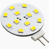
What is Bennic Bypassing Capacitor?
Bennic is a well-known brand in the audio and electronics industry, particularly for its capacitors, which are often used in bypassing applications. A bypass capacitor is placed across a power supply to reduce noise and improve the stability of a circuit. It essentially filters out unwanted signals, ensuring that only the clean, desired frequencies pass through. Bennic capacitors have earned a reputation for reliability and quality in both audio and electronic applications.
However, when you ask, “What is better than a Bennic bypassing capacitor?” the answer depends largely on the specific application. Some other brands or types of capacitors may offer better performance depending on factors like capacitance values, temperature stability, or frequency response.
What Type of Capacitor is Best for Bypass?
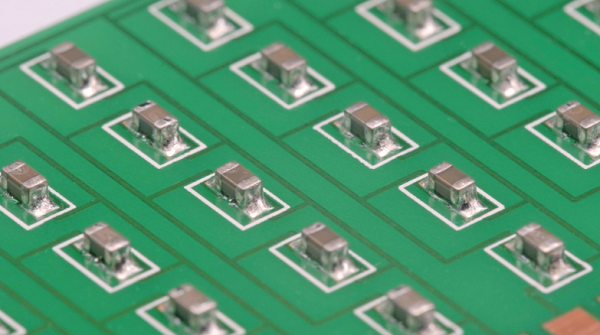
The type of capacitor most suitable for bypass is the multilayer ceramic capacitor (MLCC).
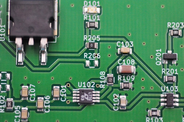
Multilayer ceramic capacitors (MLCCs) are the first choice for bypass capacitors due to their small size, low equivalent series resistance (ESR), low equivalent series inductance (ESL) and wide operating temperature range. These characteristics enable MLCC to effectively suppress high-frequency noise signals and interference signals to ensure circuit stability and signal quality. Although MLCC has some drawbacks, such as capacitance values that may vary dynamically with temperature, DC bias, and AC signal voltage, and the piezoelectric properties of dielectric materials that may convert vibration or mechanical shock into AC noise voltage, the impact of these drawbacks is acceptable in most applications. Due to its small footprint and low cost, MLCC is used in almost every electronic device, although more careful evaluation may be required in noise-sensitive applications.
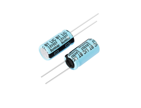
Compared to MLCC, solid tantalum electrolytic capacitors are less sensitive to the effects of temperature, bias, and vibration, which makes them potentially a better choice in specific situations. However, the wide application of MLCC and its excellent bypass performance make it the first choice for bypass capacitors.
What is Better Than Bennic Bypassing Capacitor?
While Bennic capacitors are highly regarded, other high-quality brands and capacitor types might perform better depending on the context of use. For high-end audio applications, Mundorf capacitors are often praised for their superior sound clarity. Nichicon capacitors are another top-tier choice, known for their exceptional performance in both audio and power applications.
If you’re looking for capacitors with higher temperature stability, capacitors from Wima or Vishay could be a better choice. They are known for their high precision and reliability in high-temperature environments. Additionally, some film capacitors, like those from the Mundorf EVO series, might surpass Bennic capacitors when it comes to audio fidelity.
What Size Bypass Connection Do I Need?
The size of the bypass capacitor you need depends on the circuit’s power requirements and frequency range. For power supplies in typical electronic circuits, bypass capacitors range from 0.01 µF to 100 µF, depending on the specific requirements. For audio applications, where Bennic capacitors are frequently used, you may see values from 1 µF to 10 µF.
In power circuits, you might want to use larger capacitors, like 10 µF or higher, to smooth out lower-frequency noise. For higher-frequency noise, smaller capacitors, like 0.1 µF, tend to work better. It’s also important to choose a capacitor with a voltage rating that exceeds the operating voltage of the circuit to ensure reliability.
What Type of Bypass Capacitor Works Best at High Frequency?
At higher frequencies, ceramic capacitors are often the best choice for bypassing. Their low equivalent series resistance (ESR) and inductance make them ideal for filtering out high-frequency noise. Multilayer ceramic capacitors (MLCCs) are particularly effective in such cases because they can provide excellent high-frequency performance while maintaining small physical sizes.
Electrolytic capacitors, on the other hand, may not perform as well at higher frequencies due to their higher ESR and inductance. For ultra-high-frequency applications, you might also consider using tantalum capacitors or specialized film capacitors.
How to Choose the Value of a Bypass Capacitor?
Choosing the right value for a bypass capacitor is crucial to the performance of any electronic circuit, particularly those dealing with noise-sensitive components like op amps, microcontrollers, and RF circuits. The value of the capacitor determines its effectiveness at filtering out unwanted noise across different frequencies. Here are the key factors to consider:
Target Frequency
The first step is to determine the frequency range of the noise you want to filter out. For lower-frequency noise, you’ll need a larger capacitance value. Capacitors in the range of 10 µF to 100 µF are typically used to filter low-frequency noise, such as power supply hum. For higher-frequency noise, a smaller capacitor, such as 0.01 µF to 0.1 µF, is often more effective. In many cases, circuits will use multiple capacitors to address different frequency ranges (a practice known as multi-capacitor bypassing).
Capacitor Type
Different types of capacitors have different characteristics that can affect the bypassing performance. Ceramic capacitors are often preferred for high-frequency noise filtering because of their low equivalent series resistance (ESR) and inductance. Electrolytic capacitors, while having higher capacitance, tend to have higher ESR.
Operating Voltage
It’s crucial to select a capacitor with a voltage rating that is at least 20-50% higher than the circuit’s operating voltage. For instance, in a 5V circuit, a capacitor rated for 10V or higher would provide a safe margin of operation.
Temperature and Environmental Considerations
If your circuit operates in environments with extreme temperatures, make sure to choose capacitors that are rated for those conditions. Ceramic capacitors with a C0G (or NP0) dielectric offer excellent temperature stability. On the other hand, capacitors with X7R or Y5V dielectrics are more susceptible to capacitance changes over temperature, so they may not be the best choice for precise applications.
Application-Specific Requirements
In audio circuits, where noise can severely affect sound quality, precision and high-quality capacitors are often used. Meanwhile, in power circuits, a combination of electrolytic and ceramic capacitors might offer the best balance between high and low-frequency filtering.
What is the Difference Between a Decoupling Capacitor and a Bypass Capacitor?
Though decoupling and bypass capacitors serve similar functions, they are used slightly differently. A bypass capacitor is specifically designed to filter out noise from the power supply, allowing only the desired signals to pass through.
A decoupling capacitor, on the other hand, helps to isolate different parts of a circuit, ensuring that changes in current from one part don’t affect other parts. It works as a buffer, absorbing noise and voltage fluctuations that could otherwise cause instability in the circuit.
In many cases, the terms are used interchangeably because bypass and decoupling capacitors often serve both purposes in a circuit.
Does Bypass Capacitor Increase Gain?
A bypass capacitor does not directly increase gain, but it does help improve the overall performance of an amplifier. In some amplifier circuits, bypass capacitors help reduce noise and stabilize the power supply, which can indirectly contribute to better signal quality and perhaps an apparent increase in gain.
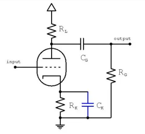
For instance, in common-emitter amplifier circuits, a bypass capacitor across the emitter resistor can increase the gain by reducing the feedback signal. By filtering out unwanted signals, the circuit can focus on amplifying the desired signal more effectively.
Why Use Multiple Bypass Capacitors?
Using multiple bypass capacitors of different values is a common practice to cover a wide range of frequencies. Different capacitors excel at filtering different frequencies. A larger capacitor (e.g., 10 µF) is typically used to filter out low-frequency noise, such as power supply ripple, but its effectiveness diminishes at higher frequencies due to parasitic inductance. On the other hand, smaller capacitors (e.g., 0.1 µF or 0.01 µF) are more effective at higher frequencies but may not be able to handle lower-frequency noise. In addition to this, here are some other benefits we can get when using multiple bypass capacitors:
- Broad frequency coverage
- Low ESR and inductance
- Improved power supply stability
- Closer placement to noise sources
- Redundancy for reliability
What Happens to the Output Voltage if Bypass Capacitor is Removed?
If a bypass capacitor is removed from a circuit, you may notice increased noise and instability in the output voltage. The capacitor helps to filter out high-frequency noise and smooth out fluctuations in the power supply. Without it, the circuit becomes more susceptible to unwanted interference, which could result in a noisy or distorted signal.
In some cases, removing a bypass capacitor can also affect the circuit’s gain, particularly in amplifiers, where the capacitor helps to control signal feedback.
Do Op Amps Need Bypass Capacitors?
Yes, operational amplifiers (op amps) typically require bypass capacitors to ensure stable operation. Op amps are highly sensitive to power supply fluctuations. Without proper bypassing, noise from the power supply can couple into the op amp’s signal path, causing distortion, oscillation, or instability. Op amps with high gain are particularly prone to oscillation if there’s noise in the power supply. A bypass capacitor across the op amp’s power pins can prevent oscillations by stabilizing the voltage supply.
EBest Circuit (Best Technology) provides one-stop service for our customers, not only for PCB and PCBA assembly, but also components sourcing. If you have PCBA projects, but don’t want to buy components by yourself, welcome to contact sales@bestpcbs.com, we are happy to help you!