Circuit board white is more than just an aesthetic trend. It’s quickly becoming a common choice in PCB (Printed Circuit Board) design, thanks to its sleek look and unique benefits. When compared to traditional PCBs, white circuit boards offer enhanced performance and a polished finish that suits many modern applications. In this article, we’ll explore what makes circuit board white stand out, the advantages it offers, and why it’s gaining popularity in various industries.
What Is Circuit Board White?
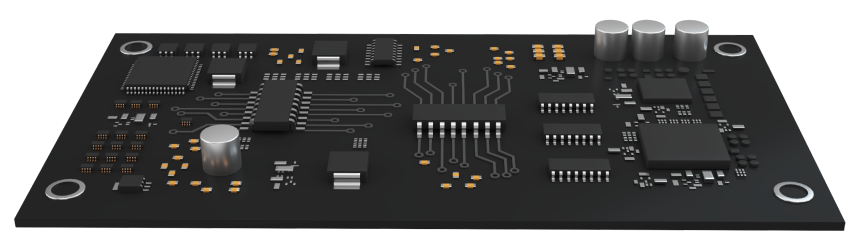
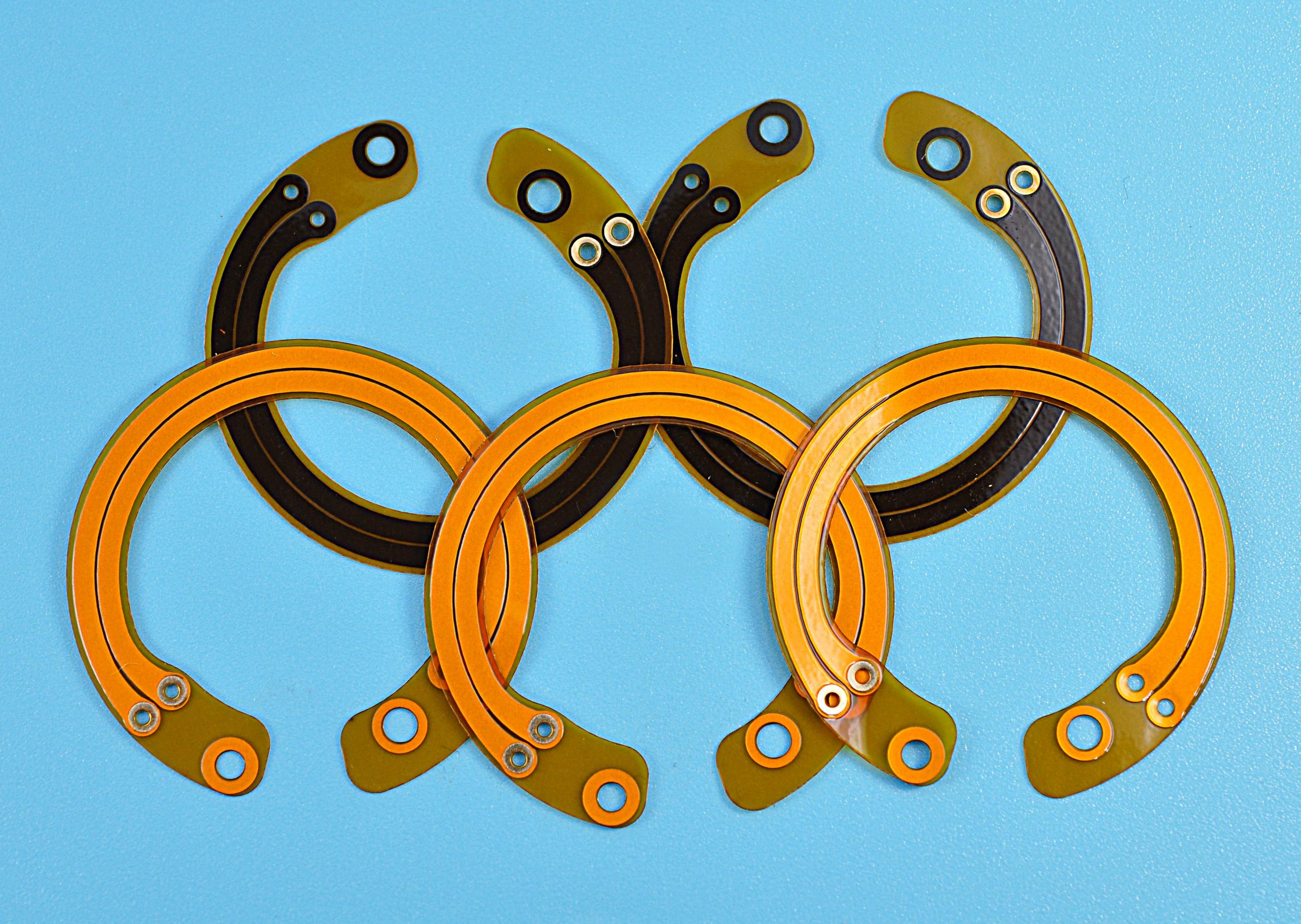
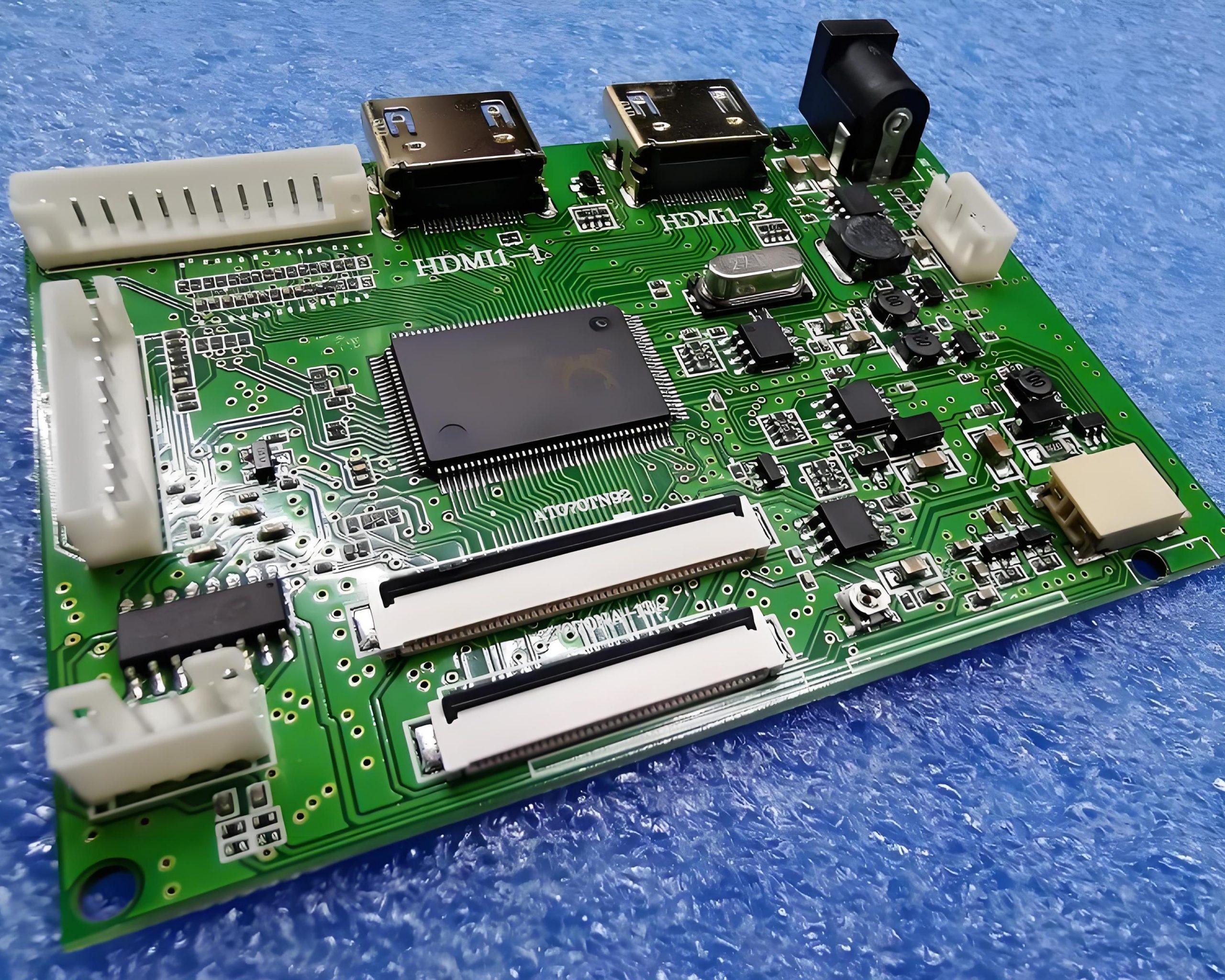
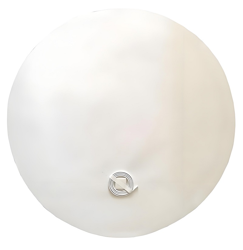
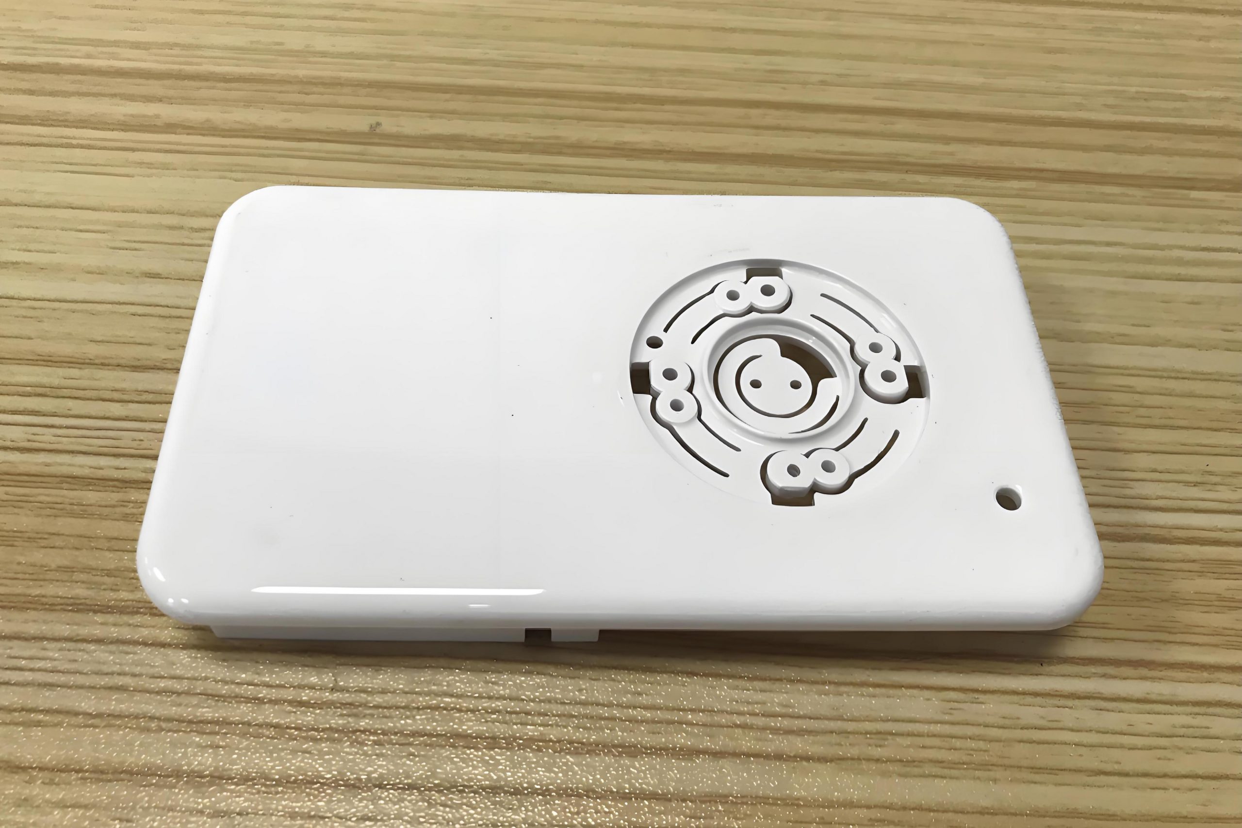
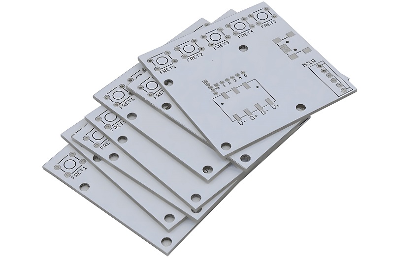
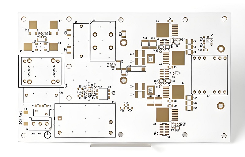
Circuit board white refers to PCBs that are produced with a white surface finish, rather than the typical green, black, or other colored finishes seen in standard PCBs. This white finish is achieved using specific materials and coatings that provide an eye-catching, clean look while still maintaining the reliability and performance that is expected from PCBs.
The choice of white as a color for PCBs may initially seem purely aesthetic, but it serves several functional purposes as well. It enhances the visual appeal of the circuit board, making it suitable for applications where appearance matters. But more importantly, the white surface helps in better heat dissipation, which is a critical factor in PCB design for high-performance electronics.
White PCB vs. Standard PCBs: What’s the Difference?
When comparing white PCBs to standard ones, the most obvious difference is the color, but there’s more to it than that. White PCBs are often constructed using materials that offer better heat management, which can improve the overall performance and lifespan of the device. Additionally, the reflective surface of a white PCB can provide better visibility for inspections, making the production process smoother.
On the other hand, traditional PCBs typically use green or black colors, which are cost-effective and effective in their own right. However, white PCBs may be preferred for high-end consumer electronics or products that require a more polished, professional appearance. They also often have a slight advantage in terms of thermal performance, as the white surface helps reflect heat away from the components.
In short, while traditional PCBs are still the go-to for most industries, white PCBs are emerging as the better option for those who need both form and function in their designs.
How White Printed Circuit Boards Improve Heat Dissipation?
Heat dissipation is one of the most critical factors in PCB design. Overheating can lead to performance issues and even failure of electronic devices. White printed circuit boards are known for their ability to dissipate heat more effectively than their darker counterparts. This is due to the reflective nature of the white surface.
The reflective properties help scatter heat away from the PCB, reducing the temperature buildup around sensitive components. This is especially useful in high-power applications like automotive systems, medical devices, and even some consumer electronics, where overheating could cause significant damage or degradation in performance.
By improving heat dissipation, white PCBs not only extend the life of the device but also enhance its reliability, making it a smart choice for demanding applications.
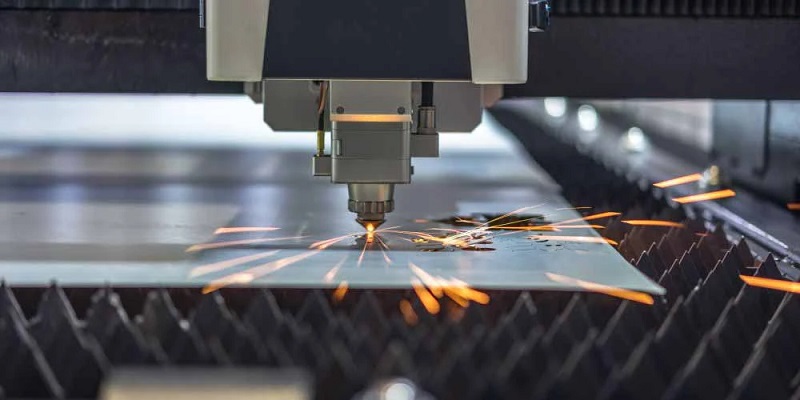
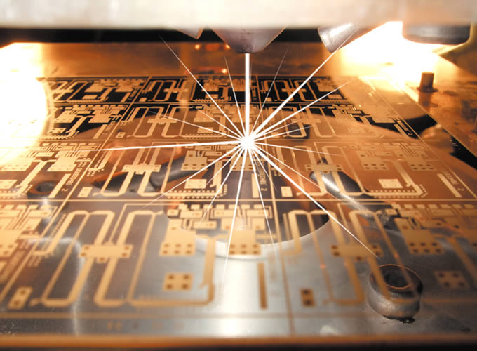
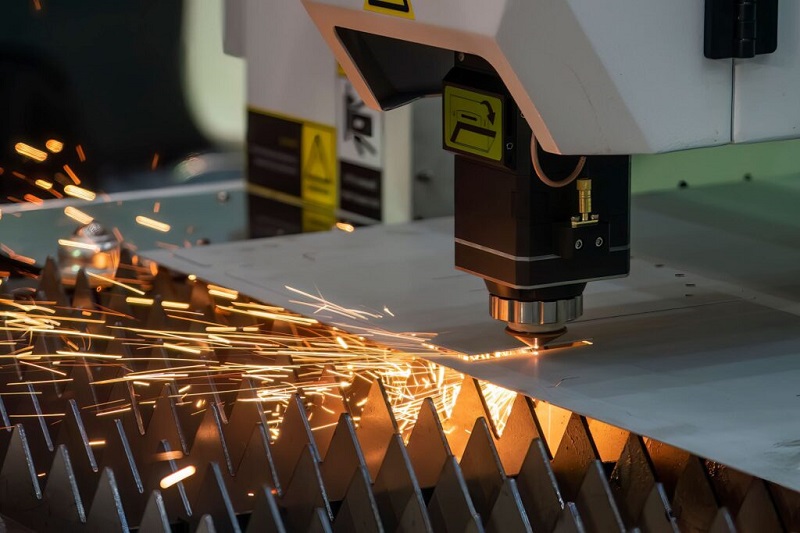
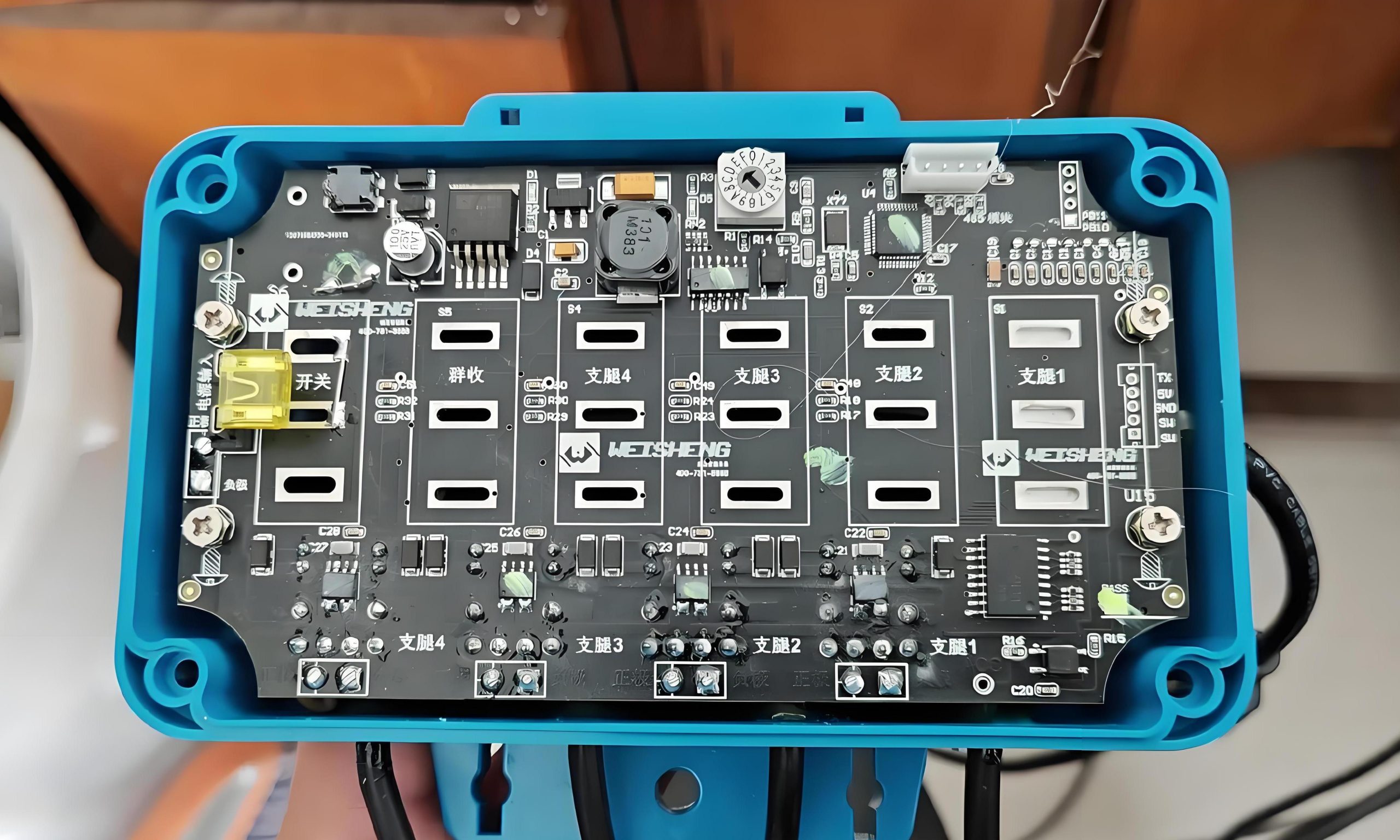
What Is the Manufacturing Process Behind White Printed Circuit Boards?
The manufacturing process for white printed circuit boards is similar to traditional PCBs, with a few key differences. First, manufacturers use specialized white coating materials that give the circuit board its bright appearance. These coatings are applied during the lamination process, where layers of copper, resin, and other materials are bonded together.
The process also involves precision etching to create the circuit pathways, just like in traditional PCBs. However, the final touch is the white coating, which is often baked onto the PCB to ensure it adheres properly and maintains its durability over time.
Due to the nature of the white finish, manufacturers have to pay extra attention to quality control during production. This ensures that the white surface remains smooth and uniform, contributing to both the aesthetic appeal and functionality of the PCB.
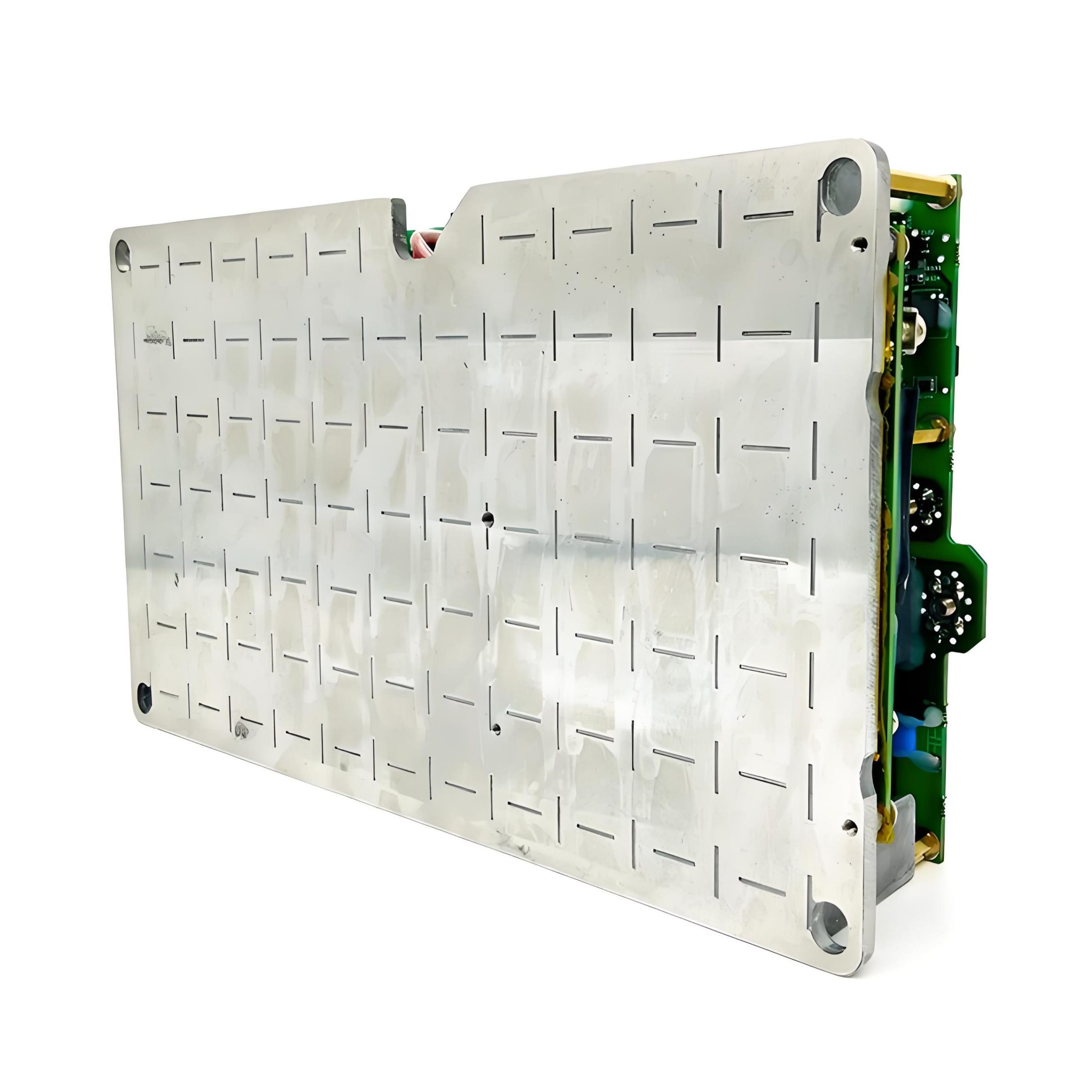
Are White PCBs More Durable Than Traditional Circuit Boards?
In general, the durability of a PCB depends on the materials used and the manufacturing process rather than the color. However, white PCBs tend to be slightly more durable when it comes to their surface integrity. The white coating used on these boards is typically designed to withstand harsh environments, making them resistant to scratches and other physical damage.
In addition to their surface resilience, the heat dissipation properties of white PCBs also contribute to their overall durability. By keeping the temperature within optimal levels, white PCBs help prevent the components from overheating, which could otherwise lead to premature wear and tear.
Overall, while the color itself doesn’t directly impact the PCB’s durability, the advanced materials and coatings used in white PCBs often offer a slight edge in terms of longevity and resistance to damage.
Which Top Industries Use White Circuit Boards in Their Products?
White circuit boards are increasingly finding their way into various industries due to their functional and aesthetic benefits. Some of the top sectors utilizing white PCBs include:
Consumer Electronics: White PCBs are commonly used in smartphones, wearables, and high-end home appliances due to their clean, modern look.
Medical Devices: In medical technology, where both aesthetics and performance matter, white PCBs help maintain device integrity while offering easy inspection.
Automotive Industry: White PCBs help manage heat dissipation in electric vehicles, which require reliable and efficient electronics.
Aerospace: The aerospace industry benefits from the lightweight and heat-reflective qualities of white PCBs, ensuring high performance under extreme conditions.
As demand for high-performance, visually appealing products grows, the use of white PCBs will continue to spread across these and other industries.
How to Customize White PCBs for Your Unique Needs?
One of the major advantages of white PCBs is the ability to customize them for specific requirements. Customization options include varying the thickness of the PCB, choosing materials that suit specific electronic needs, and even adjusting the white coating for different levels of reflectivity.
Customization also extends to the design of the circuit itself, where manufacturers can tailor the layout and connection paths to fit the unique needs of the application. Whether you’re working on a consumer product, medical device, or industrial equipment, customizing a white PCB can give your project a distinct edge.
By collaborating with a trusted supplier, you can ensure that your white PCBs meet both functional and aesthetic goals while staying within budget. EBest Circuit (Best Technology) is your trusted partner for high-quality, custom white PCBs, fast turnaround times, and excellent customer support. Get in touch with us at sales@bestpcbs.com for any questions or additional information.
Why Is Circuit Board White Gaining Popularity?
Circuit board white is gaining traction for several reasons. The most important factor is its balance of functionality and visual appeal. Consumers and designers alike are drawn to the sleek, modern appearance of white PCBs, which fit well with contemporary product designs.
Additionally, the thermal performance of white PCBs offers a significant advantage in a world where electronics are becoming more compact and powerful. As devices shrink in size but increase in power, efficient heat management becomes more critical.
Finally, the versatility of white PCBs means they can be used in a wide range of applications, from everyday gadgets to high-end technology. As industries continue to innovate, white circuit boards are expected to play a crucial role in advancing the capabilities and durability of modern electronics.
In conclusion, circuit board white is not just a passing trend but a technological innovation that offers both visual and functional benefits. From better heat dissipation to enhanced durability, white PCBs are well-suited for industries that demand both performance and aesthetics. With a focus on quality and speed, EBest Circuit (Best Technology) delivers customized PCBs alongside outstanding customer service. For inquiries or more info, just feel free to email us at sales@bestpcbs.com.