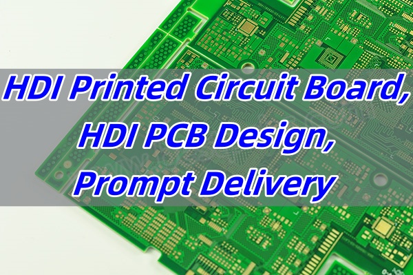
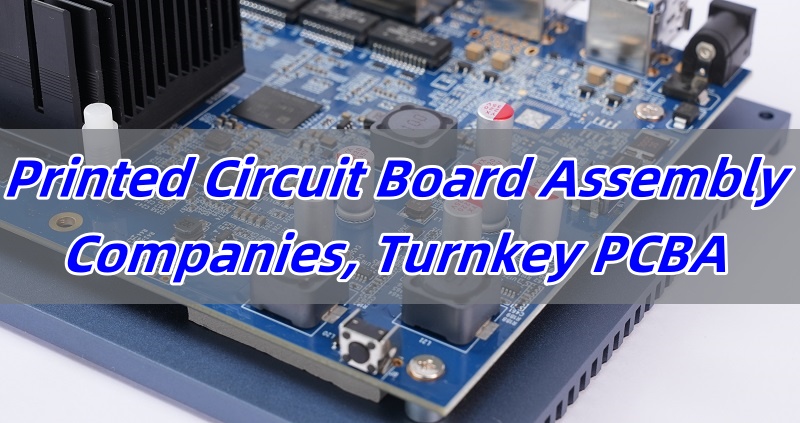
How 14 Layer PCB technology powers today’s most advanced electronics? This guide covers stack-up design, fabrication techniques, and how to choose the right manufacturer for high-density applications.
EBest Circuit (Best Technology) stands out as a premier 14 layer PCB manufacturer, offering fast-turn prototyping with industry-leading 24-72 hours delivery to accelerate your R&D cycle. Our advanced fabrication facilities support high-precision 14-layer stack-ups with strict impedance control (±5%), ensuring signal integrity for 5G, AI, and medical applications. With ISO 9001 & IATF 16949 certifications, we guarantee reliability from prototype to mass production. Clients benefit from DFM analysis upfront to avoid redesign costs, and 10+ years of HDI expertise for complex layouts. For urgent needs, our express engineering review cuts lead times by 30%. Contact sales@bestpcbs.com for a free stack-up design consultation and experience rapid iteration without quality compromise.
What Is 14 Layer PCB?
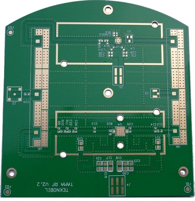
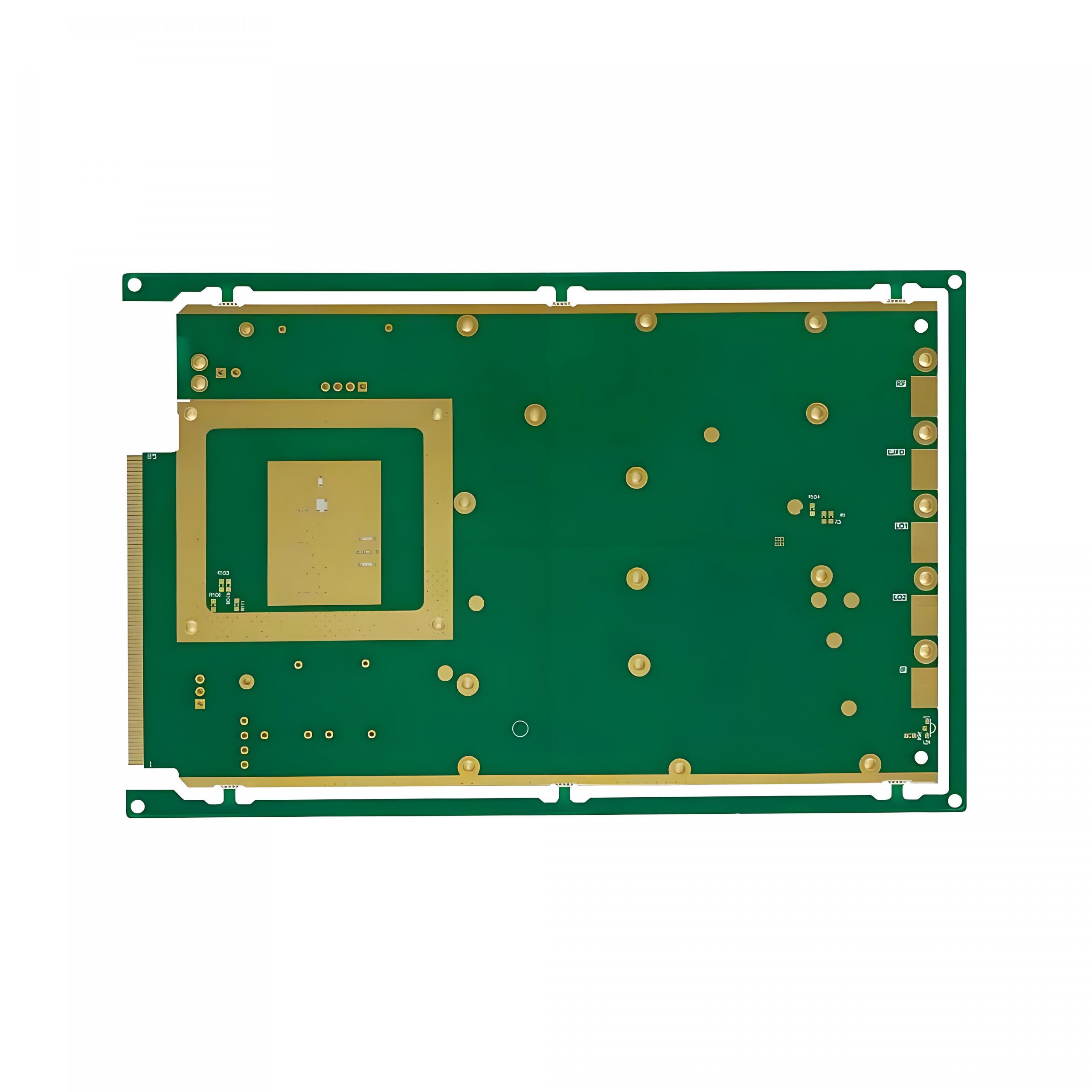
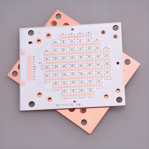
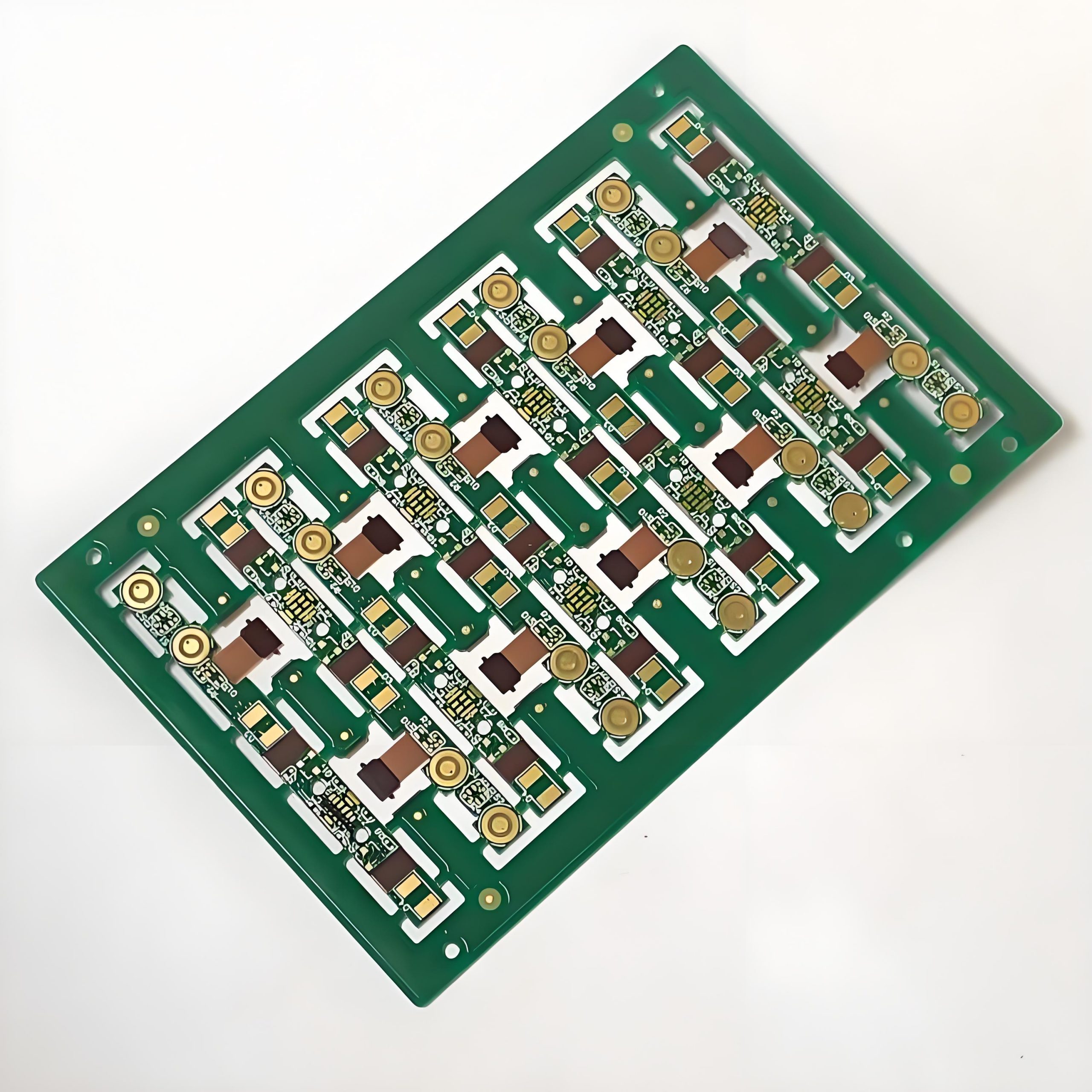
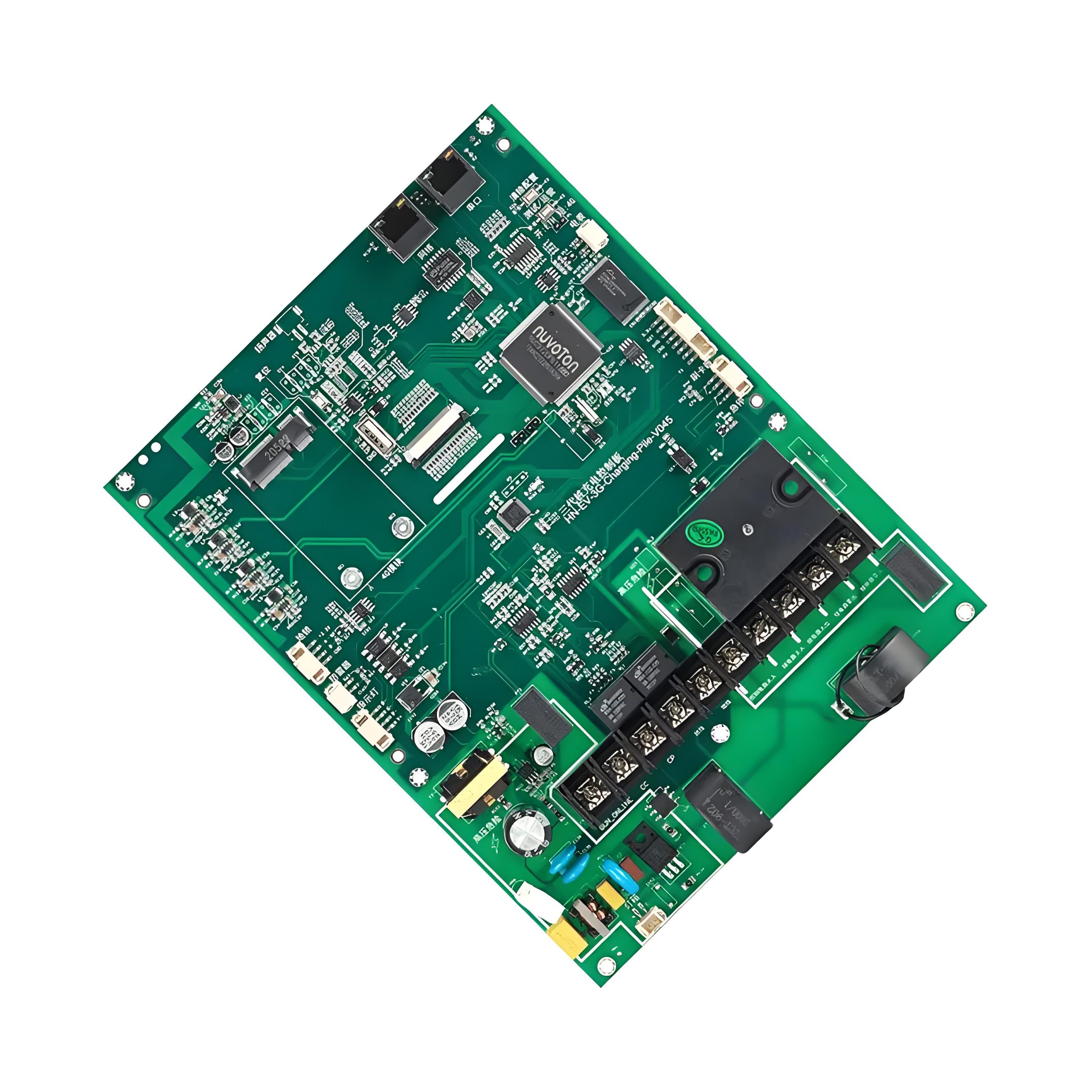
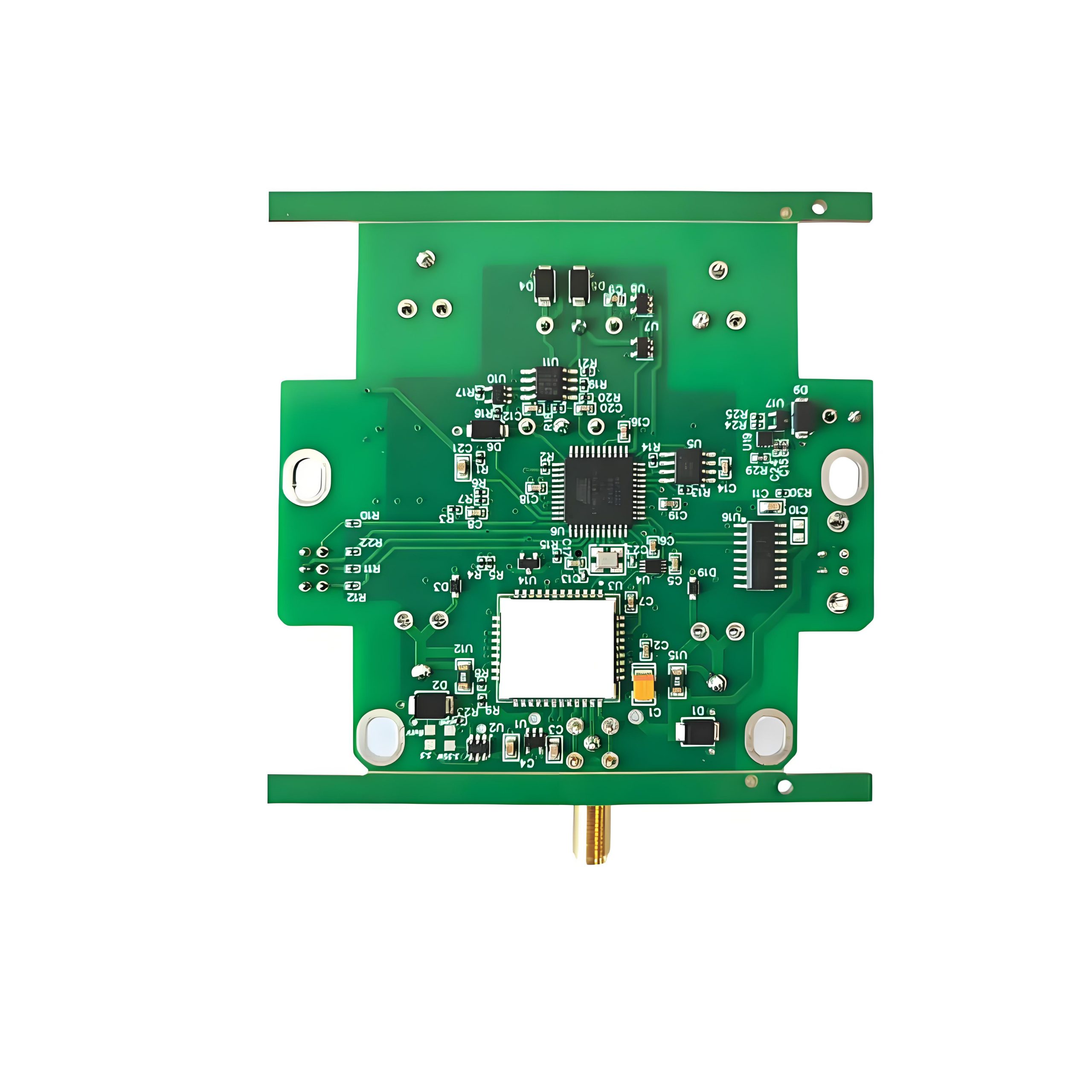
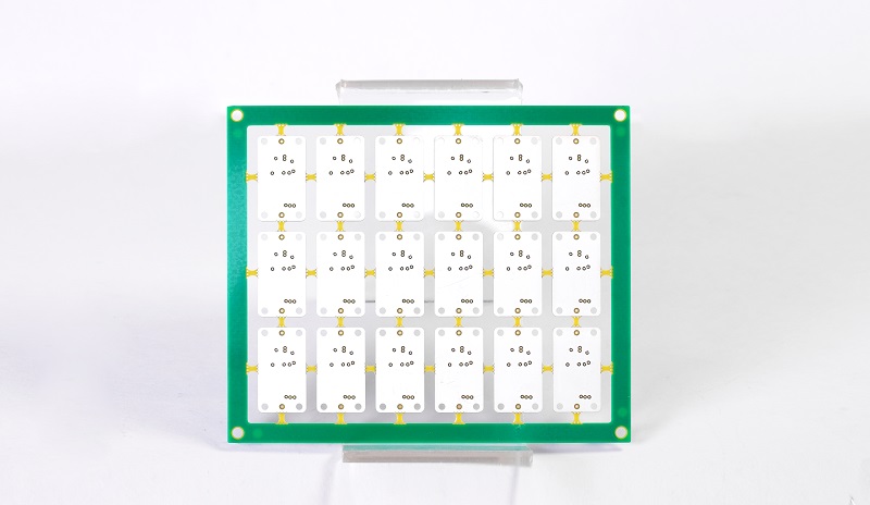
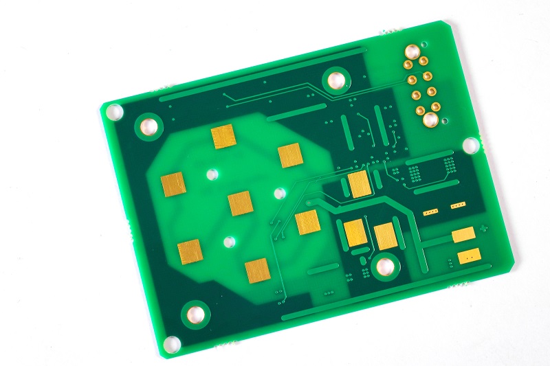
A 14 layer PCB is a printed circuit board that has 14 distinct layers of conductive material, typically copper, separated by insulating substrates. These layers work in harmony to create complex electrical pathways, enabling the efficient transfer of signals and power. With 14 layers, this type of PCB offers a significant amount of space for routing traces, integrating components, and managing power and ground planes. It’s commonly used in applications where high-density circuitry and advanced functionality are required. Whether it’s for high-speed data transmission systems or sophisticated electronic devices, a 14 layer PCB provides the flexibility and performance needed.

What Is Stack-up of 14 Layers PCB?
The layer arrangement of a 14-layer PCB directly influences its electrical performance, signal integrity, and manufacturability. Below is a structured breakdown of a typical configuration:
- Top Layer (Signal): This outermost layer handles high-speed signals, RF traces, or sensitive analog circuits. Its proximity to components makes it ideal for critical connections.
- Ground Plane: Positioned directly beneath the top layer, this plane minimizes electromagnetic interference (EMI) by providing a low-impedance return path for signals.
- Signal Layer 1: Dedicated to general-purpose signals, this layer balances routing density with impedance control requirements.
- Power Plane 1: Distributes power to multiple sections of the board, reducing voltage drops and ensuring stable operation.
- Signal Layer 2: Often used for low-speed signals or differential pairs, this layer benefits from the shielding effect of adjacent planes.
- Ground Plane: Enhances signal isolation and reduces crosstalk between adjacent signal layers.
- Signal Layer 3: Ideal for routing memory interfaces or high-speed buses, this layer leverages the controlled impedance environment.
- Internal Power Plane 2: Specifically designed for high-current loads or multiple voltage domains, this plane prevents noise coupling between power domains.
- Signal Layer 4: Supports mixed-signal routing, combining analog and digital traces with proper isolation techniques.
- Ground Plane: Maintains a symmetrical structure to prevent board warpage during thermal cycling.
- Signal Layer 5: Routes secondary high-speed signals or clock lines, benefiting from the proximity to the bottom ground plane.
- Power Plane 3: Serves as a dedicated power layer for noise-sensitive components, such as ADCs or DACs.
- Signal Layer 6: Handles low-frequency control signals or test points, ensuring accessibility for debugging.
- Bottom Layer (Signal): Similar to the top layer, this outermost layer accommodates connectors, mounting holes, or additional high-speed traces.
What Is Thickness of 14 Layers PCB?
The thickness of a 14-layer PCB depends on material selection, application requirements, and manufacturing constraints. Below is a detailed breakdown:
- Standard Thickness Range: Most 14-layer PCBs fall between 1.6mm (63 mils) and 2.4mm (94 mils). This range balances mechanical robustness, signal integrity, and cost-effectiveness.
- Material Contributions: Copper Layers – Each copper layer adds approximately 0.035mm (1.4 mils) per ounce of finished weight; Dielectric Substrates – Core materials (e.g., FR-4) typically range from 0.1mm to 0.2mm in thickness, while prepregs vary based on resin content.
- High-Speed Applications: For designs requiring tight impedance control (e.g., 5G or server boards), thinner dielectric layers may reduce overall thickness to 1.2mm–1.6mm. This minimizes signal propagation delays.
- Thermal Management: Boards with high-power components often incorporate thicker cores or metal substrates to enhance heat dissipation, increasing total thickness to 2.0mm–2.4mm.
- Mechanical Rigidity: Applications exposed to vibration or repeated flexing (e.g., automotive or aerospace) may use thicker boards (2.0mm+) to improve durability.
- Impedance Control: Thinner boards (e.g., 1.2mm) require precise layer stacking and dielectric selection to maintain consistent impedance across all 14 layers.
- Via Structures: Blind/buried vias or stacked micro-vias can reduce layer-to-layer spacing, allowing for thinner boards without sacrificing routing density.
- Assembly Tolerances: Thicker boards may require adjustments to solder paste stencil thickness or component placement accuracy during assembly.
- Cost Implications: Thinner boards often use specialized materials (e.g., low-loss laminates), which can increase costs compared to standard FR-4 builds.
- Customization: Non-standard thicknesses (e.g., 3.0mm+) are achievable but require careful coordination with manufacturers to ensure lamination consistency.

What Are Applications of 14 Layer PCB?
The complex architecture of 14-layer PCBs enables their use in demanding applications requiring high-speed performance, thermal resilience, and compact form factors. Below are application areas:
Advanced Communication Systems:
- 5G Base Stations: Handle mm Wave frequencies and massive MIMO configurations with controlled impedance routing.
- High-Speed Routers: Support multi-gigabit data rates across dense BGA packages and optical transceivers.
Industrial Automation:
- Programmable Logic Controllers (PLCs): Integrate real-time I/O processing with robust EMI shielding.
- Motor Drives: Manage high-current power stages while isolating sensitive control circuitry.
Medical Electronics:
- CT Scanners: Process high-resolution imaging data through synchronized multi-channel ADCs.
- MRI Machines: Maintain signal integrity in strong magnetic fields using low-loss dielectric materials.
Aerospace & Defense:
- Radar Systems: Achieve phase-coherent performance across distributed antenna arrays.
- Satellite Payloads: Withstand extreme temperature cycling with thermally conductive laminates.
Automotive Innovation:
- Autonomous Driving Modules: Process LiDAR, camera, and radar data in real-time with low-latency routing.
- Electric Vehicle (EV) Controllers: Balance high-voltage power distribution with isolated control logic.
High-Performance Computing:
- Servers & Data Centers: Enable multi-socket CPU configurations with DDR5 memory interfaces.
- AI Accelerators: Route high-speed SerDes links between GPUs and HBM stacks.
Consumer Electronics:
- Premium Smartphones: Support 5G mm Wave modules and multi-camera systems in slim form factors.
- Gaming Consoles: Deliver 4K/8K video processing with low-jitter clock distribution.
Renewable Energy Systems:
- Solar Inverters: Manage MPPT algorithms and grid synchronization under harsh environmental conditions.
- Battery Management Systems (BMS): Monitor cell voltages with precision analog front-ends.
How to Select A Reliable 14 Layer PCB Manufacturer?
Below are tips about how to select a reliable 14 Layer PCB manufacturer:
- Verify Advanced Equipment:
Ensure the manufacturer uses laser direct imaging (LDI) for precise trace definition and sequential lamination to handle 14-layer complexity without misregistration. - Confirm Material Expertise:
Check their experience with high-frequency laminates (e.g., Rogers 4350B) and specialized prepregs for tight impedance control in high-speed designs. - Review Quality Certifications:
Look for IPC-6012 Class 3 compliance and ISO 9001:2015 certification to ensure adherence to stringent quality standards. - Assess Impedance Control:
Confirm they offer time-domain reflectometry (TDR) testing to validate impedance tolerances (±5% or tighter) across all signal layers. - Evaluate Engineering Support:
Prioritize manufacturers who review your stack-up design, suggest via-in-pad or back-drilling optimizations, and resolve signal integrity issues pre-production. - Check Prototype Lead Times:
Choose partners with dedicated prototype slots delivering 14-layer boards in 5–7 business days using standardized materials and processes. - Inquire About First-Pass Yields:
Request data on first-pass yield rates for 14-layer boards—high yields (≥85%) indicate mature processes and robust quality controls. - Request Customer References:
Ask for case studies from clients in your industry (e.g., telecom, automotive) to gauge their experience with similar technical challenges.

Why Choose 14 Layer PCB Prototype for Your Design Validation?
Selecting a 14 Layer PCB Prototype for design validation provides actionable insights into real-world performance, enabling engineers to refine designs before full-scale production. Below are 10 specific measures to leverage during prototyping:
- Simulate Production Environments:
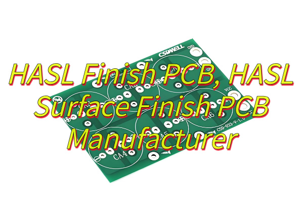
Use the 14 Layer PCB Prototype to replicate final manufacturing conditions, including material stacks, via structures, and surface finishes (e.g., HASL), ensuring accuracy in early-stage testing. - Validate High-Speed Signal Integrity:
Test PCIe Gen5, 100G Ethernet, or DDR5 interfaces on the prototype to identify reflections, crosstalk, or impedance discontinuities using TDR and bit-error-rate (BER) analysis. - Assess Power Delivery Networks (PDNs):
Measure voltage ripple, DC drop, and power integrity under simulated loads to optimize decoupling capacitor placement and layer-specific power plane designs. - Conduct Thermal Stress Testing:
Subject the 14 Layer PCB Prototype to extreme temperatures (-40°C to +125°C) while monitoring solder joint reliability and laminate stability with infrared cameras. - Evaluate Mechanical Durability:
Perform flex testing (e.g., 1,000+ bending cycles) to validate via resilience and board stiffness for automotive or portable device applications. - Verify Material Compatibility:
Confirm adhesion between HASL finish, solder mask, and component pads through cross-section analysis and IPC-TM-650 tape tests. - Map Impedance Continuity:
Generate layer-by-layer impedance profiles using TDR to ensure deviations stay within ±10% of target values (e.g., 50Ω for single-ended traces). - Inspect Via Quality:
Conduct microsectioning on plated-through holes (PTHs) to verify hole-wall copper thickness (≥1 mil) and annular ring integrity. - Optimize Panelization Strategies:
Use the prototype to test panel layouts, routing efficiency, and v-score/tab routing impacts on board yield and handling during assembly. - Gather DFM Feedback:
Collaborate with manufacturers to refine trace/space rules, stack-up symmetry, and copper balancing based on prototype findings.

How to Achieve 14 Layer PCB Prototype Fast Delivery?
To expedite the delivery of a 14 layer PCB prototype, implement these actionable strategies:
Optimize Design for Manufacturability (DFM):
- Use standardized trace/space rules (e.g., 3/3 mil) and avoid custom stack-ups to reduce engineering review time.
- Limit blind/buried vias to essential layers to simplify lamination cycles.
Leverage Rapid Prototype Services:
- Partner with manufacturers offering 24–48-hour design review turnarounds and 5–7 business day lead times for 14-layer boards.
Pre-Order Core Materials:
- Collaborate with suppliers to pre-stock frequently used laminates (e.g., FR-408HR, Megtron 6) to avoid material shortages.
Use Panelization Efficiency:
- Optimize panel layouts to maximize boards per panel (e.g., 4–6 units) while maintaining routing efficiency.
Adopt Automated Engineering Tools:
- Utilize CAM software for automatic DRC checks and impedance calculations to reduce manual setup time.
Prioritize Sequential Lamination:
- Choose manufacturers with in-house sequential lamination capabilities to avoid subcontracting delays.
Streamline Documentation:
- Submit complete fabrication packages (Gerber, NC drill, stack-up drawing) in a single file to minimize back-and-forth clarifications.
Expedite Impedance Testing:
- Request partial TDR testing on critical layers only (e.g., top 4 signal layers) to save 1–2 days in QA.
Use Courier Integration:
- Partner with logistics providers for same-day shipping post-production, leveraging air freight for urgent deliveries.
Plan for Contingencies:
- Allocate 10–15% budget buffer for rush fees and overnight shipping to avoid delays from unexpected issues.
How to Ensure Cost Control in 14 Layer PCB Mass Production?
To manage costs during 14 layer PCB mass production, implement these actionable strategies:
Standardize Material Selection:
- Use industry-standard laminates (e.g., FR-4, IS410) and avoid premium materials (e.g., Megtron 7) unless required for high-speed signals.
- Pre-negotiate bulk pricing for copper foils, prepregs, and solder masks with suppliers.
Optimize Layer Stack-Up:
- Balance copper distribution across layers to minimize lamination defects and reduce scrap rates.
- Avoid unnecessary blind/buried vias—use through-hole vias where possible to simplify drilling.
Automate Engineering Processes:
- Deploy CAM software for automatic DRC checks, impedance calculations, and panelization planning to reduce manual labor.
Implement Panelization Efficiency:
- Maximize boards per panel (e.g., 8–10 units) while maintaining 0.1″ routing channels to reduce per-unit material waste.
Streamline Testing Protocols:
- Skip full impedance testing on non-critical layers (e.g., power/ground planes) and focus on high-speed signal layers.
Negotiate Volume Discounts:
- Partner with manufacturers offering tiered pricing for orders ≥500 panels to secure 15–25% cost savings.
Reduce Setup Times:
- Use standardized drilling programs and tooling to minimize machine setup time between batches.
Adopt Lean Inventory:
- Implement JIT (Just-In-Time) material delivery to avoid overstocking and associated carrying costs.
Outsource Non-Core Processes:
- Partner with specialists for secondary operations (e.g., conformal coating, selective soldering) to reduce in-house labor.
Monitor Yield Metrics:
- Track first-pass yield rates and root-cause defective boards using Pareto analysis to eliminate recurring issues.
Conclusion
In summary, 14 layer PCBs represent a critical solution for high-density and high-performance electronic applications, requiring precise stack-up design, controlled thickness, and rigorous manufacturing standards. Their applications span aerospace, medical devices, and advanced computing systems, where reliability and signal integrity are paramount. Selecting a reliable manufacturer involves evaluating technical expertise, production capabilities, and quality certifications. Prototyping is essential for design validation, and partnering with a supplier offering fast delivery (e.g., 24-hour turnaround) ensures project timelines are met. For mass production, cost optimization strategies like panel utilization and material selection balance affordability and performance.