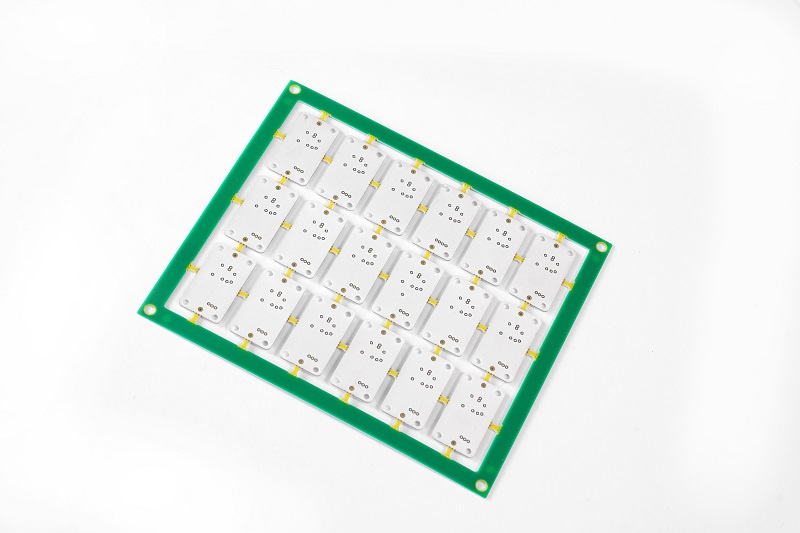
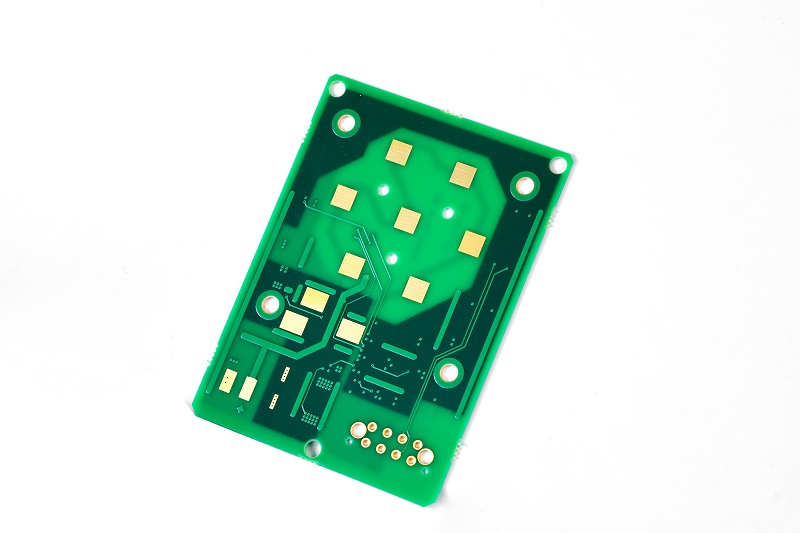
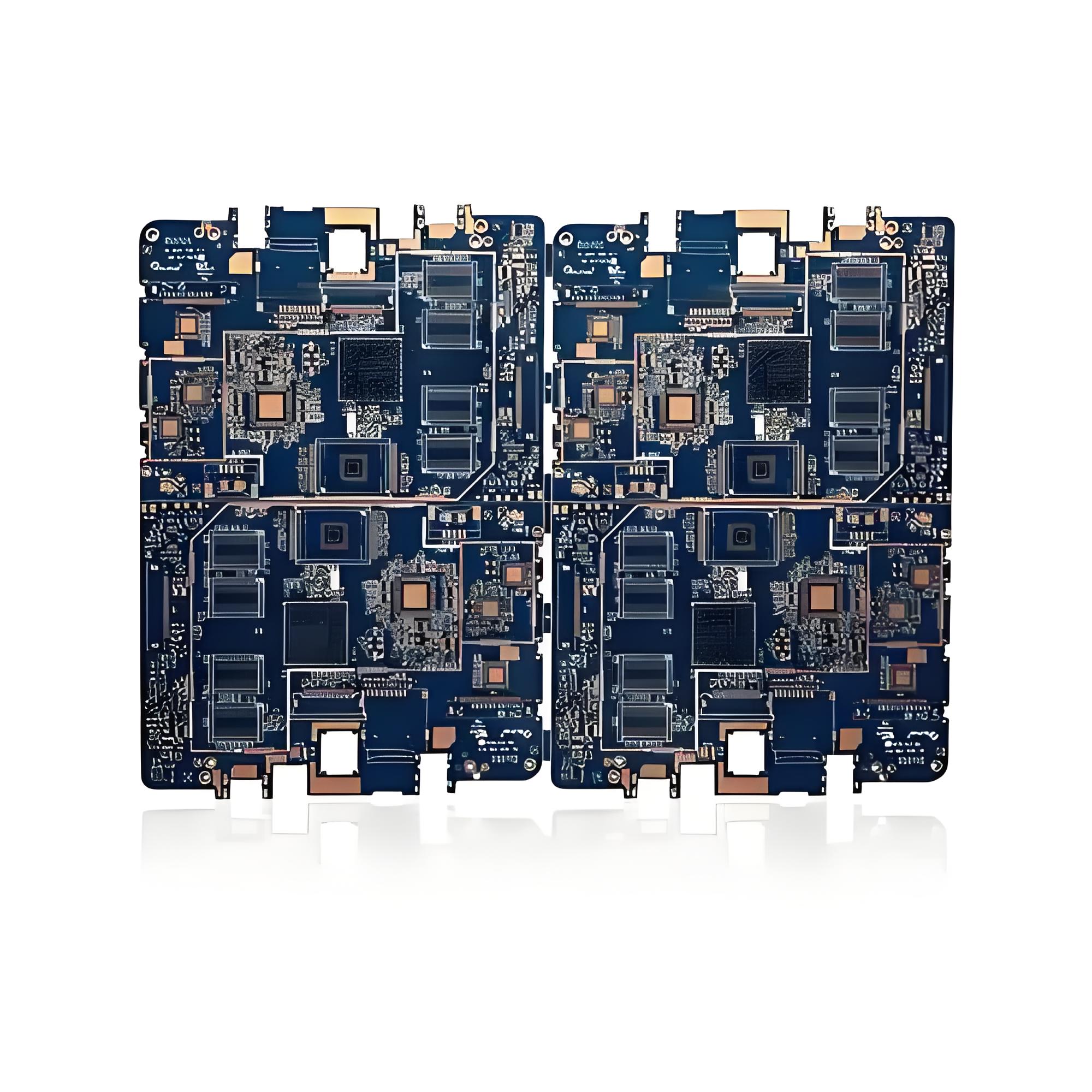
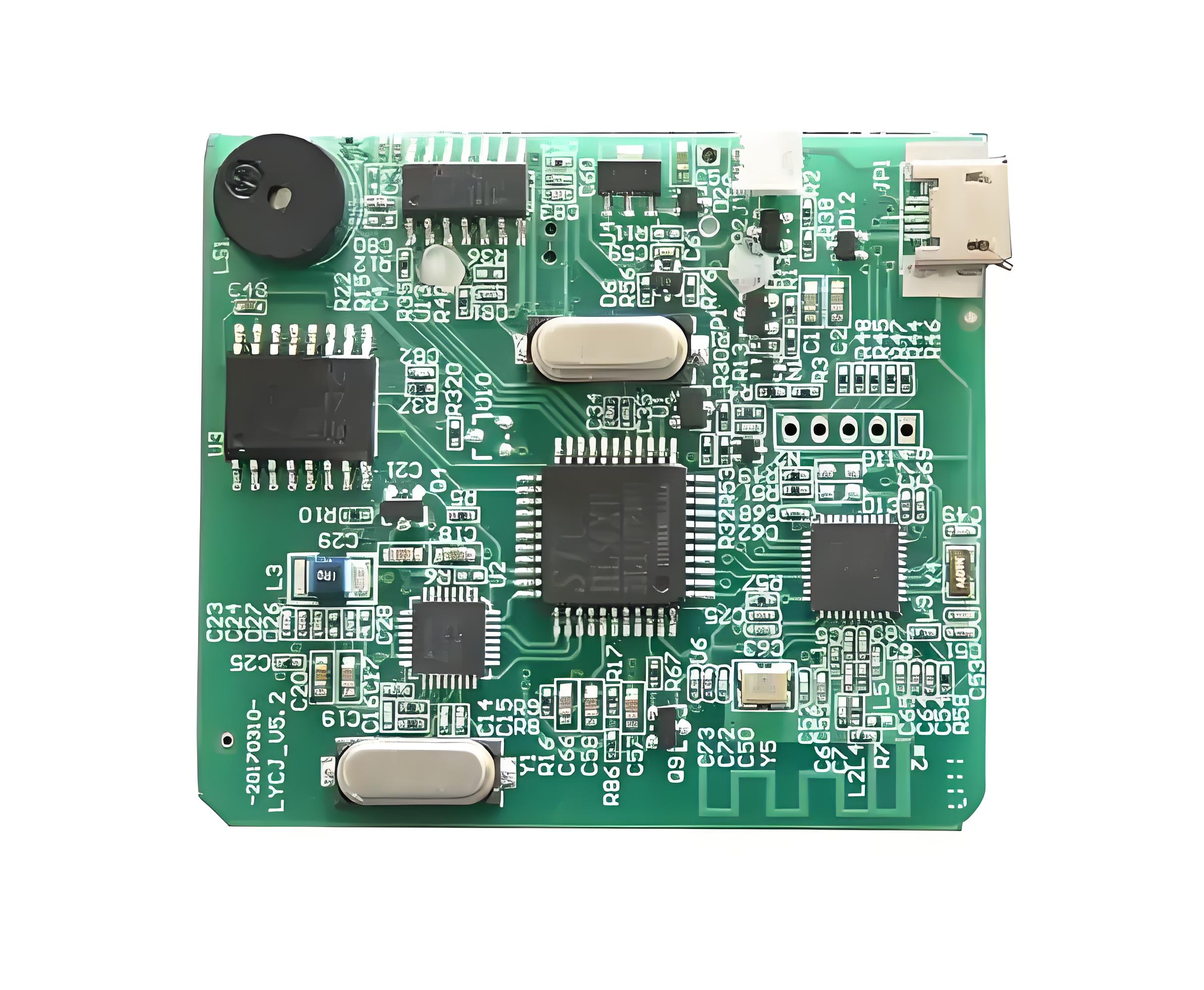
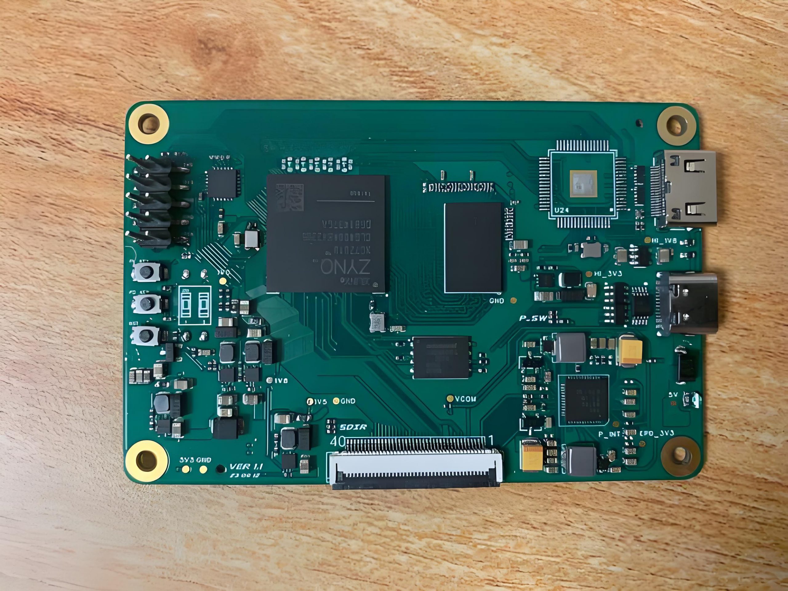
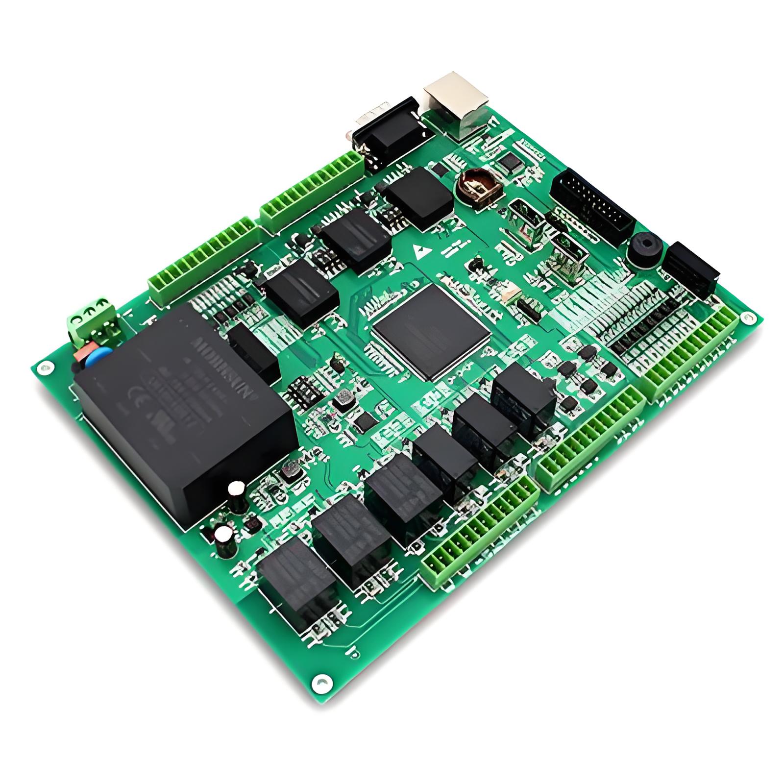
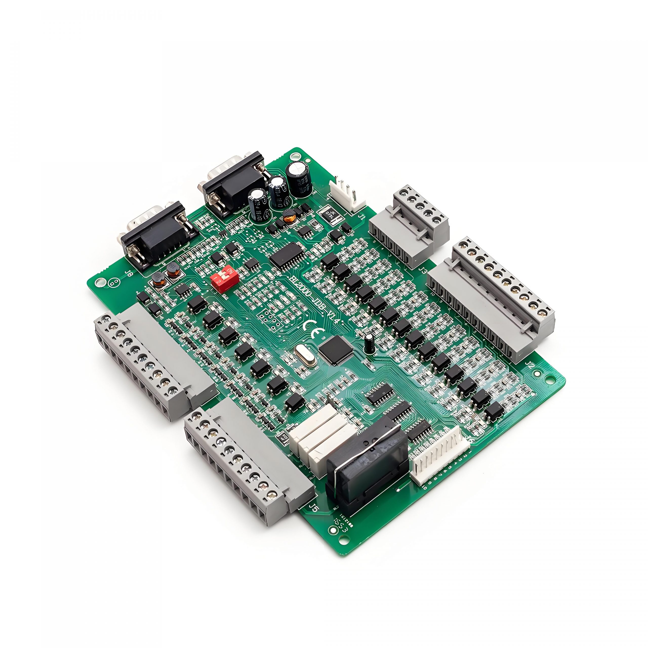
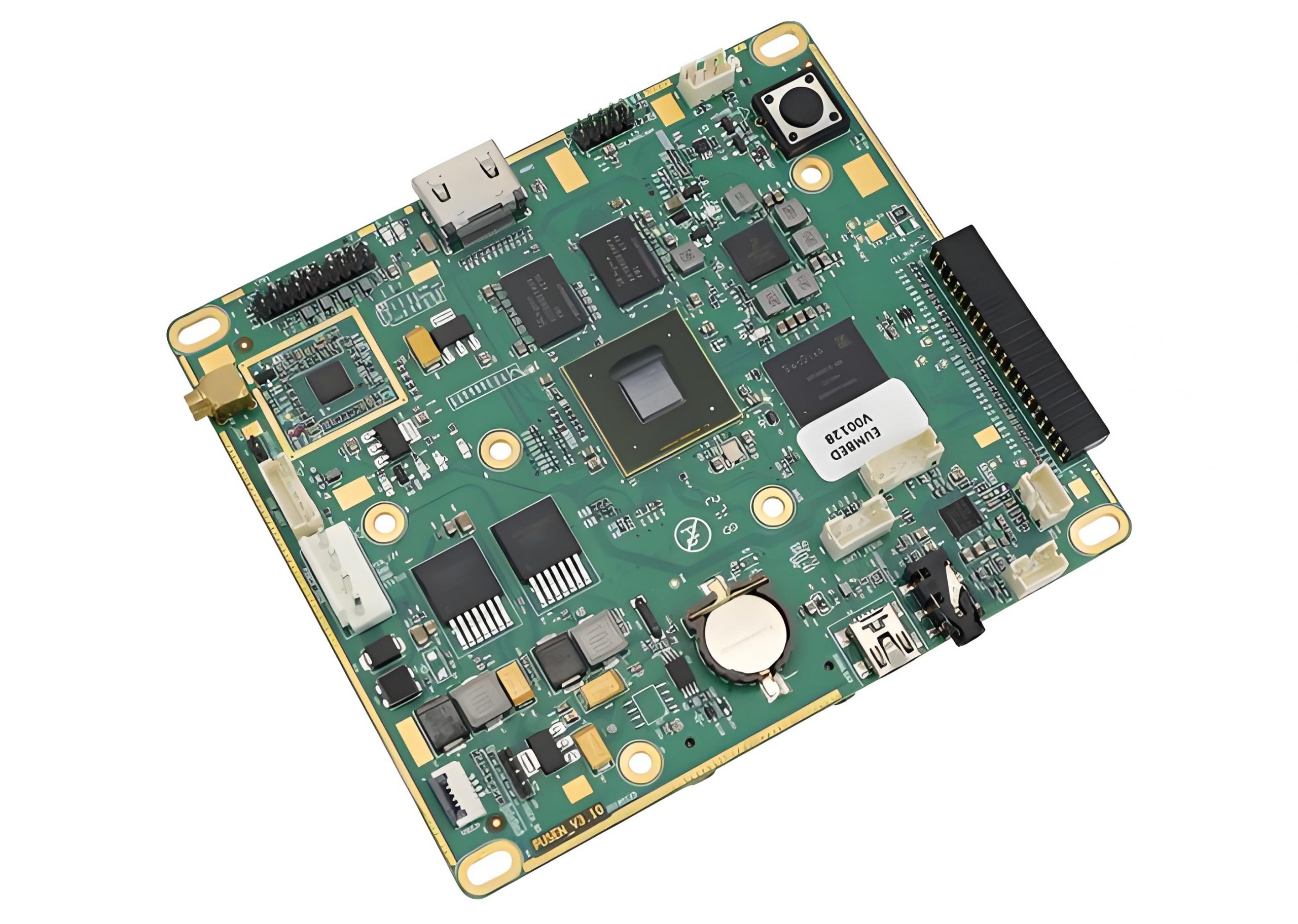
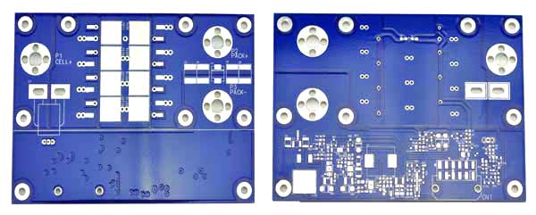
Custom circuit board design is the process of creating a PCB layout tailored to meet specific project needs. Unlike off-the-shelf solutions, a custom PCB gives you complete control over size, shape, layer stack-up, routing, and component placement. Whether you’re building a compact wearable, a robust industrial device, or a specialized automotive controller, a custom layout helps improve performance and space efficiency.
Who Needs a Custom Circuit Board Design?
Custom circuit boards are essential for engineers, startups, hardware developers, and OEMs who can’t rely on generic PCBs. If you’re designing a unique product or working with unusual form factors or power requirements, a custom design is your only option. This includes industries like:
- Medical devices needing miniaturized, high-reliability circuits.
- Automotive and aerospace systems requiring rugged, multilayer PCBs.
- Consumer electronics developers seeking sleek, compact designs.
- Industrial automation and control systems.
- Research and development teams creating prototypes.
In short, if your project demands specific functions, form factor, or performance that standard PCBs can’t deliver, it’s time for a custom solution.

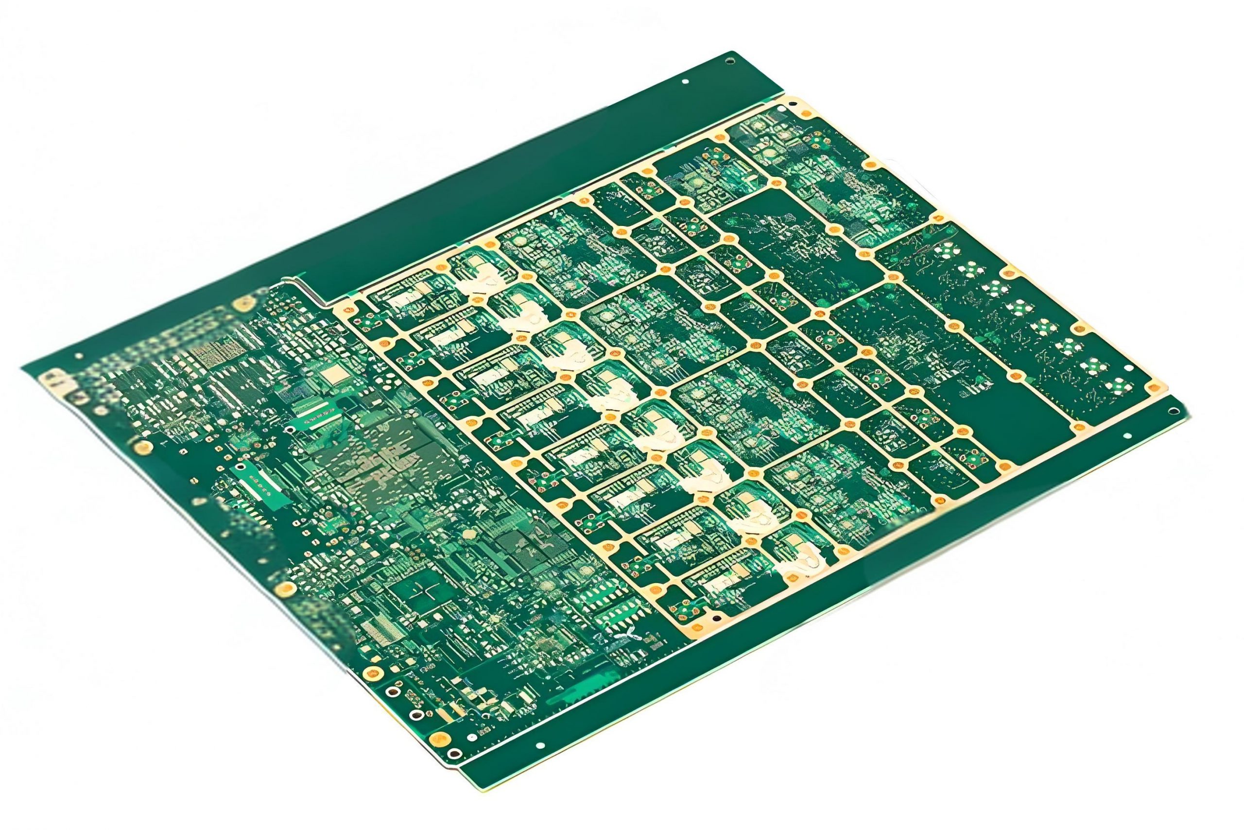
Circuit Board Design Rules
Design rules form the foundation of a reliable custom circuit board design. They’re not just about meeting DRC checks but ensuring your board works correctly in the field. Here are the most important and professional-level design constraints to follow:
1. Minimum trace width and spacing:
For standard 1 oz copper (35μm), a minimum trace width of 6 mil (0.15mm) is commonly used for signal lines. Power traces may require 10–20 mil or more, depending on the current. Use IPC-2221 charts or online calculators to determine width based on current (e.g., a 1A trace over 1oz copper typically needs 15 mil for internal layers, 10 mil for outer layers).
2. Minimum spacing:
Standard fabrication allows 6 mil spacing, but for HDI designs or high voltage isolation, use wider spacing. IPC-2221 recommends 63 mil (1.6mm) spacing for 250V isolation.
3. Via size and annular ring:
A typical via uses a 0.3 mm drill with 0.6 mm pad size, leaving a 0.15 mm annular ring. For HDI, microvias can be as small as 0.1 mm.
4. GND plane design:
Always use a solid ground plane on an internal layer. For multi-layer boards, dedicate one layer (often the second layer) as a continuous GND plane to reduce EMI and support return current paths. For analog and digital mixed-signal boards, separate analog GND and digital GND, and connect them at a single point near ADC/DAC.
5. High-speed signal rules:
Use controlled impedance for differential pairs and high-speed single-ended lines. Keep length mismatches for differential pairs within ±5 mils, and spacing between the pair should be 2–3 times the trace width.
6. Creepage and clearance:
Follow IPC-2221 standards for high-voltage boards. For instance, for 240V AC, you need minimum 3.2mm clearance between conductors.
7. DRC and design checks:
Always define your DRC settings based on your manufacturer’s capabilities. Most manufacturers support 4/4 mil (trace/space) in standard processes, but 6/6 mil is more commonly used for robustness.
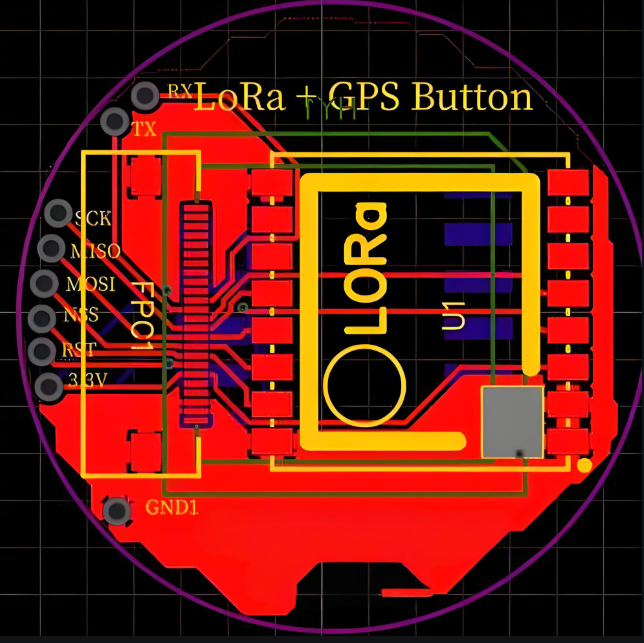
How to Layout Your DIY Circuit Board?
Laying out your custom PCB starts with strategy. A great schematic won’t save a poor layout, especially for fast signals or complex systems. Here’s a professional approach to DIY or low-volume layout:
1. Start with a block-level floorplan:
Divide your circuit into sections (power, MCU, analog, RF, connectors) and place them logically. Keep high-speed signals short and isolated from analog traces.
2. Place decoupling capacitors close:
Every IC power pin should have a 0.1μF ceramic capacitor placed within 1–2 mm of the pin, with a short path to the ground plane.
3. Use polygon pours for GND:
Instead of routing GND traces, pour solid copper polygons for GND connections. Ensure the polygon is tied to a proper ground net and has enough vias to connect to internal GND planes (1 via per 1–2 cm² area is a good rule).
4. Signal layer planning:
In a 4-layer board:
- Top layer: Signals and components
- 2nd layer: Solid GND plane
- 3rd layer: Power plane
- Bottom layer: Secondary signals
This gives you clean return paths and effective power distribution.
5. Controlled impedance routing:
For USB, HDMI, Ethernet, and RF signals, match the impedance (typically 50Ω single-ended or 100Ω differential). Use your PCB software’s impedance calculator or external tools like Saturn PCB Toolkit. Factors include trace width, dielectric height, and copper thickness. For instance, a 50Ω microstrip over 1.6mm FR-4 (εr=4.2) might require 12 mil trace width over 10 mil height.
- Differential pair routing:
- Keep equal length (match to within ±5 mils).
- Maintain consistent spacing.
- Avoid 90° bends—use two 45° bends or arcs.
6. Avoid stubs and isolated copper:
Any unused copper or hanging trace stubs can act as antennas. Remove them to reduce EMI.
7. Thermal relief and copper balance:
For through-hole pads connected to GND or power planes, use thermal reliefs to aid soldering. Also, ensure copper is balanced across layers to avoid warping.
PCB Design Software
You can’t design a custom board without the right software. Depending on your experience and budget, here are some options:
- KiCad (Free, open-source): Ideal for beginners and hobbyists. Offers schematic capture, PCB layout, and 3D visualization.
- EAGLE (Free for students and small projects): Good integration with Fusion 360 and supports complex designs.
- Altium Designer (Paid): Industry standard for advanced features like high-speed routing, simulation, and collaboration tools.
- EasyEDA (Cloud-based): Great for quick prototypes and integrates directly with fabrication services.
- OrCAD/PADS: Often used in professional environments for complex multilayer boards.
Choosing the right tool depends on your project’s needs, from simple prototypes to multilayer, production-ready boards. Here are the top 10 PCB design software that engineer commonly used.
Considerations During Designing a Custom Circuit Board
Designing a custom PCB isn’t just about making connections—it’s a balancing act between performance, cost, and manufacturability. Here’s what to consider:
- Board size and shape: Compact designs can save space but are harder to route.
- Number of layers: Multilayer boards improve performance but increase cost.
- Component availability: Choose parts that are easy to source and compatible with your assembler’s equipment.
- Thermal management: Use heat sinks, thermal vias, or copper pours to manage heat.
- Manufacturing capabilities: Make sure your design matches your fabricator’s limits for trace width, hole size, and stack-up.
- Testing and debugging: Leave space for test pads, headers, or diagnostic LEDs.
Thoughtful planning during the design phase saves time and avoids problems during production.
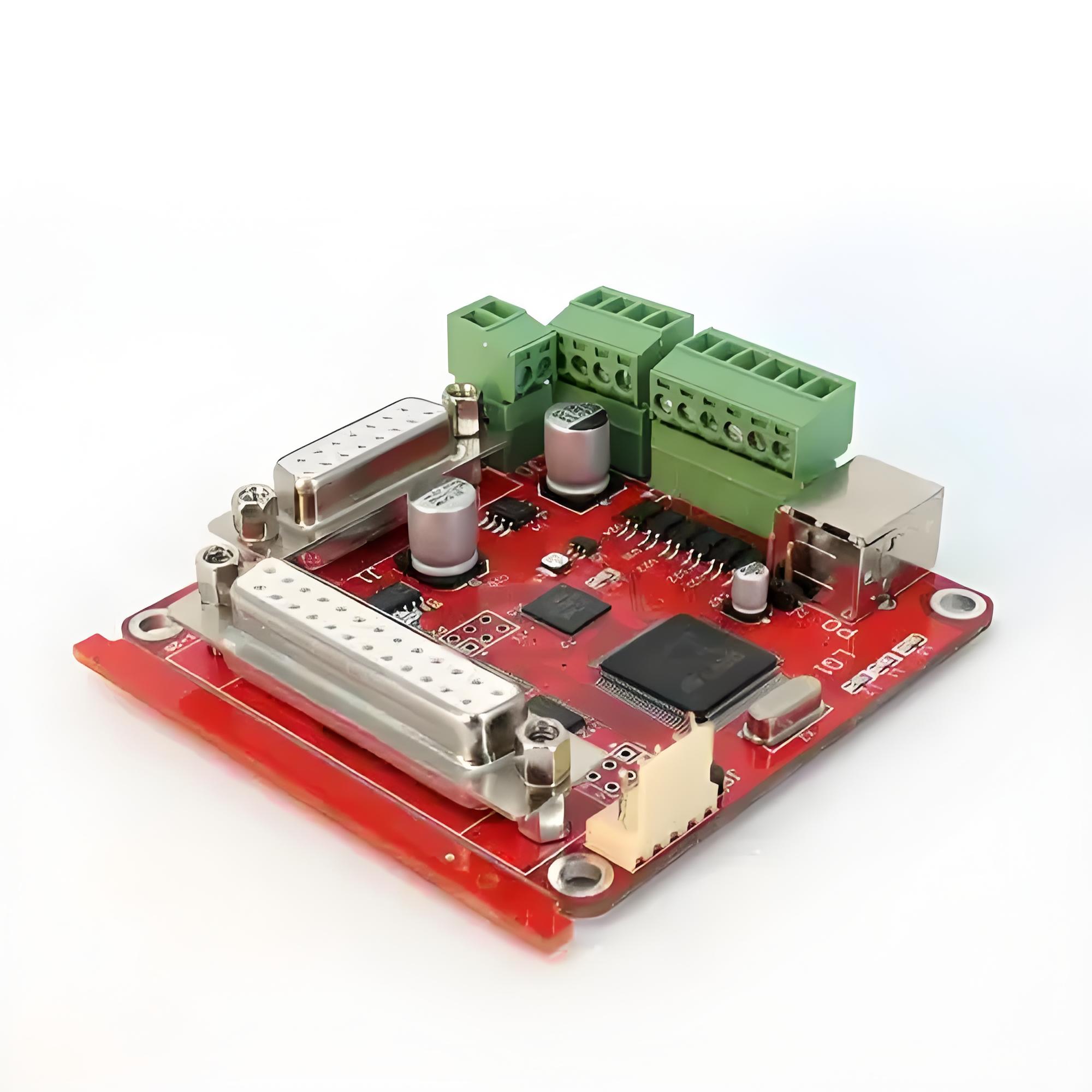
Where Can I Get a Custom Circuit Board?
You can order a custom circuit board from online PCB manufacturers or local fabrication shops. Some popular platforms include:
- JLCPCB
- PCBWay
- Sierra Circuits
However, if you’re looking for a highly reliable one-stop PCB solution with both fabrication and assembly services, it’s better to work with a professional company that understands the full production lifecycle.
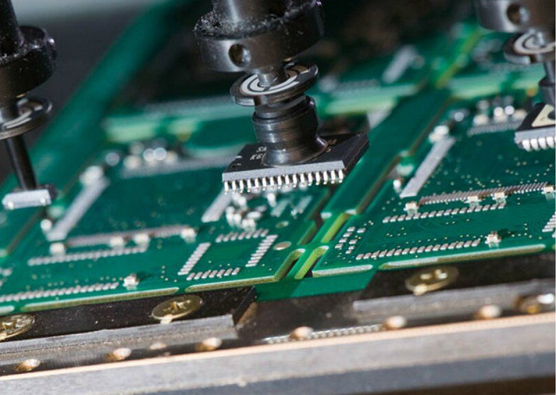
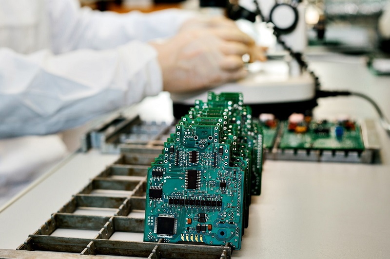
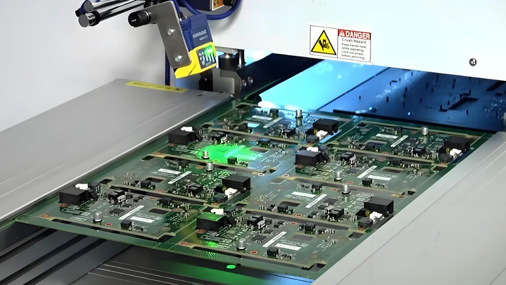
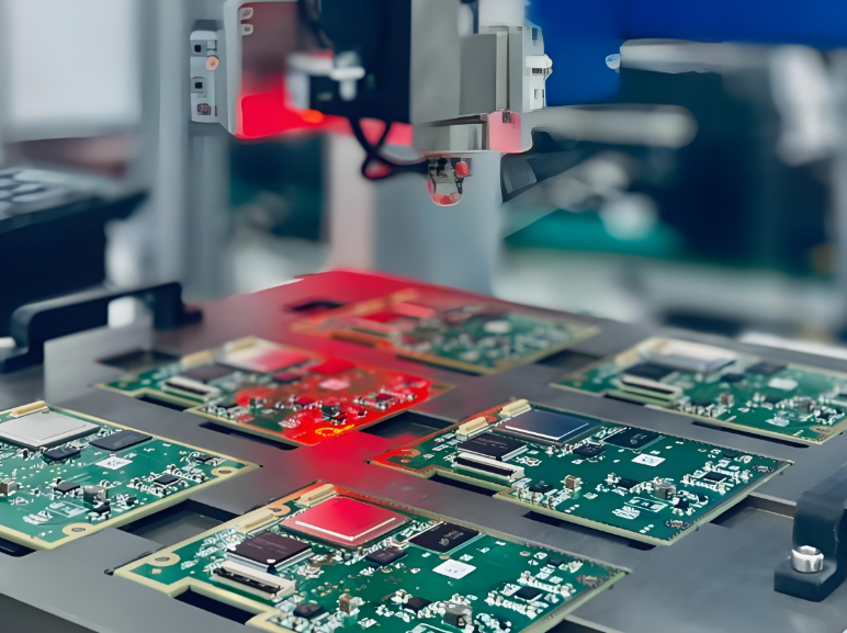
EBest Circuit (Best Technology) is your trusted partner for custom circuit board design, manufacturing, and assembly. With ISO9001, IATF16949, ISO13485, and AS9100D certifications, we follow strict quality systems to ensure that your project meets industry standards. Below are some advantages that customers why choose us:
- Full customization for single-sided, multilayer, ceramic, metal-core, and HDI boards.
- Advanced engineering support from schematic to layout optimization.
- Fast prototyping with 24/7 customer service and on-time delivery.
- Traceability with MES system, covering every process step for your peace of mind.
- Competitive pricing without compromising on quality.
Whether you’re a startup building a prototype or a Fortune 500 company scaling production, we’re here to support every step of your journey.
Contact us now to get a quote or free design consultation.
FAQs
1. What file format is needed to get a custom PCB made?
You’ll typically need Gerber files, CAD, BOM (Bill of Materials), and a pick-and-place file for assembly.
2. How long does custom PCB manufacturing take?
Depending on complexity and quantity, fabrication may take 3–7 days, with assembly adding 2–5 more days. Expedited service is available.
3. Can I get a custom PCB in small quantities?
Yes. Many manufacturers, including EBest Circuit (Best Technology), support low-volume and prototype runs.
4. Is custom PCB design expensive?
The cost depends on board complexity, number of layers, and turnaround time. Simple designs are very affordable today.
5. Do you help with PCB design revisions?
At EBest Circuit (Best Technology), yes—we offer design assistance and layout reviews to ensure your files are ready for production.