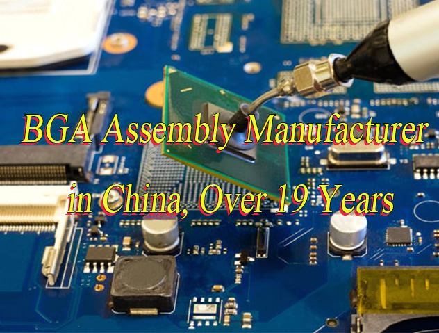
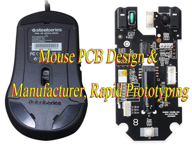
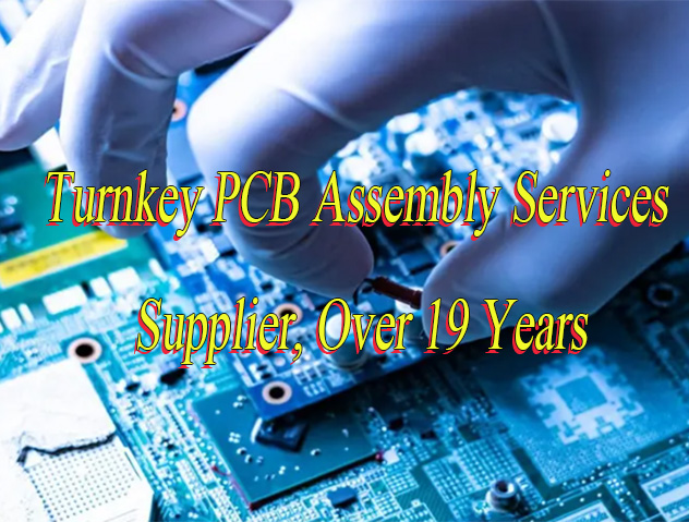
Why choose turnkey PCB assembly services? Let’s discover its definition, benefits, applications, assembly process and reliable supplier recommendation for turnkey PCB assembly services.
Are you worried about these questions?
- Struggling with design-to-production pitfalls? Component conflicts and pad defects causing yield collapse?
- Frustrated by high costs in small-batch trial production? Excessive per-board material and engineering costs, how to break through?
- Rushing for prototype validation but stuck with long lead times and miscommunication delays? How to accelerate progress?
As a turnkey PCB assembly services supplier, EBest Circuit (Best Technology) can provide you service and solutions:
- DFM Shield: Free Design for Manufacturing analysis to pre-empt 20+ process risks, boost yield by 20%+!
- Flexible Cost Reduction: Dedicated line for 10-500pcs batches, slashing per-board processing costs by 30%.
- 48-Hour Rapid Prototyping: From Gerber to sample in just 48 hours with dedicated support.
Welcome to contact us if you have any request for turnkey PCB assembly service: sales@bestpcbs.com.
What Is Turnkey PCB Assembly?
Turnkey PCB Assembly refers to a single supplier providing a complete service process, from design review and component procurement to PCB manufacturing, assembly, testing, and packaging. Customers only need to provide design files to receive a complete and usable finished circuit board. This model integrates supply chain resources, eliminating the complexity of coordinating multiple suppliers and achieving “plug-and-play” delivery.
Why Choose Turnkey PCB Assembly Services?
Advantages of Turnkey PCB Assembly Services:
- Full-Process Management: One-stop solution covering design, procurement, assembly, and testing, saves time and reduces coordination efforts.
- Cost Efficiency: Lowers costs by 15-30% through bulk purchasing, optimized processes, and reduced intermediaries, boosts profit margins.
- Quality Assurance: Strict IPC-A-610 standards with advanced inspection tools (AOI/X-ray), defect rates below 0.1%.
- Faster Time-to-Market: Cuts assembly time from 15-20 days to 7-10 days, supports 48-hour rapid prototyping for early market entry.
- Technical Expertise: Free DFM consultations and advanced engineering support (signal integrity, EMI/EMC), solves design challenges upfront.
- Scalable Production: Adapts from small batches to mass production, modular lines handle diverse PCB sizes/layers without capacity waste.
- Transparent Tracking: Real-time project visibility via online systems, automated alerts and remote audits ensure accountability.
When to Use Turnkey PCB Assembly Services?
Applications of Turnkey PCB Assembly Service:
- Rapid market feasibility verification for startups (48-hour rapid prototyping).
- Small- to medium-volume production of 50-50,000 units (adaptable to modular production lines).
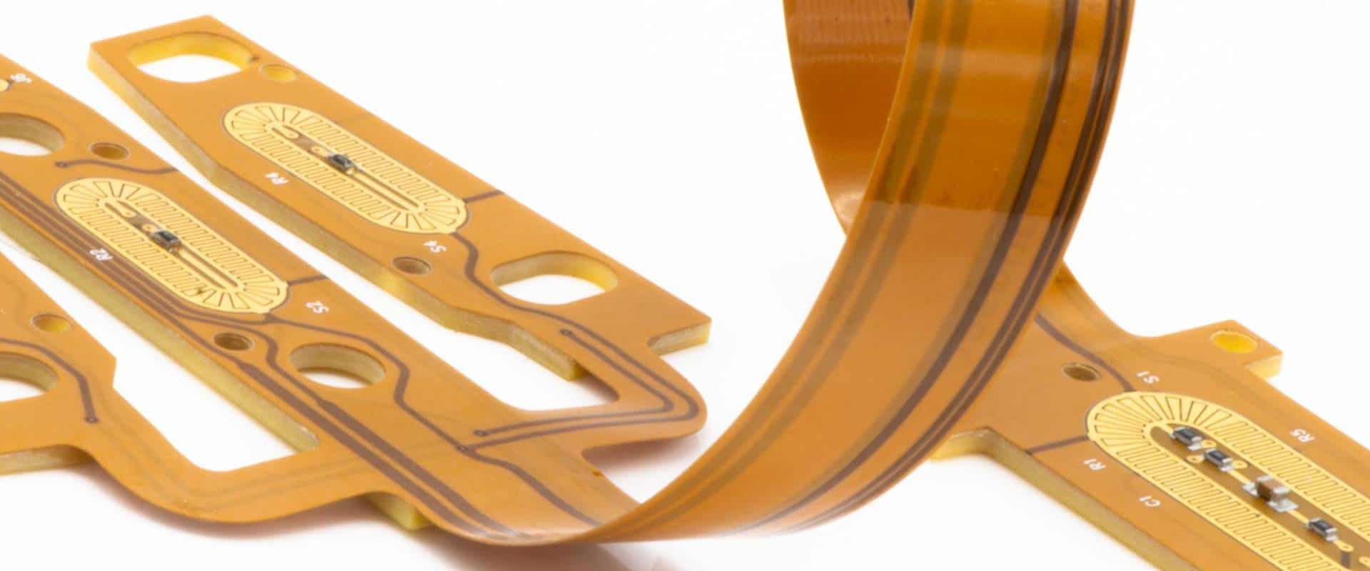
- High-frequency, high-speed, HDI, rigid-flex PCBs, and other complex process projects.
- Supply chain stability during periods of component shortages and price fluctuations.
- Quality control scenarios requiring ISO13485/IATF16949 certification for medical and automotive electronics.
What Problems Turnkey PCB Assembly Can Solve?
- Cost Efficiency Optimization: Turnkey PCB Assembly integrates design, procurement, manufacturing, and testing to reduce logistics, communication, and management costs. For example, bulk purchasing discounts and optimized inventory management cut single-board costs by 15–30% for overseas clients, especially small-batch production.
- Time Acceleration & Market Responsiveness: Single-supplier coordination shortens prototype cycles from 4–6 weeks to 2–3 weeks, enabling rapid design-to-test closure. This helps overseas clients seize market opportunities in time-sensitive sectors like consumer electronics and medical devices.
- Quality & Reliability Assurance: Expert teams control design specs, material selection, process parameters, and test standards, minimizing rework risks from design flaws or manufacturing errors. Techniques like AOI and X-ray inspection detect soldering defects early, ensuring compliance with standards (e.g., RoHS, UL) and boosting market trust.
- Supply Chain Simplification & Risk Mitigation: Overseas clients avoid cross-border supplier coordination, time zone gaps, and language barriers. Turnkey providers manage the full chain from component sourcing to final assembly, preventing delays from shortages or logistics issues and ensuring stable material supply via global networks.
- Flexible Production & Scalability: Supports elastic production from 10 prototypes to 10k+ volumes, eliminating frequent supplier changes. Startups can scale seamlessly from small-batch validation to mass production, reducing changeover costs and technical adaptation issues.
- Technical Support & Optimization: Offers design optimization (e.g., PCB layout, thermal management), material guidance, and process improvements. Simulation tools predict design flaws, and cost-effective component alternatives enhance performance while cutting costs for overseas clients.
- Risk Sharing & Compliance Guarantee: Providers assume liability for manufacturing defects and test failures, freeing clients from complex production issues. Familiarity with regulations (e.g., EU REACH, FCC) ensures compliance, reducing market entry barriers for overseas clients.
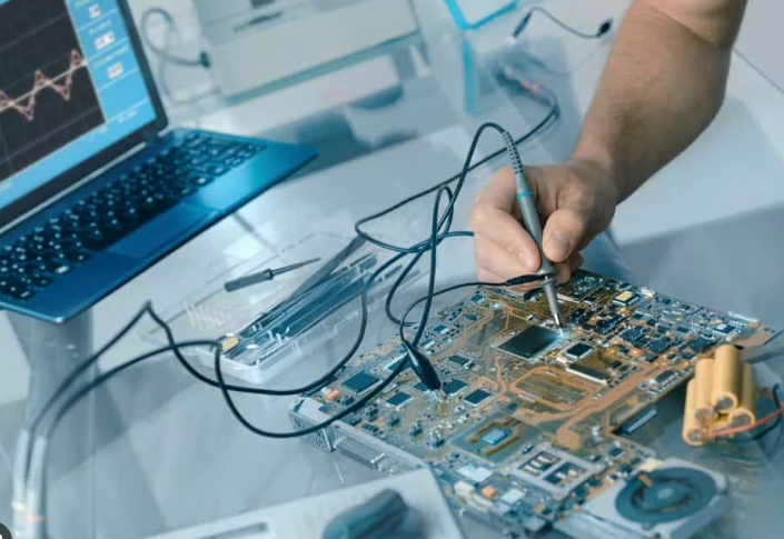
Turnkey Printed Circuit Board Assembly Process
1. Design and Verification: After customers submit design files (Gerber, BOM, component libraries), manufacturers conduct DFM (Design for Manufacturing) analysis. This includes checking layout rationality, compliance of line width/spacing (e.g., IPC-6012 standards), and thermal design optimization.
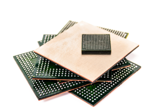
2. Material Procurement and Supply Chain Management: Based on the BOM, components and PCB substrates are procured from ISO 9001/14001 certified suppliers. An ERP system tracks material status to ensure traceability of critical components (e.g., BGA, CSP). Incoming materials undergo inspection, such as XRF testing for solder composition compliance.
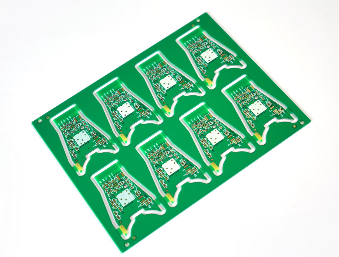
3. PCB Manufacturing and Lamination: Processes include layer stacking, etching, drilling, and plating, adhering to standards like IPC-6013 (flexible boards) or IPC-6012 (rigid boards).
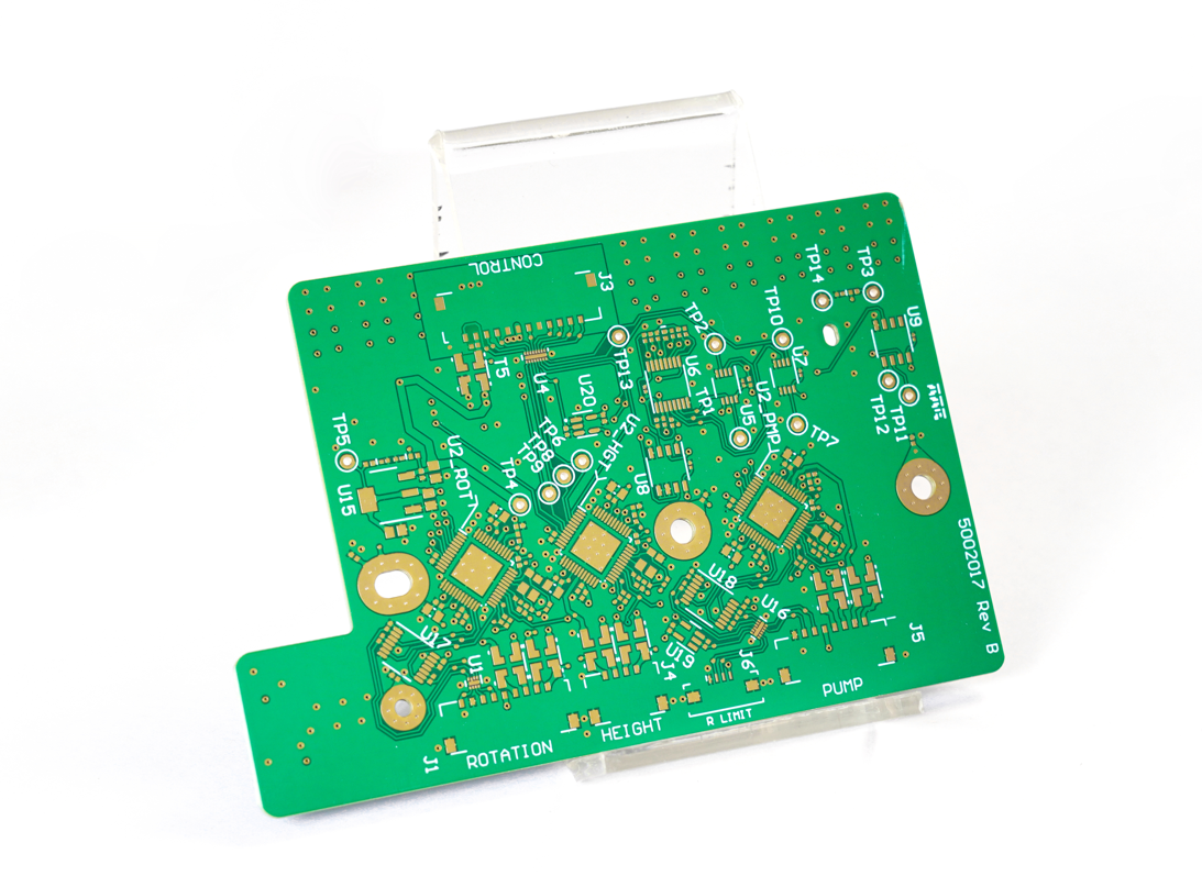
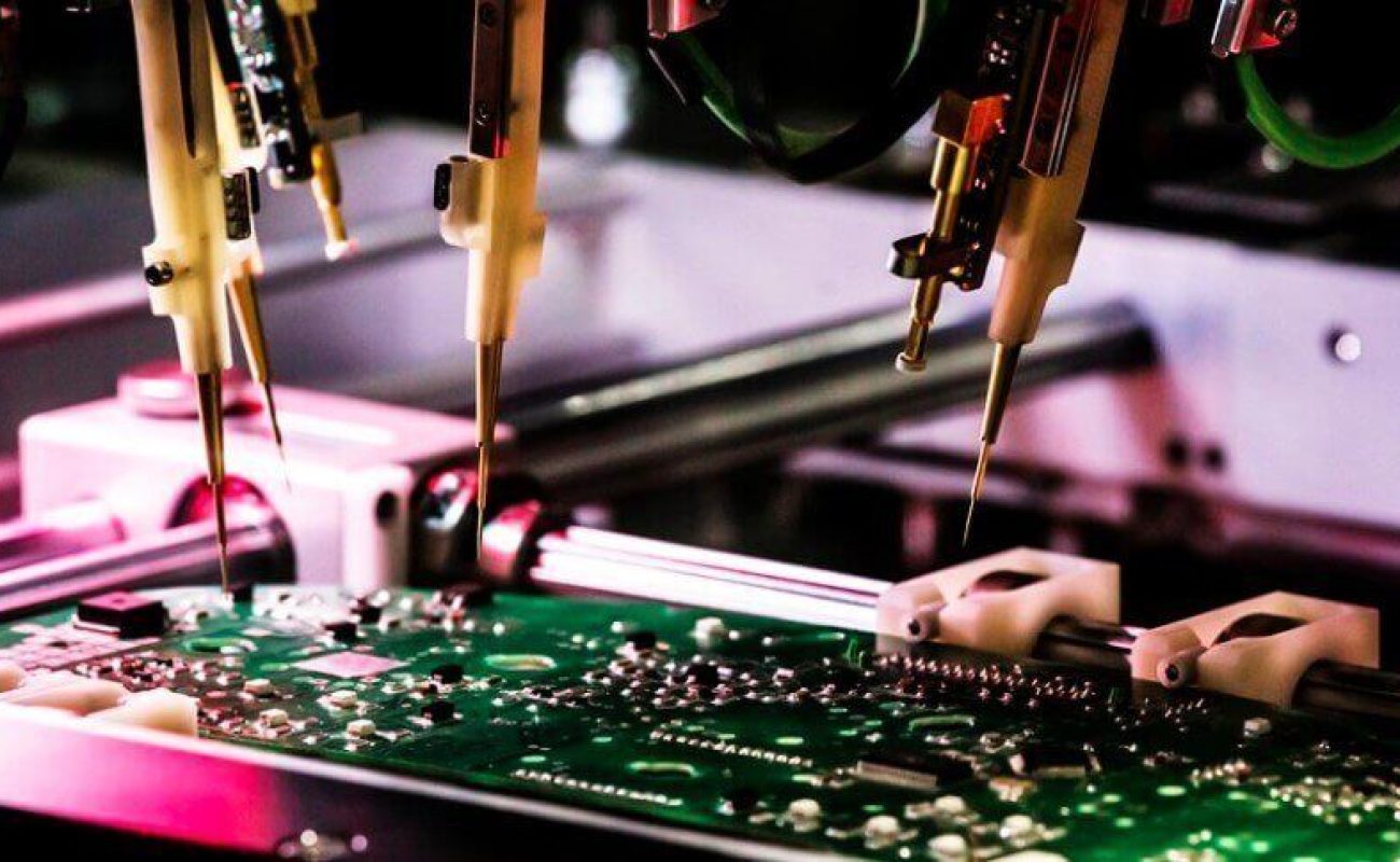
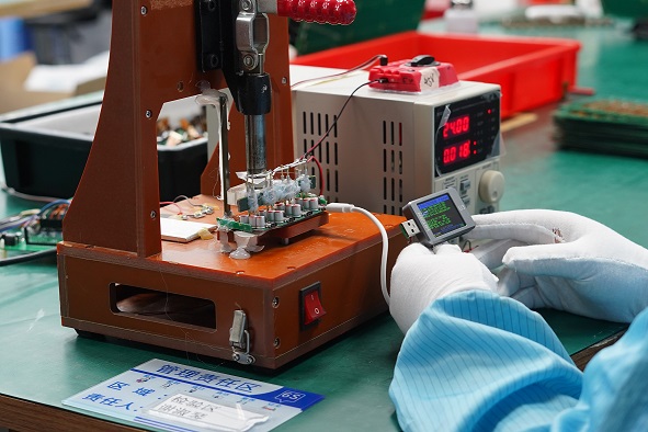
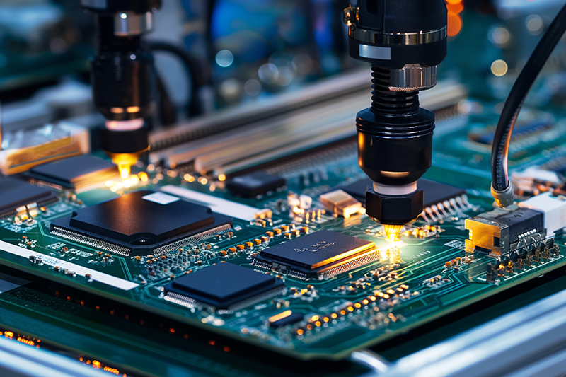
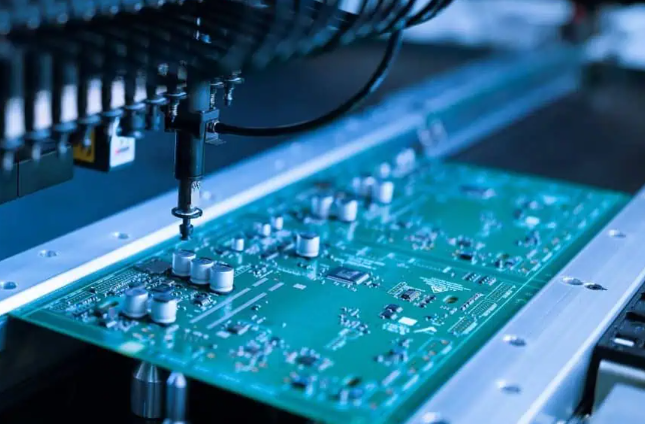
4. Surface Mount and Through-Hole Assembly: SMT production lines use high-speed placement machines (e.g., Siemens SIPLACE) for 0201 component placement with ±0.05mm accuracy. Through-hole components are assembled via wave soldering or selective soldering, combined with nitrogen protection to reduce oxidation.
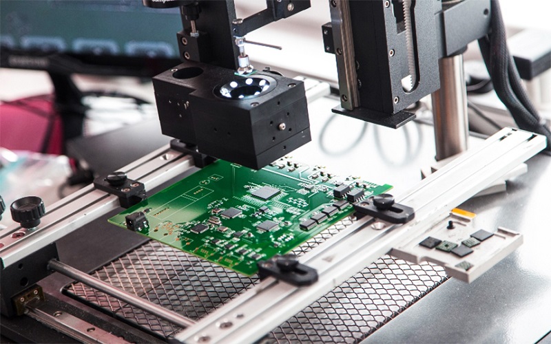
5. Soldering and Connection Processes: Reflow soldering is performed in a nitrogen environment to ensure solder joint reliability and gloss. BGA packages undergo X-ray inspection for solder ball integrity. Soldering temperature profiles strictly follow J-STD-001 standards to prevent cold soldering or thermal damage.
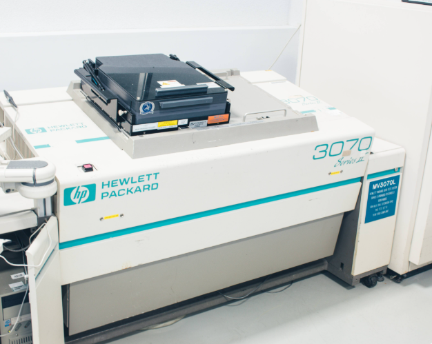
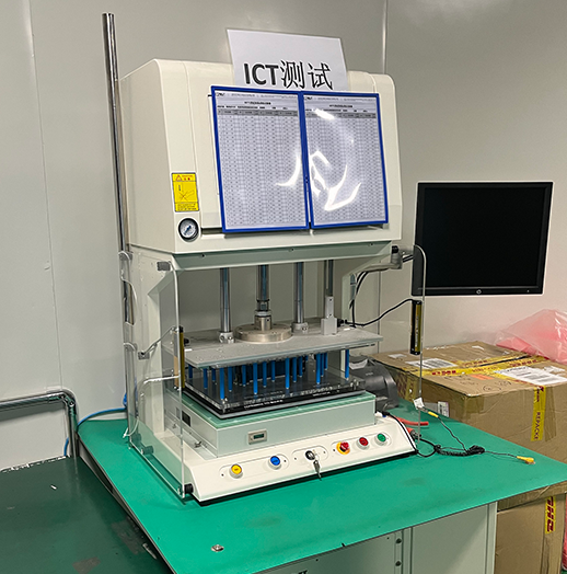
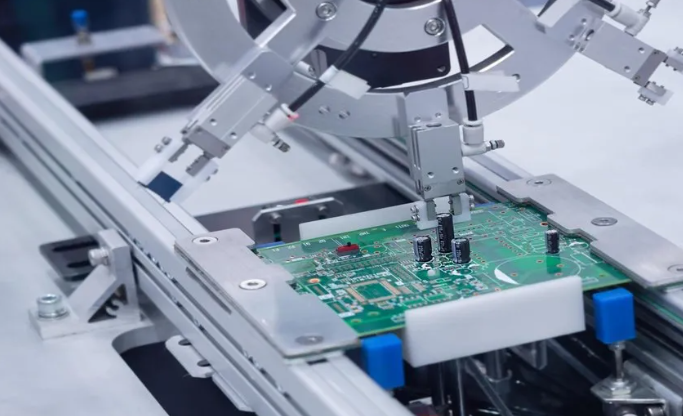
6. Multidimensional Testing and Quality Inspection: In-line AOI detects placement deviations. ICT (In-Circuit Testing) verifies circuit functionality, while flying probe testing covers over 99% of network nodes. Functional testing simulates real-world conditions (e.g., -40°C to 125°C thermal shock), and aging tests last 168 hours to validate long-term stability.
7. Quality Control System: Visual inspections follow IPC-A-610 standards. SPC (Statistical Process Control) monitors critical parameters like solder paste thickness. Manufacturers certified under ISO 13485 (medical devices) or AS9100 (aerospace) implement additional environmental stress screening (e.g., vibration testing).
8. Packaging and Logistics: ESD-safe packaging (e.g., conductive foam) and vacuum-sealed moisture barriers are used. Logistics integrate tracking systems to ensure global delivery timeliness, such as 48-hour delivery via DHL/FedEx partnerships.
9. Final Validation and Delivery: Finished products undergo final functional testing, generating traceable batch reports (including test data and QC signatures). After customer confirmation, products enter mass production, supporting seamless transition from small-batch trials to large-scale manufacturing.
10. After-Sales Support and Feedback Loop: Technical documentation (e.g., assembly guides, troubleshooting manuals) and on-site support services are provided. Continuous process optimization is driven by customer feedback, such as implementing AI-powered defect prediction systems to reduce repair rates below 0.1%.
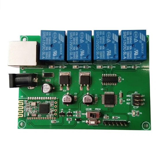
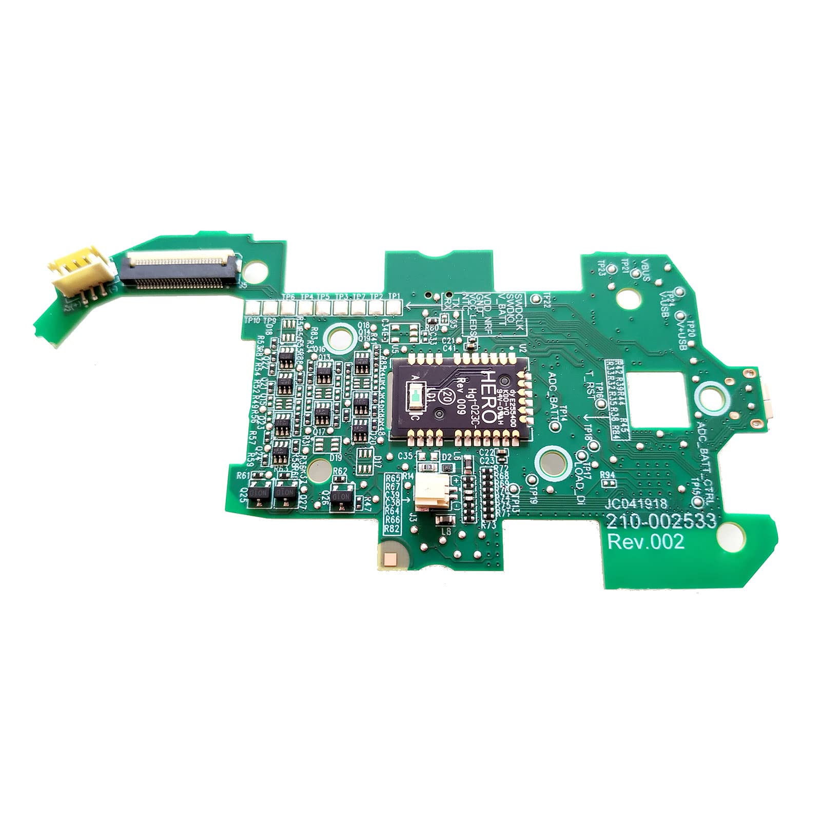
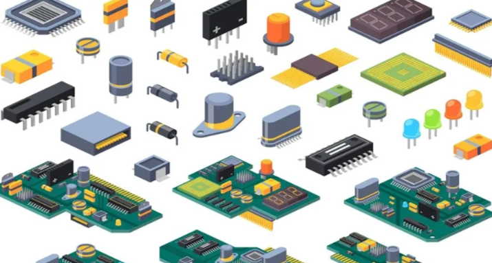
Turnkey PCB Assembly Types We Can Offer
- Surface mount technology (SMT): High-precision placement machines enable automated placement of micro-components (such as 0201 packages and 0.35mm pitch BGAs), making it suitable for high-density, miniaturized circuit boards (such as smartphone motherboards).
- Through-hole technology (THT): Wave soldering or hand soldering is used to mechanically secure and electrically connect large components (such as connectors and relays), making it suitable for applications requiring high mechanical strength (such as industrial power modules).
- Hybrid technology (SMT/THT): Combining SMT and THT processes, it is compatible with both surface mount and plug-in components and is suitable for complex circuit designs (such as double-sided PCBs or multilayer boards).
Why Choose EBest Circuit (Best Technology) as Turnkey PCB Assembly Services Supplier?
Reasons Why Choose us as Turnkey PCB Assembly Services Supplier:
- Global Top-Tier Certification Quality Assurance System: Achieved ISO 9001, ISO 13485 (Medical), and AS9100D (Aerospace) triple international certifications, enforcing end-to-end rigorous control from raw material procurement to final delivery. Solder composition is 100% traceable, BGA solder ball integrity verified via X-ray NDT, with defect rates capped at 0.1%, significantly outperforming industry benchmarks.
- Imported High-Speed SMT Mounting Capacity: Equipped with imported high-speed SMT machines, achieving ±0.05mm precision for 0201 components with 4 million SMT points/day + 3 million DIP points/day throughput. Supports seamless transition from small-batch (200PCS) prototyping to mass production (20K+), with standard lead time of 3 days and next-day express for urgent orders.
- Lead-Free Soldering Process & Extreme Reliability Verification: Adopts J-STD-001-compliant lead-free solder paste process with 245-260℃ peak temperature control and ≥3℃/s cooling rate. Passes 168-hour thermal shock aging tests, enhancing solder joint gloss by 20% while maintaining cold solder rates below 0.1%.
- Triple-Layer Inspection System for Full-Cycle Quality Control: AOI detects ±0.05mm placement deviations, ICT validates circuit functionality, and FCT simulates -40℃~125℃ extreme conditions. Flying probe tests cover 99% of net nodes with 99.9% signal integrity, ensuring zero-defect delivery.
- MES-Enabled Full-Lifecycle Traceability: MES production execution system tracks material lifecycle with XRF composition testing and batch traceability for critical components. SPC monitors key parameters like solder paste thickness (±0.01mm), stabilizing yield at ≥98%.
- Eco-Compliance & Cost Optimization: Complies with EU ROHS lead-free standards, reducing material costs by 10% through supply chain optimization. Combined with 85% full-line automation and high yield rates, overall project costs are 15% below industry averages.
- ESD Protection & Global 48-Hour Logistics Network: Uses conductive foam + vacuum-sealed anti-static packaging. Integrates with DHL/FedEx for global 48-hour door-to-door delivery, supporting flexible multi-batch/small-quantity distribution.
Our Turnkey PCB Assembly Capabilities
| Item | Capabilities |
| Placer Speed | 13,200,000 chips/day |
| Bare Board Size | 0.2″ × 0.2″ – 20″ × 20″ / 22″ × 47.5″ |
| Minimum SMD Component | 01005 (0.4mm × 0.2mm) |
| Minimum BGA Pitch | 0.25mm (10mil) |
| Maximum Components | 50mm × 150mm (Board Area) |
| Assembly Type | SMT / THT / Mixed Assembly |
| Component Package | Reels / Cut Tape / Tube / Tray / Loose Parts |
| Lead Time | 1 – 5 days (Standard) |
How to Get a Quote for Turnkey PCB Assembly Services?
Quotation Submission List for Turnkey PCB Assembly Services:
- BOM (Bill of Materials): Excel/.xlsx/.csv, detailing component name, model, quantity, package type (SMT/THT), supplier, and specifications (e.g., 0603 resistor, SOP-8 package).
- Gerber Design Files: Copper layer, solder mask layer, silkscreen layer, solder paste layer, and NC drill files in RS-274X format.
- Centroid File (Pick-and-Place Coordinate File): Component coordinates, rotation angles, and reference designators for SMT machine programming and process validation.
- PCB Engineering Drawings & Design Documents: Schematics, PCB layout diagrams, assembly drawings, and 3D models (e.g., STEP files) to specify hole positions, dimensions, connector placements, and special assembly requirements (e.g., waterproof coating, thermal design).
- Testing & Certification Requirements: Test Specifications: ICT (In-Circuit Test), FCT (Functional Circuit Test), burn-in testing, X-ray inspection (for BGA/CSP), etc.
- Certification Documents: RoHS, CCC, ISO, and other environmental/safety compliance requirements; specify lead-free process compliance.
- Production Quantity & Lead Time: Define order quantities (e.g., small batch: 10-500pcs; bulk: 500+pcs) and delivery timelines (e.g., 8-48 hours for rapid prototyping, 1-2 weeks for mass production), which directly influence cost structure and production scheduling.
Welcome to contact us if you have any request for turnkey PCB assembly: sales@bestpcbs.com.