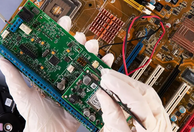
What is water level indicator PCB? Let’s explore its definition, components, types, design guide and layout technique and recommended manufacturer.
Are you worried these issues about water indicator PCB?
- Does water level indicator PCB corrode rapidly in humid environments? Do you require corrosion resistance beyond standard specifications?
- Are frequent design iterations causing uncontrolled costs? Are you facing hidden cost escalation with each design revision?
- Do design flaws lead to production rework? Do you need proactive risk mitigation through design validation?
As a water level indicator PCB manufacturer, EBest Circuit (Best Technology) can provide you service and solution:
- Enhanced Corrosion Resistance: Weather-resistant substrate +conformal coating technology delivers 3x corrosion resistance in humid/saline environments, ensuring 5-year stable operation.
- Modular Circuit Optimization: 20% reduction in component count, 15% cost savings, and ±0.3% precision control through standardized design architecture.
- Complimentary DFM Design Audit: Expert team conducts manufacturability analysis from design to production, identifying 90% of potential production risks upfront, reducing trial production time by 30% for seamless production readiness.
Feel free to contact us if you have any inquiry for water level indicator PCB: sales@bestpcbs.com.
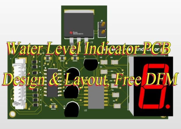
What Is Water Level Indicator PCB?
The Water Level Indicator PCB is a printed circuit board designed for real-time monitoring, display, and control of liquid levels. It typically integrates components such as capacitive, ultrasonic, or liquid level sensors, LED/LCD display screens, buzzers, and control circuits.
Its primary function is to detect liquid height through sensors, convert physical water level signals into electrical signals, process them digitally, and present water level values or statuses (such as 0-9 digital displays, low/high alerts) via display modules. It can also connect to relays, motors, or other actuators to enable automatic water replenishment or overflow protection.
Widely used in household water tanks, industrial storage tanks, agricultural irrigation systems, and environmental monitoring, this device offers high precision, scalability, energy efficiency, and water conservation, serving as a fundamental hardware platform for intelligent water management.
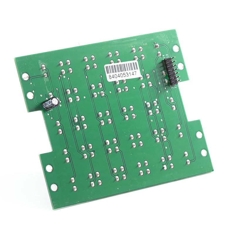
Components of Water Level Indicator PCBs
- Sensor Module: Includes capacitive/ultrasonic/liquid level sensors and multi-stage probes (e.g., 9-point water level probes). It detects water levels through conductive media or acoustic reflection principles, enabling continuous or discrete level identification from empty to full tanks.
- Display Module: Utilizes seven-segment displays, LCD/LED screens, or 0.96-inch OLED screens to visually present real-time water level values (e.g., 0-9 digits), statuses (empty/full alerts), and environmental parameters (e.g., temperature/humidity). Some designs support dynamic graphical interfaces.
- Control Core: Centers on microcontrollers (e.g., STM32F103C8T6, 51 MCU, AVR series) paired with components like BC337 transistors and 330Ω resistors. It processes signals, executes logic judgments, and outputs instructions—for example, identifying the highest water level via priority encoders to drive displays.
- Alarm Unit: Integrates active buzzers and LED indicators. When water levels reach preset thresholds (e.g., full or empty), it triggers audible and visual dual alarms for timely user intervention.
- Actuator Module: Controls pumps, motors, or solenoid valves via relays to enable automatic water replenishment, overflow protection, or dry-run prevention. For instance, it activates pumps at low water levels and cuts power at high levels to prevent spills.
- Power Management: Operates on 5V DC power or rechargeable batteries, combined with voltage-stabilizing circuits to ensure stable system operation. Some designs incorporate low-power modes to extend battery life.
- Communication Module: Optionally equipped with WiFi, NB-IoT, or MQTT modules to transmit data to cloud platforms or mobile apps for remote monitoring, threshold setting, and abnormal alert notifications.
- Auxiliary Components: Include temperature/humidity sensors (for environmental monitoring), keypads (for manual mode switching/device reset), PCB substrates (to mount all electronic components), and connectors (for circuit interface expansion), ensuring system completeness and scalability.
Types of Water Level Indicator PCB
Electrode-Type Water Level Meter PCB
- Principle: Employs a common electrode to emit PWM pulses, generating voltage changes on secondary electrodes. ADC voltage sampling detects water level.
- Features: Supports MODBUS RTU protocol, configurable trigger thresholds for varying water quality environments, and includes RS485 communication with network capabilities like MQTT protocol.
- Application: Industrial boilers, pressure vessels, household appliances (e.g., water heaters, humidifiers).
Wireless Water Pump Controller PCB
- Principle: Uses an RF module and logic gates (e.g., CD4001 NOR gate) to construct a wireless control circuit, enabling automatic pump start/stop via water level thresholds.
- Features: Low cost (~$3–4), wire-free installation suitable for remote water level monitoring and pump coordination.
- Application: Household water tanks, agricultural irrigation requiring wireless control.
IoT Water Quality Monitoring Buoy PCB
- Principle: Integrates low-power sensors (e.g., pH, temperature, dissolved oxygen) with NB-IoT modules for real-time cloud data uploads.
- Features: Enables high spatiotemporal resolution monitoring, includes GPS positioning and Bluetooth diagnostic functions, with cost below $1,000.
- Application: Pollution monitoring in flowing water bodies like rivers and lakes.
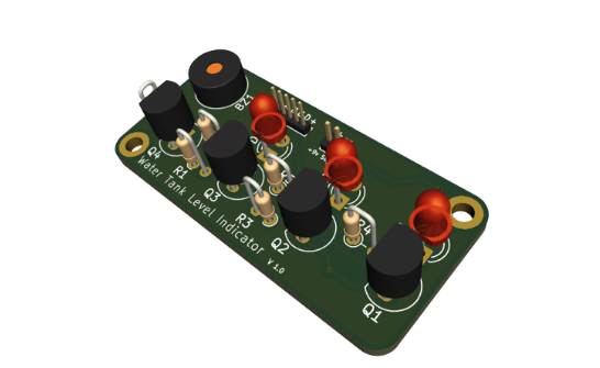
Simple Water Level Indicator PCB
- Principle: Implements high/low water level alarms using basic circuits (e.g., buzzers, logic gates).
- Features: Simple structure, low cost, but functionally limited, typically lacks communication capabilities.
- Application: Small water tanks, simple water storage equipment.
Water Level Indicator PCB Design for Manufacturability Guide
A Detailed Manufacturability Guide for Water Level Indicator PCB Design:
1. Layout Optimization and Modular Partitioning
- Functional Module Physical Isolation: Partition water level sensor arrays, signal conditioning circuits, MCU control modules, and power management units with spacing ≥5mm. High-frequency clock lines (e.g., SPI buses) and analog sensor signal lines maintain ≥10mm spacing to prevent crosstalk. Capacitive sensor electrodes must align with PCB edges, with electrode spacing error ≤±0.1mm for precise capacitance coupling.
- Advanced Routing Rules: High-speed signals use microstrip design with 50±5Ω impedance control. Differential pairs maintain width error ≤±0.02mm and spacing error ≤±0.05mm. Power plane segmentation employs “thermal isolation” techniques, with copper mesh density ≥30% under power devices for heat dissipation.
- EMC Enhancement: Critical sensitive circuits (e.g., low-noise amplifiers) are surrounded by shielding enclosures with grounding pads spaced ≤3mm. Power entry points incorporate π-type filter networks (10μF electrolytic capacitor + 10nF ceramic capacitor + ferrite bead) to suppress conducted noise.
2. Material Selection and Performance Matching
- Substrate Grading Applications: Consumer-grade scenarios use FR-4 (Tg130℃, Dk=4.3-4.5, Df=0.018). Industrial-grade applications adopt high-Tg FR-4 (Tg170℃) or polyimide (PI, Tg≥250℃). High-frequency scenarios (e.g., radar level gauges) utilize RO4350B (Dk=3.48, Df=0.003) or PTFE substrates (Dk=2.9-3.0, Df=0.001).
- Copper Thickness Dynamic Selection: Signal layers use 0.5oz (17μm) copper, power layers use 2oz (70μm) copper. High-current paths (e.g., relay drives) require impedance calculations, line width ≥3mm, copper thickness ≥3oz, and temperature rise ≤20℃.
- Surface Finish Process Comparison: ENIG thickness 2-5μm suits fine-pitch pads. OSP thickness 0.2-0.5μm offers low cost but poor thermal stability. ENEPIG suits high-frequency scenarios with contact resistance ≤5mΩ.
3. Solder Mask and Silkscreen Specifications
- Solder Mask Opening Control: Sensor contact areas have solder mask openings 0.3mm larger than pads to avoid capacitance detection interference. BGA pads adopt NSMD design with solder mask opening diameter = pad diameter + 0.1mm.
- Standardized Silkscreen Identification: Component labels use 2mm sans-serif font. Polarized components display “+” symbols ≥2mm×2mm. Test points are labeled “TP_01”, “TP_02” etc., with font height ≥1.5mm. Version numbers are placed in PCB blank areas with font height ≥3mm.
- Mechanical Positioning Reinforcement: Mounting holes use plated through-holes with diameter error ≤±0.1mm and wall copper thickness ≥25μm. Locating pin holes maintain ≥5mm spacing from PCB edges to prevent edge stress-induced cracks.
4. Test Point Design Standards
- Test Point Layout Strategy: Test points are grouped by functional modules. Power test points cluster at power entry points, signal test points distribute at critical nodes (e.g., MCU outputs). Test point spacing ≥3mm prevents simultaneous probe contact.
- Electrical Characteristic Verification: Test points maintain ≥0.8mm spacing from adjacent signal lines to avoid short circuits during testing. Critical test points (e.g., power, ground) require dedicated test pads ≥2mm×2mm, avoiding substitution with component pads.
- Solder Mask Opening Optimization: Test point solder mask openings are 0.3mm larger than pads to ensure post-soldering exposure. Test points receive ENIG treatment for ≤10mΩ contact resistance.
5. Design for Manufacturability (DFM) Verification Checklist
- Electrical Rule Check (DRC) Deepening: DRC settings include minimum line width 0.15mm, minimum spacing 0.15mm, and minimum via 0.2mm/0.4mm (hole/pad). Power and ground plane spacing ≥0.2mm prevents short-circuit risks.
- File Integrity Verification: Confirm Gerber files include all layers (top, bottom, inner layers, solder mask, silkscreen) with version matching BOM tables. Check drill files (Excellon format) align with mechanical layer positioning holes to avoid assembly deviations.
- Process Feasibility Assessment: Confirm PCB manufacturer capabilities for minimum line width/spacing, minimum via, and minimum blind/buried vias. Evaluate compatibility for board thickness (0.8-3.2mm), copper thickness (0.5-3oz), and surface finishes (ENIG/OSP/ENEPIG).
6. Environmental Adaptability Design
- Temperature Cycle Tolerance Enhancement: For -40℃ to 125℃ thermal cycling tests, select substrates with CTE ≤12ppm/℃ (e.g., ceramic-filled PTFE). High-humidity environments (RH≥85%) use substrates with water absorption ≤0.05% (e.g., Teflon FEP).
- Mechanical Strength Improvement: In vibration scenarios (e.g., automotive applications), use 0.8mm thick PCB + 1mm thick stiffener (FR-4 or aluminum substrate) connected via 0.5mm diameter plated through-holes. Board edges adopt R-angle design with R≥2mm to avoid stress concentration.
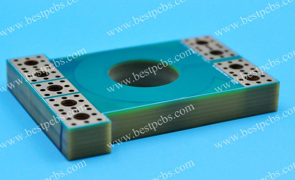
- Corrosion Protection Expansion: In coastal or chemical environments, apply conformal coatings (e.g., Parylene) at 20-50μm thickness. Critical solder joints receive waterproof adhesive (e.g., silicone) sealing for IP67 waterproof rating.
7. Signal Integrity and EMI Control
- Impedance Matching Deepening: High-speed signal lines use microstrip design with 50±5Ω impedance, adjusted via line width/spacing. Differential pairs maintain 100±10Ω impedance with tight coupling (spacing ≤2× line width). Critical signal lines (e.g., clock lines) employ ground shielding (Ground Guard) ≥3× line width.
- Filter Design Optimization: Power entry points use LC filter networks (10μF electrolytic capacitor + 100nF ceramic capacitor + 10μH inductor) to suppress low-frequency noise. Sensor signal lines incorporate ferrite beads (impedance ≥60Ω@100MHz) to suppress high-frequency noise.
- Ground Plane Segmentation Refinement: Analog and digital grounds connect via single-point grounding (Star Ground) using 0Ω resistors or beads. Large ground planes require solder mask bridges (width ≥0.5mm) to prevent cracking during soldering. Ground plane and signal line spacing ≥0.3mm avoids parasitic capacitance.
Best Practice for Water Level Indicator PCB Layout
Below Are Optimization Methods About Water Level Indicator PCB Layout:
1. Sensor Interface Optimization Layout
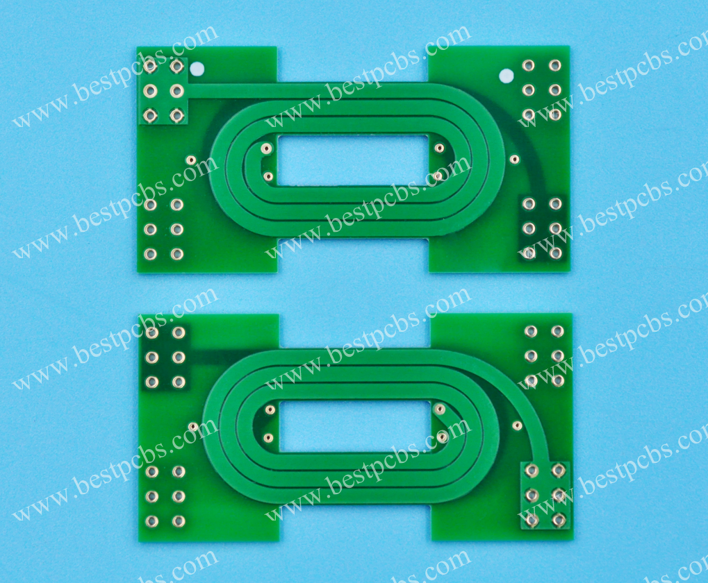
- Copper Foil Shape and Size Optimization: Use trapezoidal or serrated elongated copper traces (contact area from 4×4mm to 30×30mm) instead of thick copper pillars/pipes to minimize parasitic capacitance. Recommended trace width ≤1.5mm to reduce electric field coupling effects.
- No-Copper Zone Expansion: Prohibit components or traces within 3mm behind the sensor and apply insulating tape/coating to prevent capacitive coupling. Maintain a 5mm clearance zone around critical sensor areas.
- Capacitor Parameter Precision: Use X7R/NPO dielectric material SMD capacitors (accuracy ≥10%). Place C1 and CDC capacitors adjacent to the IC, ensuring 2×CDC > CIN2 channel capacitance (15pF baseline). Configure multiple capacitance values (e.g., 10pF, 22pF) for sensitivity adaptation.
2. Signal Integrity Protection Strategy
- Functional Partition and Isolation Enhancement: Separate high-speed digital signals (e.g., SPI/I2C buses) and low-speed analog signals (sensor circuits) via physical isolation strips or grounded shielding layers (≥1mm width). Use shielded traces or differential pairs for critical analog signals like ADC inputs.
- Differential Routing and Impedance Control: Implement differential routing for critical signals (e.g., USB, LVDS) with length matching error <0.1mm and spacing ≥3× trace width. Verify impedance matching (50Ω±10%) via 2D field solvers. Replace 90° corners with 45° miters or arcs for high-frequency traces.
- Ground Plane Optimization: Maintain a continuous ground plane connected across layers via thermal via arrays (≥20 vias/cm²). Single-point connect analog and digital grounds at the power entry point to avoid ground loops.
3. EMC Protection Design
- Physical Isolation and Shielding: Maintain ≥0.5m distance between sensors and strong interference sources (e.g., VFDs, motor drives) or use twisted-pair shielded cables (120Ω±20Ω impedance) with ferrite beads (1-30MHz attenuation ≥20dB). Cover sensitive circuit areas with grounded copper shields.
- Power Domain Partitioning and Decoupling: Segment power domains using ferrite beads/0Ω resistors. Implement 10nF ceramic + 10μF electrolytic capacitor decoupling networks (placement ≤3mm). Add π-type filtering (inductor + capacitor) at power entry points to suppress ripple (<50mV).
4. Thermal Management Solutions
- High-Power Device Placement and Heat Dissipation: Position LDOs/power amplifiers near PCB edges or heat sinks. Use ≥2oz copper thickness with thermal via arrays (≥10 vias/cm²) and apply thermal paste/heatsinks (thermal conductivity ≥2W/m·K).
- Substrate Selection and Thermal Simulation: Utilize metal-core (aluminum/copper) or ceramic (Al₂O₃/AlN) substrates for enhanced thermal diffusion. Validate temperature rise ≤30°C via thermal simulation tools (e.g., ANSYS Icepak).
5. Waterproofing and Reliability Enhancement
- Sealing and Material Selection: Use IP67-rated connectors and apply conformal coatings (acrylic/silicone) or potting compounds (low dielectric constant preferred). Prevent glue intrusion into sensor probes by reserving air gaps to avoid dielectric constant changes causing false triggers.
- Reliability Testing: Conduct accelerated life tests including temperature-humidity cycling (-40℃~125℃, 1000 cycles), vibration testing (5G peak acceleration, 2 hours), and salt spray testing (5% NaCl, 96 hours) to ensure MTBF ≥50000 hours. Validate solder joints via X-ray inspection and pull tests.
6. Power and Grounding System Design
- Power Path Optimization and Ripple Suppression: Use short wide traces (≥2mm width) with star topology to minimize voltage drop (<100mV). Implement π-type filtering at power entry points. Isolate digital noise for sensitive analog circuits using dedicated LDOs.
- Grounding System and Noise Suppression: Single-point connect analog and digital grounds at the power entry point. Use dedicated ground planes and magnetic beads for critical circuits (e.g., ADC) to suppress high-frequency noise (1MHz-100MHz attenuation ≥20dB).
7. Maintainability and Manufacturing Friendliness
- Test Point Standards and Debug Interfaces: Space test points ≥2.54mm apart with clear labeling. Include debug interfaces (e.g., UART, I²C) with 0Ω resistor jumpers for in-circuit debugging. Add voltage monitoring points for real-time measurement.
- Standardized Packaging and Production Files: Use standardized packages (0805 resistors, SOT-23 transistors) for automated assembly and AOI inspection. Generate complete BOMs (part numbers, footprints, suppliers) and Gerber files. Include process edges (≥3mm width) for SMT precision (±0.1mm). Implement temperature curve monitoring and SPC control for key processes (reflow, wave soldering).
Why Choose EBest Circuit (Best Technology) as Water Level Indicator PCB Manufacturer?
Reasons to Choose EBest Circuit (Best Technology) as Your Water Level Indicator PCB Manufacturer:
- Cost Optimization Leadership: Leverage economies of scale and strategic material sourcing to deliver PCB solutions with 8-12% lower costs than industry averages, particularly through cost-sensitive design adaptations like FR4 material substitution achieving 20% cost reduction without compromising functionality.
- Free DFM: Complimentary DFM analysis by seasoned engineers with 19+ years’ expertise identifies design flaws early, reducing ECO iterations by 30% and accelerating time-to-market while minimizing trial production expenses.
- Rapid Prototyping Capability: 24-hour turnaround for urgent samples via dedicated priority lanes and intelligent production scheduling, enabling 40% faster prototyping compared to standard industry timelines.
- Reliable Delivery Performance: 99.2% on-time delivery rate achieved through real-time MES production monitoring and streamlined logistics, ensuring supply chain stability and preventing market opportunity losses.
- Stringent Quality Control: Comprehensive batch inspection system with AOI optical verification and electrical testing under rigorous quality protocols, maintaining defect rates below 0.08% for superior product longevity.
- 19-Year Process Intelligence: Proprietary database of 5000+ manufacturing cases and error patterns enables predictive risk mitigation, such as solder pad design optimization, reducing rework costs by 15%.
- End-to-End Technical Support: Dedicated engineers provide continuous process improvement guidance from NPI to mass production, including signal integrity optimization for extended product lifecycle.
- Eco-Compliant Production: RoHS-certified materials ensure global regulatory compliance, eliminating legal risks associated with hazardous substances.
- Integrated Manufacturing Services: Full-spectrum solutions from rapid prototyping to volume production minimize vendor coordination efforts, enhancing supply chain efficiency by 20%.
- After-Sales Service Excellence: Lifetime technical support with 24/7 response capability, including free troubleshooting assistance and warranty extensions for mission-critical applications.
Our Quality Inspection for Water Level Indicator Circuit Board
Visual & Structural Inspection
- Printed Circuit Check: Verify no short circuits, open circuits, burrs, or line width/spacing deviations from design specifications.
- Pad & Solder Joint Quality: Inspect for full, smooth solder joints without cold solder, false solder, bridging, or excess/insufficient solder; pads must be free of lifting, peeling, or oxidation.
- Component Installation: Confirm correct model, specification, polarity, and placement of components (e.g., resistors, capacitors, chips, probe connectors); SMT components should show no displacement, floating, or tilting.
- Board Body & Coating: Ensure PCB surface is flat, with no delamination, blistering, scratches, or stains; solder mask (green oil) coverage is uniform, and markings are legible.
Electrical Performance Testing
- Pre-Power Insulation Resistance Test: Use a megohmmeter to measure insulation resistance between power lines and ground, and between different polar lines, ensuring compliance with safety standards (typically ≥100 MΩ).
- Power-On Functional Test: Apply rated voltage, simulate varying water levels, and verify LEDs/other indicators illuminate/extinguish per logic, with no abnormal flickering or failure.
- Current & Power Consumption Test: Measure static and operational current values to confirm power consumption is within design limits, with no abnormal power drain or short-circuit currents.
- Signal Integrity Test: For digital/analog signal processing, check key waveforms (e.g., clock, sensor signals) for overshoot, ringing, or excessive delay.
Environmental Adaptability & Reliability Verification
- Thermal Cycling Test: Subject PCB to multiple temperature cycles (e.g., -10°C to +60°C) to confirm functionality and no component/joint cracking.
- Humidity Resistance Test: Expose to high-humidity environments (e.g., 40°C, 93% RH) for a specified duration; post-test functionality must remain intact with no corrosion or insulation degradation.
- Vibration & Shock Resistance: Simulate transport/usage vibrations/impacts to confirm no component loosening, detachment, or functional instability.
Critical Component & Water Environment Specialized Tests
- Water Level Sensor Interface Test: Verify sensor connectors/probes exhibit low contact resistance, reliable conductivity, and sensitive response to water level changes.
- Waterproofing & Sealing Verification (if applicable): For waterproof areas/connectors, perform seal tests to prevent moisture ingress causing shorts/corrosion.
- Material Corrosion Resistance: Evaluate PCB substrates, solder, and coatings for corrosion resistance in humid/aqueous environments.
Compliance & Documentation Review
- Industry Standard Compliance: Confirm PCB design/production meets relevant standards (e.g., IPC-A-600).
- Consistency Check: Compare actual PCBs against design drawings and Bill of Materials (BOM) to ensure full compliance.
- Inspection Record Archiving: Document all test data/results in a traceable quality report.
How to Get A Quote for Water Level Indicator PCB Project?
Material List Required For Water Level Indictor PCB Project Quote:
- PCB Dimensions: Specify exact length and width (e.g., 100mm×150mm) with tolerance requirements
- Layer Configuration: Single-layer/double-layer/multi-layer selection with interlayer thickness standards
- Substrate Parameters: FR-4 material type, board thickness (e.g., 1.6mm), copper foil thickness requirements
- Surface Treatment Process: HASL/ENIG/OSP selection with environmental grade specifications
- Solder Mask and Silkscreen: Color specification (e.g., green solder mask + white silkscreen) and coverage area
- Drilling Standards: Through-hole/blind via/buried via specifications with hole diameter accuracy (e.g., ±0.1mm)
- Component List: Include electronic component models, parameters, and quantities (e.g., LED indicators, sensor interfaces)
- Design Documents: Provide essential design files such as Gerber files and BOM lists
- Testing Requirements: Functional testing, burn-in testing, waterproof rating (e.g., IP67) and other validation items
- Delivery Lead Time: Specify sample delivery time and bulk production cycle
- Minimum Order Quantity: State MOQ and corresponding unit price
- Payment Terms: Advance payment ratio, final payment conditions, and invoice type
- Packaging Standards: Anti-static packaging, packing quantity, and outer box labeling requirements
- Certification Requirements: Necessary certifications such as CE, RoHS, etc.
Welcome to contact us if you have any request for water lever indicator PCB: sales@bestpcbs.com.