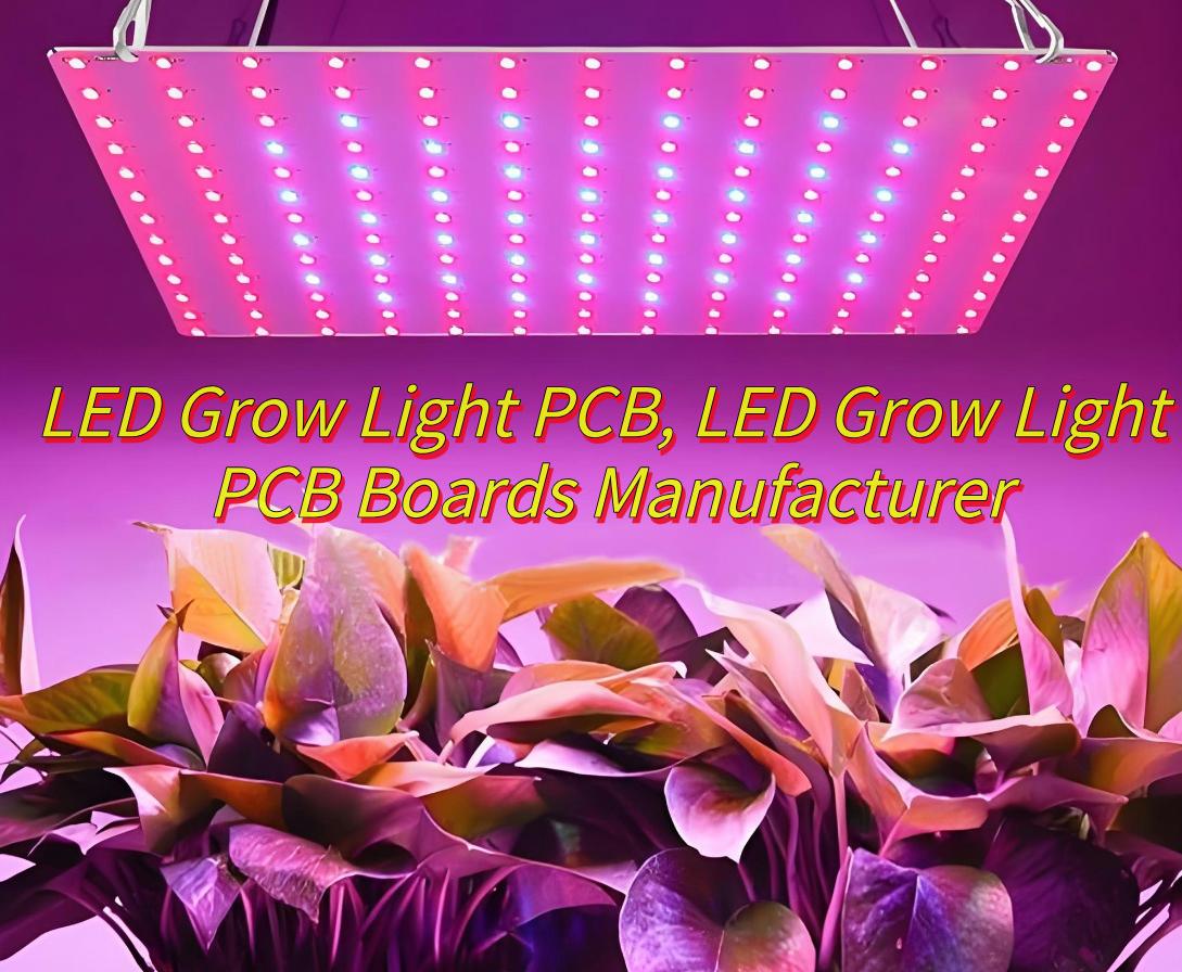
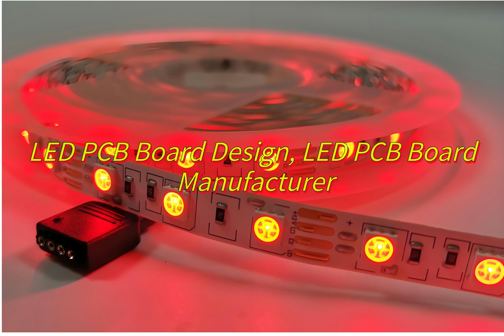
What is HASL Lead Free 94V0 LED PCB?
A HASL lead free 94V-0 LED PCB is a printed circuit board that designed for LED lightings, while coating with HASL lead free surface treatment and meet the 94V-0 flame retardant standard. HASL, full name is Hot Air Solder Leveling, it is a cost-effective surface finish used in the PCB manufacturing process. In the HASL lead-free process, the traditional lead-based soldering is replaced with a lead-free solder material, which is in line with environmental regulations like RoHS.
The 94V0 rating refers to the flame retardant standard of the PCB material, usually indicating that the material will not catch fire easily and can withstand higher temperatures. For LED PCBs, this is particularly important as LED devices can generate significant heat. The combination of lead-free HASL and 94V0 flame retardant material creates a reliable, durable, and environmentally safe solution for LED circuit boards. These types of PCBs are typically used in consumer LED lighting, display systems, and other applications that require low toxicity, high reliability, and long service life.
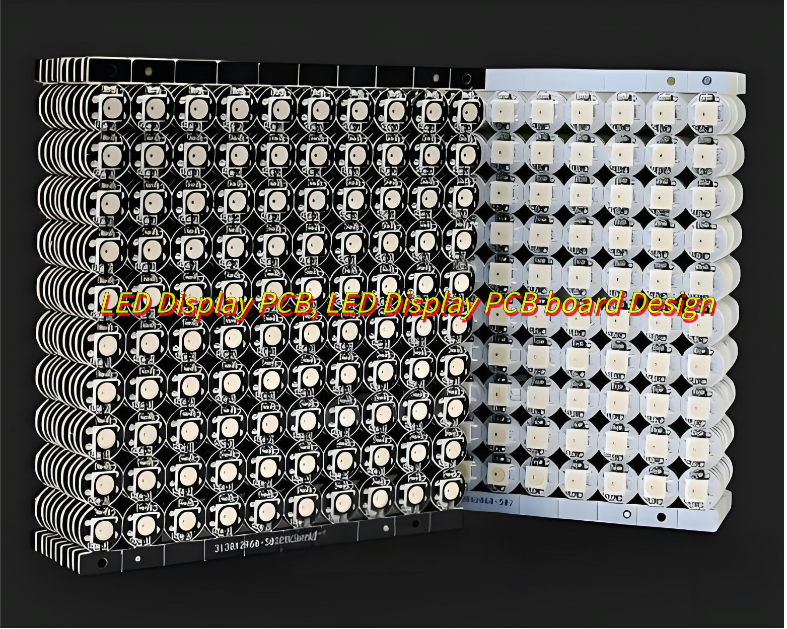
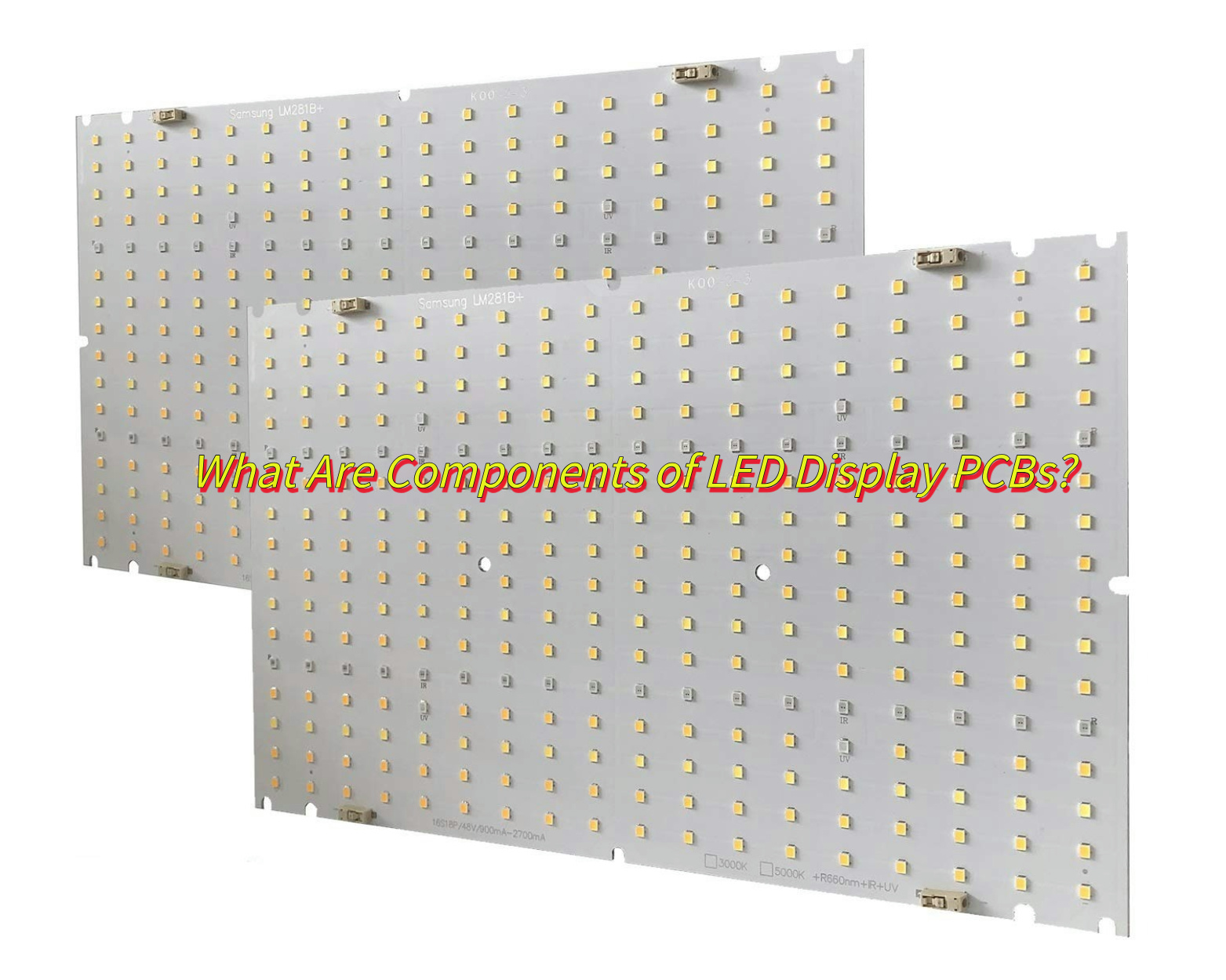
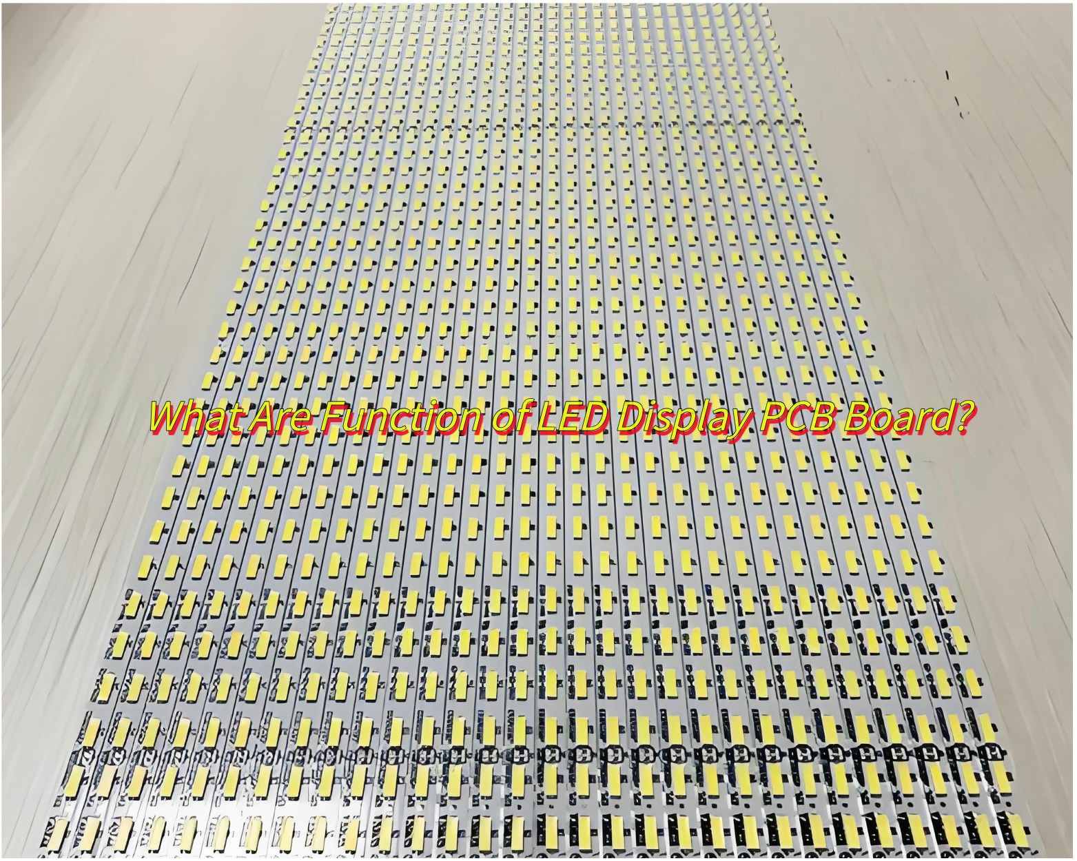
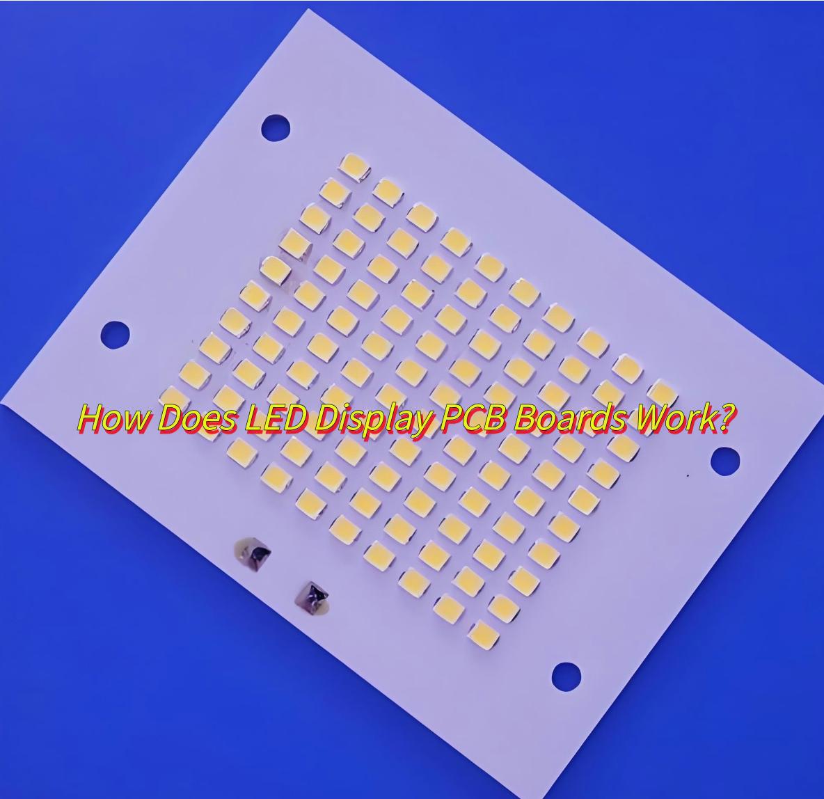
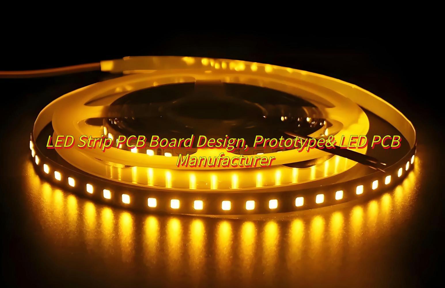
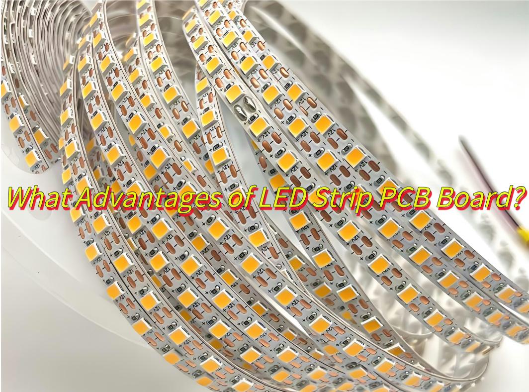
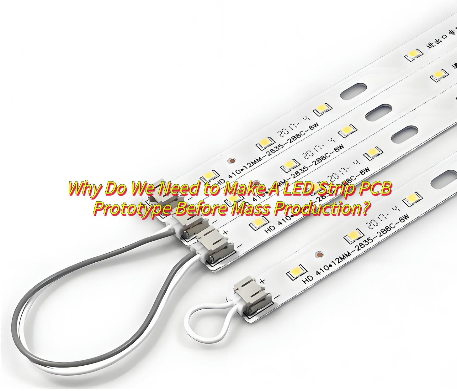
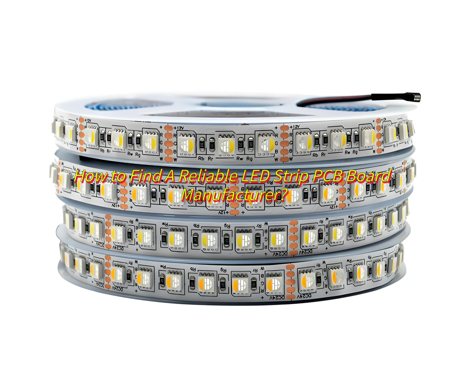
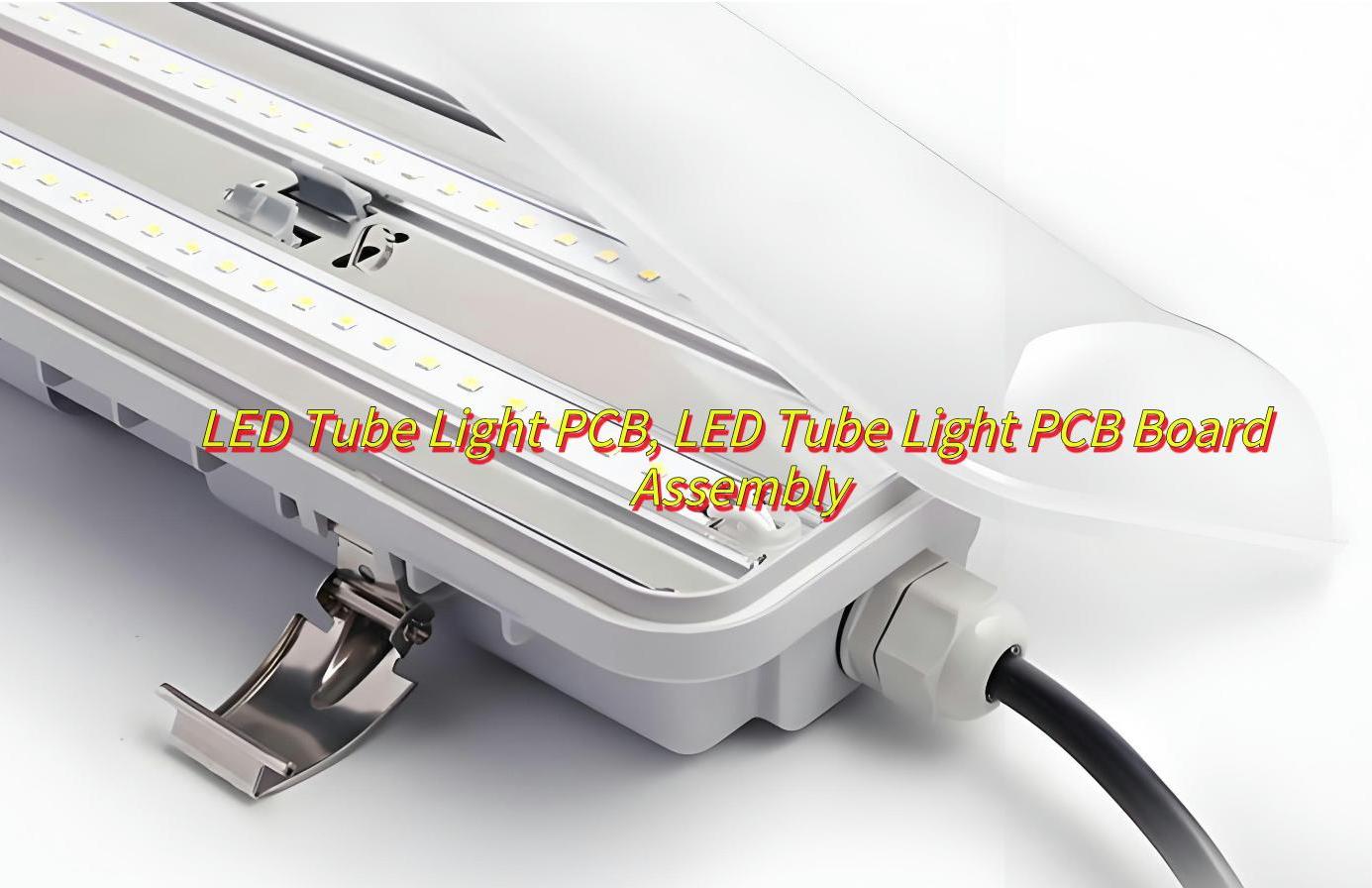
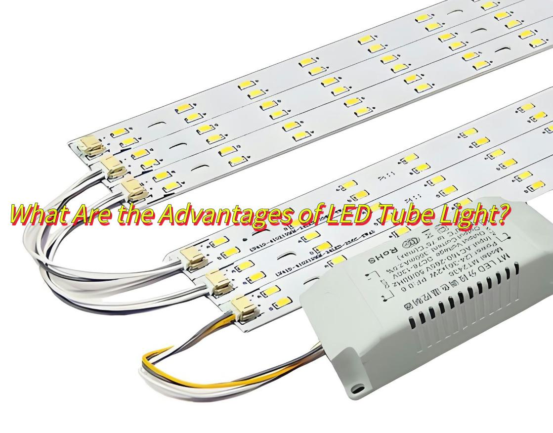
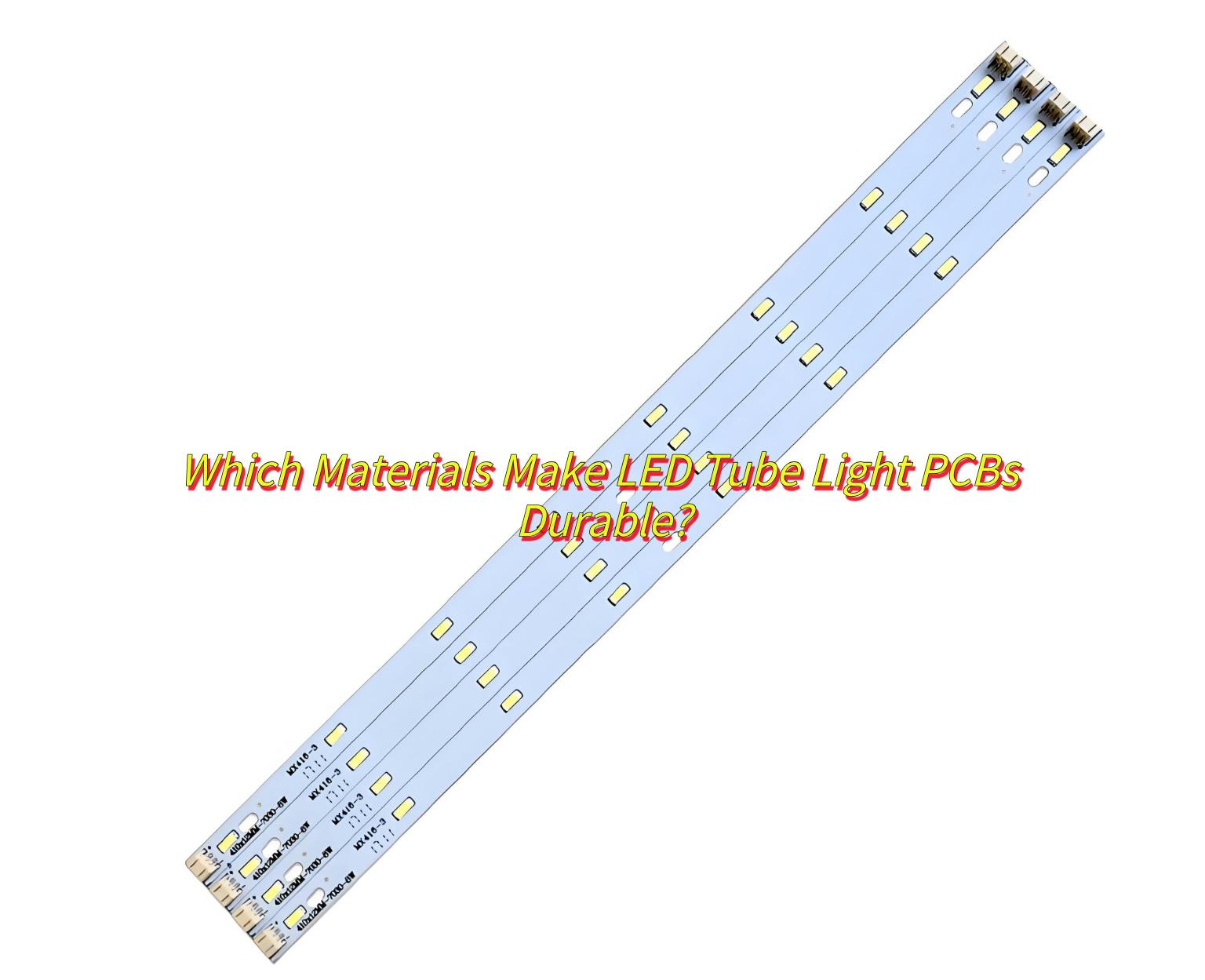
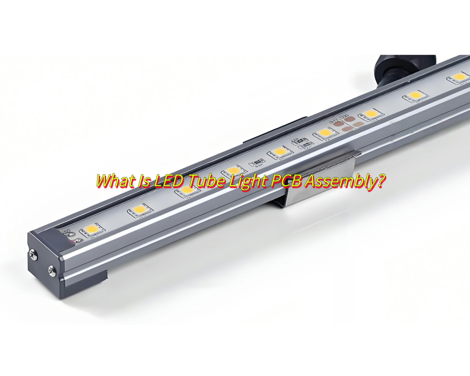
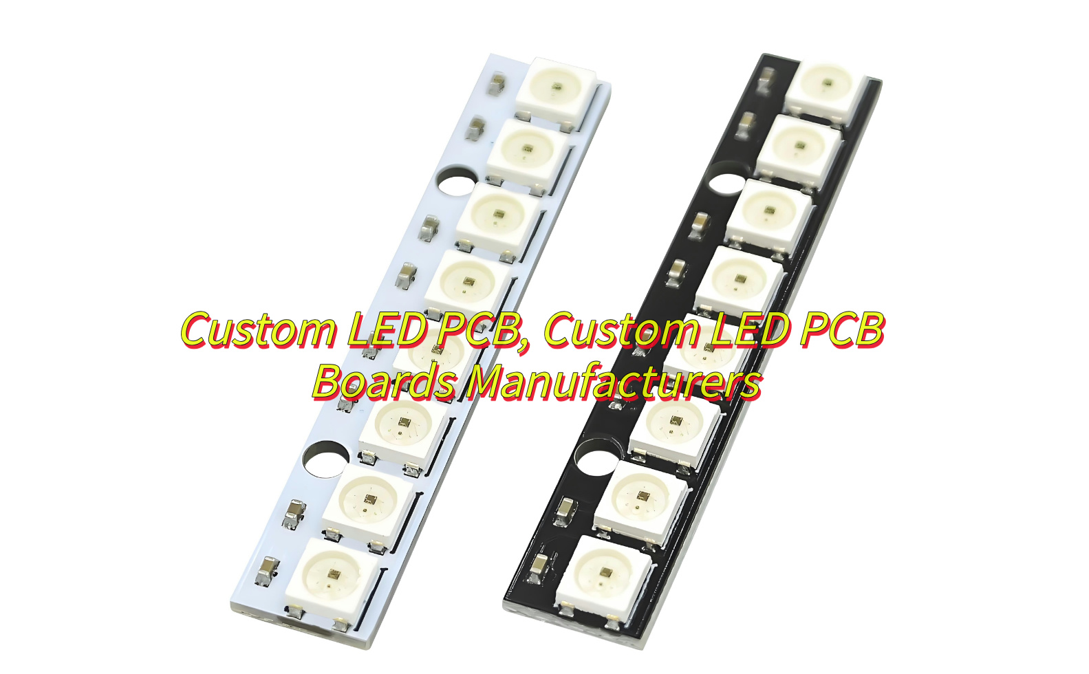
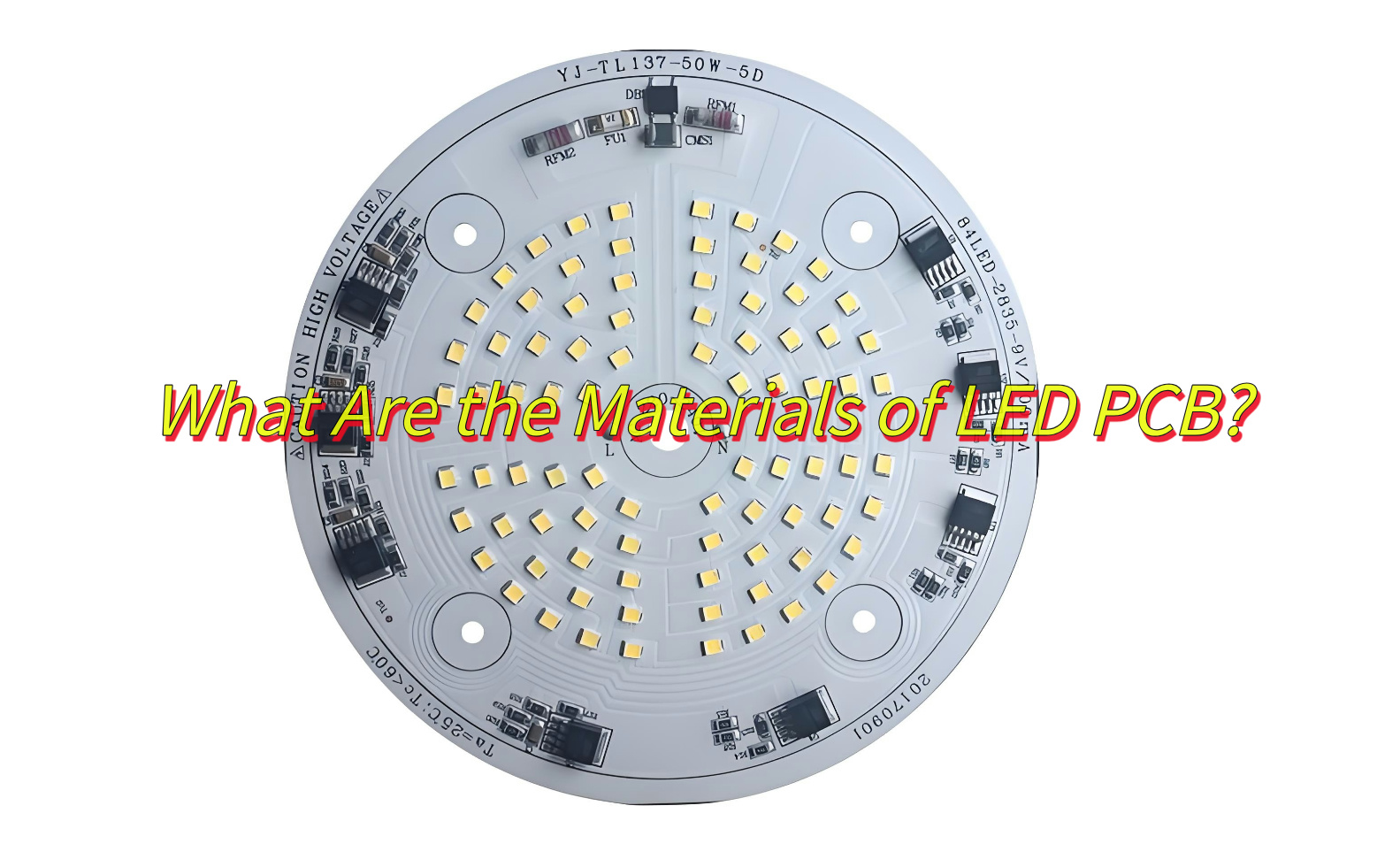
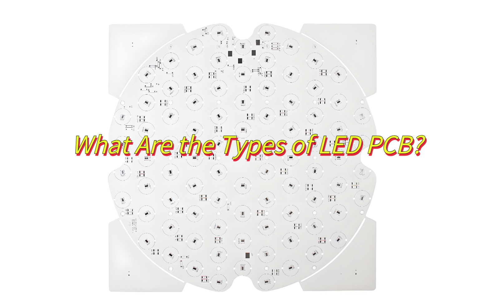
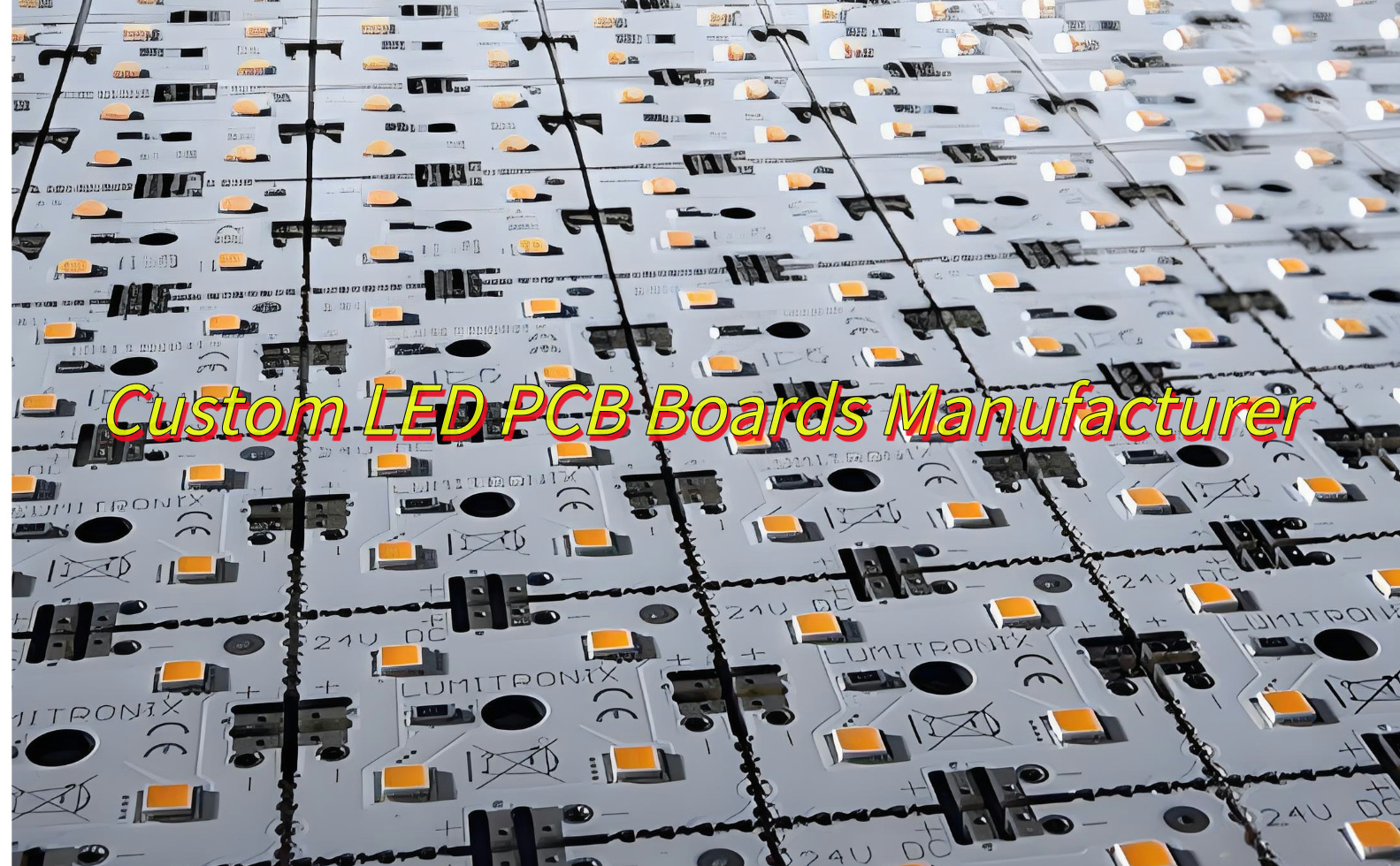
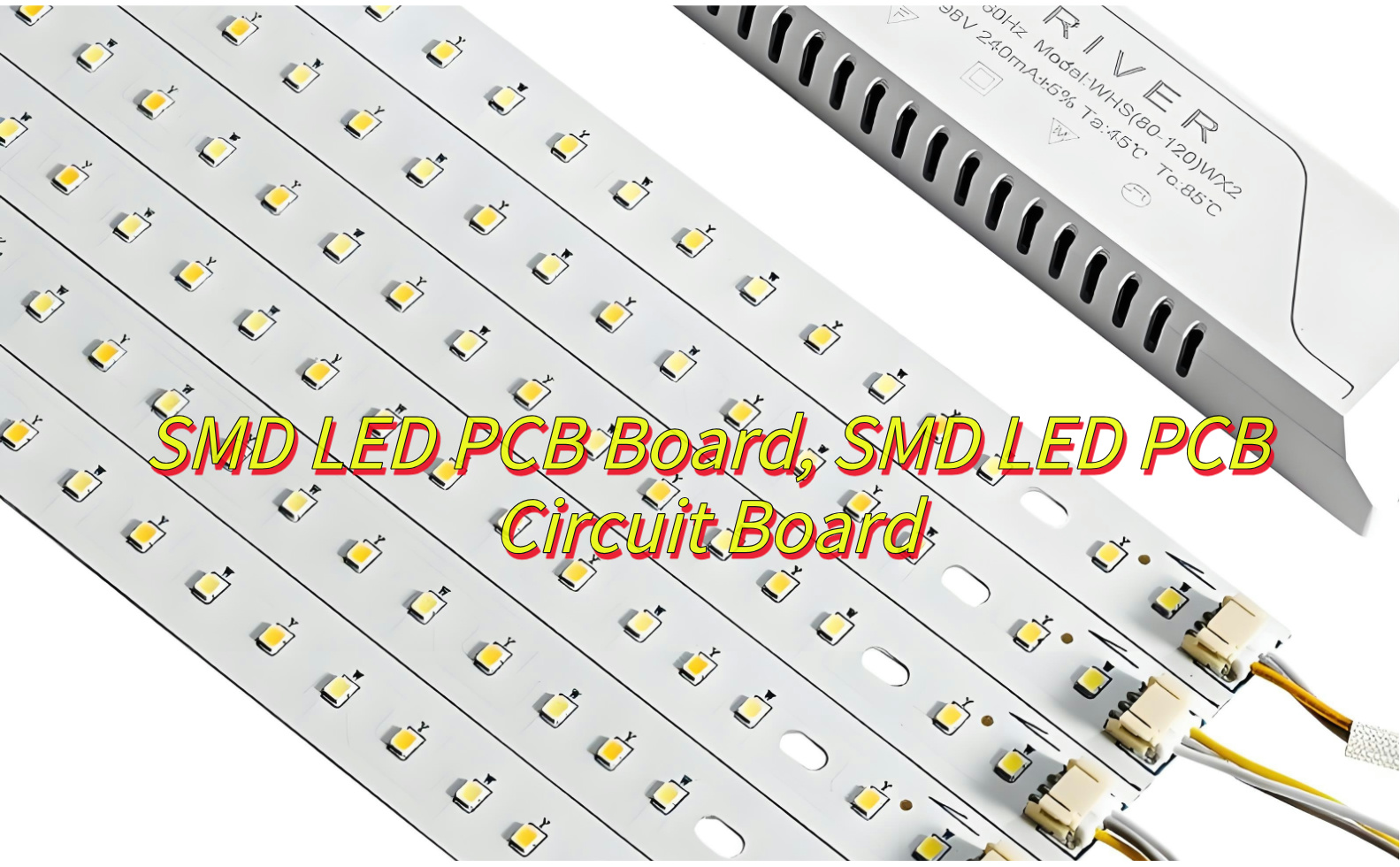
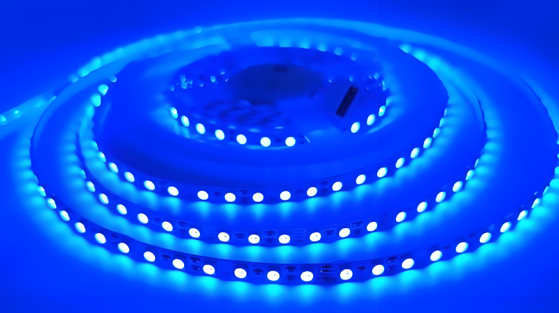
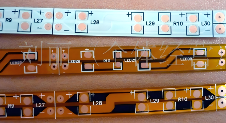
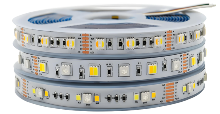
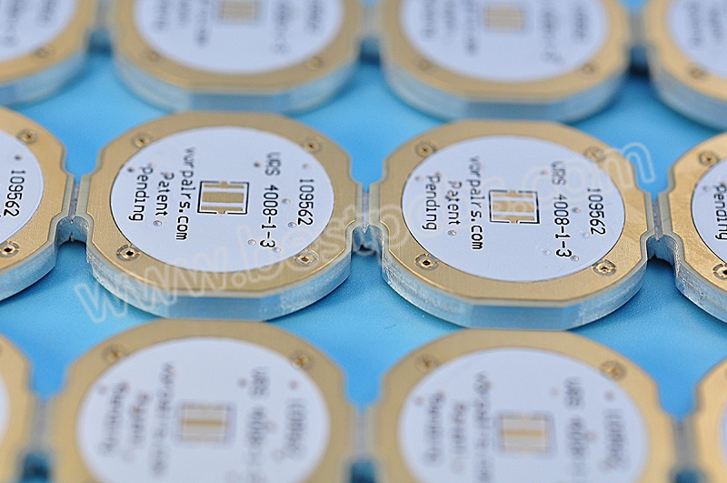
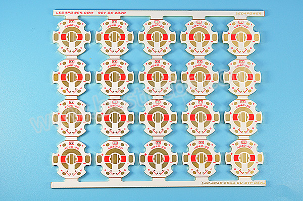
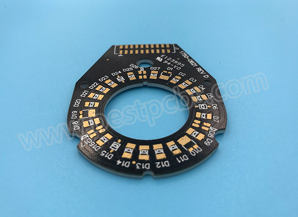
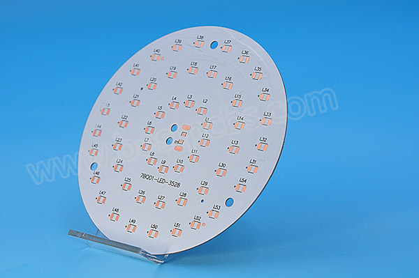
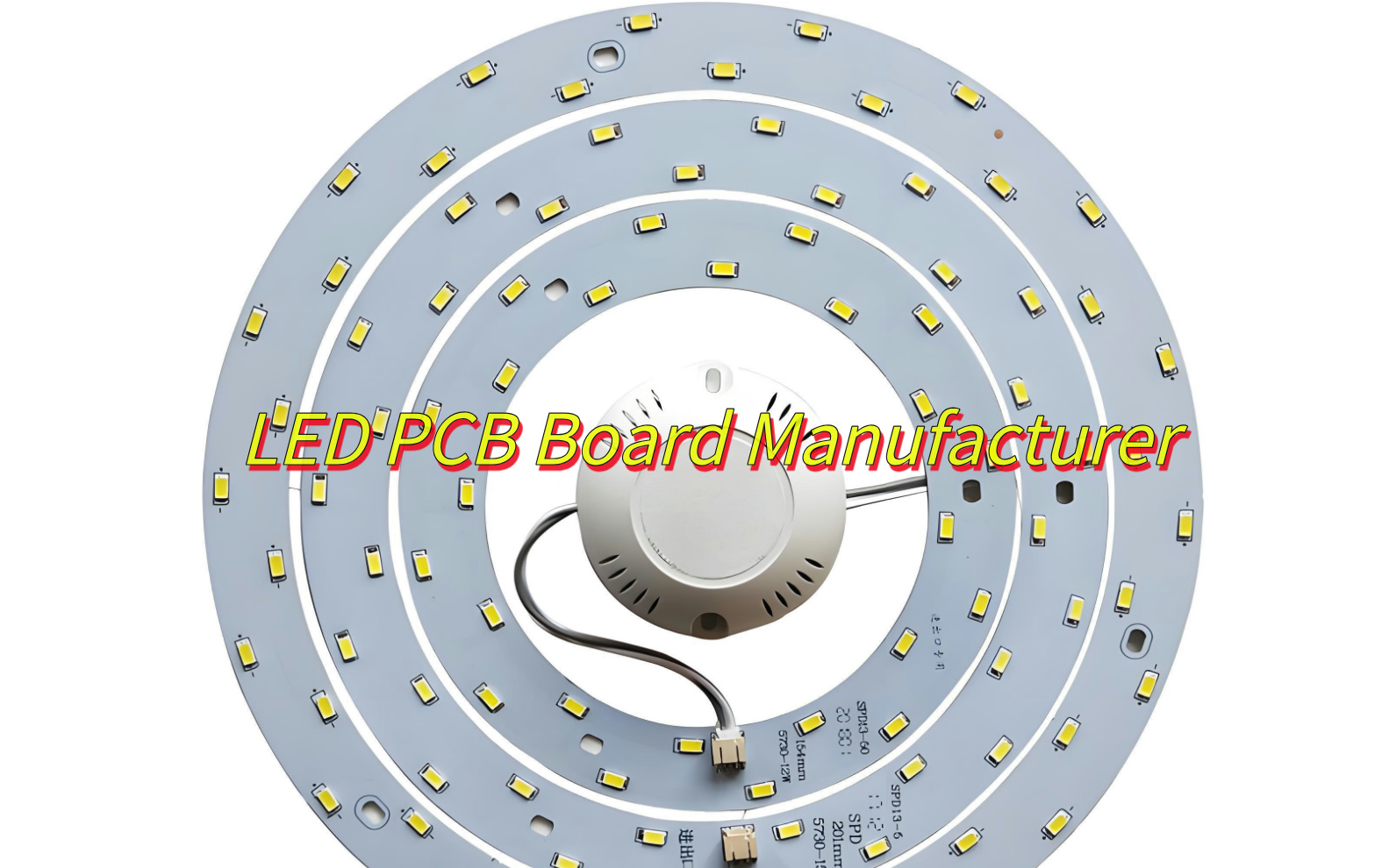
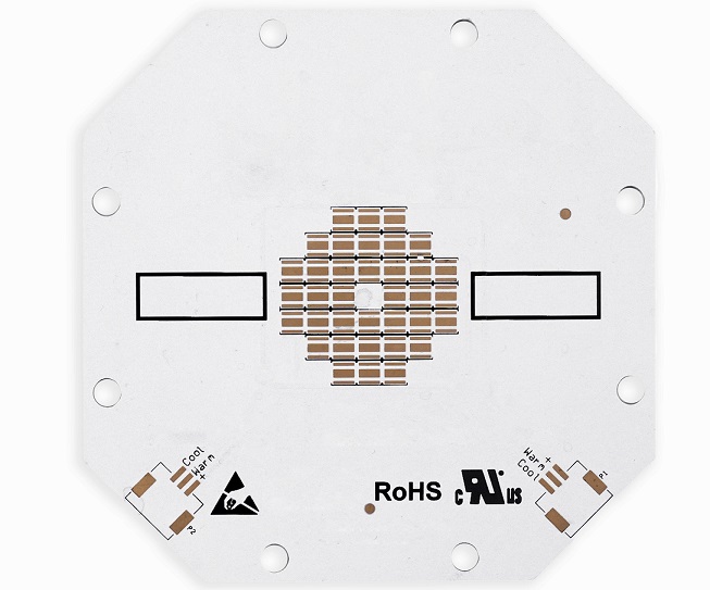
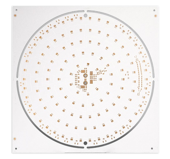
HASL Lead Free 94V0 LED PCB Product Photos
HASL Lead Free 94V0 LED PCB Specifications
| Product Name | HASL Lead Free 94V0 LED PCB |
| Base Material | Aluminum |
| Layer Count | 1L (Single Sided) |
| Board Thickness | 1.6mm +/-10% |
| Dielectric Thermal Conductivity | 1W |
| Copper Thickness | 1OZ |
| Solder Mask | White |
| Silkscreen | Black |
| Surface Finishing | HASL Lead-Free |
| Hole Tolerance | PTH: ±0.075; NTPH: ±0.05 |
| Testing | Testing Jig |
| Assembly | YES |
| Shape | Round |
Features of HASL Lead Free 94V0 LED PCB
- Lead-Free Soldering Process: HASL Lead-Free uses a soldering process that does not involve lead. It means this kind of PCB is safer for the environment and human health, especially in applications like LED lighting, where ROHS environmental compliance is important.
- Flame Retardant (94V-0): The 94V0 rating is one of the highest in terms of flame resistance and thermal stability. If a PCB has 94V-0 remarks, it means its PCB material can withstand high temperatures without catching fire. Because LED devices always generate much heat, it essential to use 94V-0 PCB to ensure the safety.
- Good Solderability: The surface finish provided by HASL offers an excellent soldering surface, it offers a reliable connection for LED components, minimizing the risk of poor solder joints that could lead to failure.
- Cost-Effective: The HASL process is one of the most cost-effective PCB finishes available. It offers an excellent balance between affordability and reliability, especially for high-volume production runs.
- Durability: The HASL Lead-Free 94V0 PCB is durable and resistant to wear and tear, it performs well even under demanding conditions, such as prolonged exposure to high temperatures and physical stress.
Advantages of Lead-Free HASL LED PCB
- The most significant advantage of lead-free HASL PCBs is that they are RoHS-compliant, meaning they do not contain any hazardous materials like lead.
- These PCBs can withstand and manage the heat generated by LEDs, thanks to the 94V0 flame retardant material. Combined with aluminum base, it offers better heat dissipation and reduce the risks of overheating in the high-power applications.
- The HASL process is less expensive compared to other surface finishes like ENIG, so it is a cost-effective solution for LED PCB manufacturing, especially in high-volume production.
- The uniformity of the soldering surface reduces the risk of defects and improves the overall performance of the LED circuit.
- The combination of a lead-free process and 94V0 flame-retardant rating means these PCBs are less likely to degrade over time due to high temperatures.
Lead-Free HASL vs ENIG LED PCB
The HASL process involves coating the PCB with a thin layer of solder, which is then leveled with hot air. Its full process is Clean PCB -> Micro-etch -> Apply high temperature flux -> Coated with tin -> Hot air smoothing -> Water washing. In the case of Lead-Free HASL, the solder used is free of lead, typically made of a combination of tin, silver, and copper. The result is a smooth, solderable surface, which is ideal for most standard PCB applications.
Pros:
- More affordable for high-volume production.
- Adequate for most standard LED applications.
- Environmentally friendly due to the lead-free process.
- Provides good solderability.
Cons:
- The surface finish is not as flat as ENIG, which can pose challenges for fine-pitch components or high-density boards.
- Less resistant to oxidation compared to ENIG.
Choose Lead-Free HASL if:
- You are looking for a cost-effective solution for standard LED applications.
- The operating environment is not excessively harsh.
- You are working with larger components or moderate-density designs.
- The application does not require extreme durability or long-term reliability.
In the ENIG process, a layer of nickel is first electroplated on the surface of copper then followed by immersion gold plating. The nickel acts as a barrier layer and the adhesion layer of gold, preventing oxidation and corrosion. And the gold layer provides good electrical conductivity and corrosion resistance, ensures a smooth and corrosion-resistant finish. ENIG provides a much flatter surface than HASL, which is ideal for fine-pitch components and high-density designs.
Pros:
- Extremely flat and smooth surface, ideal for fine-pitch and high-density boards.
- Superior corrosion resistance.
- Longer shelf life and better performance for high-end applications.
Cons:
- More expensive than HASL.
- Requires more complex manufacturing processes.
Choose ENIG if:
- You need premium performance for high-end applications.
- Your design involves fine-pitch components or high-density circuits.
- The LED application is exposed to harsh environments or requires long-term performance.
- Corrosion resistance and soldering reliability are critical for the application.
If you want to know more details betwen HASL and ENIG, view our another blog of HASL Lead Free vs ENIG: Understanding Their Differences.
Applications of Lead-Free HASL 94V0 LED PCB
- General LED Lighting – Used in residential, commercial, and industrial lighting applications.
- Automotive LED Lighting – use in automotive applications, such as headlights, indicator lights, and interior lighting.
- Outdoor Display Panels – Large LED displays, including billboards, outdoor signage, and digital screens.
- Consumer Electronics – In smart home devices, televisions, monitors, and portable electronics.
- Medical Equipment – Indicators, displays, or light sources.
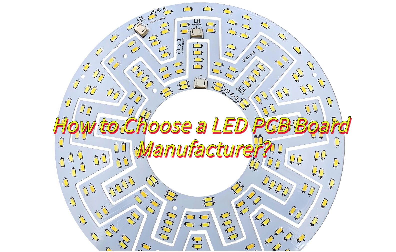
Detail LED PCB Manufacturing Capabilities
| Items | Capabilities |
| Base Material | Aluminum / Copper / Stainless steel |
| Base Material Thickness (exclude CU) | 0.30mm / 0.40mm / 0.50mm / 0.60mm/ 0.80mm /1.0 mm/ 1.2 mm / 1.6mm / 2.0 mm / 2.4mm / 3.0mm |
| Thermal Conductivity | 1W / 1.5W / 2.0W / 3.0W |
| Solder Mask Color Option | White, Black, Green, Blue, Yellow, Red |
| Layer | 1-10 layers |
| Max Board Dimension | 24*64″(610*1625mm) |
| Min Board Thickness | 0.6mm |
| Max Board Thickness | 4.0mm |
| Conductor Thickness | 0.5oz-10oz |
| Min Line Width/Space | 4/4mil (0.10/0.10mm) |
| Tg Value | 130 / 150 |
| Min Solder Mask Bridge | 8mil (0.20mm) |
| Min Hole Diameter | 10mil (0.25mm) |
| Min Punch Hole Dia | 0.12″ (3.0mm) |
| Min Hole Spacing | 16mil (0.4mm) |
| Min PAD Ring (Single) | 3mil (0.075mm) |
| PTH Wall Thickness | Normal: 0.59mil (15um); HDI: 0.48mil (12um) |
| Min Solder PAD Dia | 14mil (0.35mm) |
| Min BAG PAD Margin | 5mil (0.125mm) |
| PTH/NPTH Dia Tolerance | PTH: ±3 mil (0.075mm); NPTH: ±2mil (0.05mm) |
| Hole Position Deviation | ±3mil (0.075mm) |
| Outline Tolerance | CNC: ±6 mil (0.15mm); Die Punch: ±6 mil (0.1mm) |
| Max Aspect Ratio | 10:1 |
| Surface Treatment | ENIG, ENEPIG, OSP, HASL (LF) |
| Halogen Free | Yes(optional) |
| ROHS | Yes |
| Flammability | 94V-0 |
| Dielectric Strength | >1.5Kv (L/S >1.5mm); >3.0Kv (L/S >3.0mm) |
| Wrap & Twist | ≤ 0.75% |
| Thermal Stress | 3 x 10 Sec @ 280 ℃ |
LED PCB Prototype Lead Time
| Prototype(<1m²) | Layers | Normal Service | Expedited Service |
| LED PCB | 1 Layer | 1 – 1.5 weeks | 48 hours |
| 2 Layers | 2.5 – 3 weeks | 168 hours | |
| 4 Layers | 3 – 4 weeks | 1.5 weeks | |
| 6 Layers | 4 – 5 weeks | 2 weeks | |
| 8 Layers | 5 – 6 weeks | TBD | |
| 10 Layers | 6 – 7 weeks | TBD |
LED PCB Mass Production Lead Time
| Mass Production | Layers | Normal Service | Expedited Service |
| LED PCB | 1 Layer | 2 – 2.5 weeks | 1 week |
| 2 Layers | 3 – 4 weeks | 1.5 – 2 weeks | |
| 4 Layers | 4 – 5 weeks | 2 weeks | |
| 6 Layers | 5 – 6 weeks | 2.5 weeks | |
| 8 Layers | 6 – 7 weeks | 3 – 4 weeks | |
| 10 Layers | 7 – 8 weeks | TBD |
Package Method
- Standard Packaging: PCBs are carefully packed in anti-static bags or ESD-safe boxes with vacuum to prevent damage during shipping, and outer standard carton box packing.
- Custom Packaging: We also offer custom packaging based on customer specifications to suit unique shipping or storage requirements.
Payment & Shipping Terms
- Payment Terms: We accept major payment methods, including T/T (Telegraphic Transfer), PayPal, and L/C (Letter of Credit) for large orders.
- Shipping Terms: We offer various shipping methods including express (DHL, FedEx, UPS), air, and sea freight depending on urgency and order size.
- Incoterms: EXW, FOB, CIF, DDP, DDU, as per customer preference.
- Lead Time for Shipping: Typically 4-6 days for express and 15-30 days for sea freight, depending on the destination.
For more information about OEM ODM HASL lead free 94v-0 LED PCB, welcome to contact us at any time.