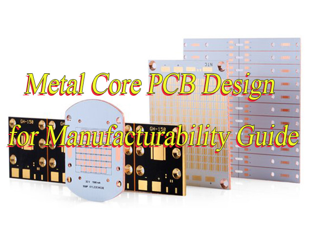
Looking for PCB manufacturing companies in UAE? This blog is mainly about list, selection guide, PCB types of PCB manufacturing companies in UAE.
PCB Manufacturing Companies in UAE are gaining attention due to local demand for electronics, automation, energy control modules, power conversion units, and security systems. PCB Manufacturing Companies in UAE also attract engineers who prefer short supply routes and fast communication. This article explains how the UAE market works, which suppliers are active, and how buyers can compare strengths before placing orders.
List of PCB Manufacturing Companies in UAE
1. PCB Power Market
- Main Business: Quick-turn PCB fabrication, prototype builds, and small-batch manufacturing.
- Advantages: Stable quality for low-layer FR4 boards, simple quote process, and friendly service for students and hobbyists.
- Production Capability: 1–8 layers, standard TG materials, HASL/ENIG finishes, basic impedance builds.
- Lead Time: 5–12 working days for standard orders, with express service available.
2. EMatrix Electronics
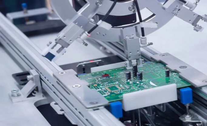
- Main Business: PCB manufacturing, PCB assembly, component sourcing, box-build, and embedded system support.
- Advantages: Local engineering communication, on-site support, and guidance for PCB redesign when needed.
- Production Capability: 2–10 layers, FR4, high-TG, ENIG, HASL, stencil production, and small SMT runs.
- Lead Time: 7–14 working days depending on the part count and assembly density.
3. Al Taj
- Main Business: Custom PCB fabrication, cable assembly, wiring harness production, and industrial electronics assembly.
- Advantages: Good for mixed projects that require both board manufacturing and custom wiring.
- Production Capability: 2–6 layers, FR4 boards, basic SMT assembly, through-hole assembly, and cable-board integration.
- Lead Time: 10–18 days depending on project size.
4. GREAT Waters
- Main Business: PCB prototyping, PCB assembly, reverse-engineering, firmware programming, and repair services.
- Advantages: Suitable for maintenance teams and companies upgrading older devices.
- Production Capability: 1–6 layers, rework, redesign, simple RF routing, and mixed-technology assembly.
- Lead Time: 8–15 days for PCB builds and assembly.
5. Atlantis Engineering
- Main Business: Custom electronics development, PCB fabrication, firmware, IoT product support, and prototype assembly.
- Advantages: Good for early-stage product design, enclosure design, and complete device planning.
- Production Capability: 2–6 layers, low-run PCB assembly, IoT module integration, and EMC-aware redesign.
- Lead Time: 12–20 working days.
6. Fastron Group Partners
- Main Business: PCB manufacturing from international production lines, plus stocking of RF inductors and passive components.
- Advantages: Good component availability for RF boards, radio modules, and mixed-signal circuits.
- Production Capability: 2–12 layers, controlled impedance, ENIG finishes, and RF materials on request.
- Lead Time: 12–20 days based on factory load.
7. Al Mashriq Electronics
- Main Business: PCB design, PCB manufacturing coordination, on-site testing, and EMC trouble-shooting.
- Advantages: Strong design support and hands-on debugging for local users.
- Production Capability: 2–6 layers, stencil support, DIP assembly, and bench-level testing.
- Lead Time: 10–16 working days.
How to Select PCB Manufacturing Companies in UAE?
A detailed selection guide to PCB manufacturing companies in UAE:
1. Prioritize Certification Compliance
- ECAS Mandatory Certification: All PCBs exported to the UAE must pass ECAS certification from the Emirates Authority for Standardization and Metrology (ESMA), covering safety, electromagnetic compatibility, energy efficiency, and other standards. Technical documents, circuit diagrams, PCB layout drawings, and test reports from local certified laboratories (such as IEC 60335 and CISPR standards) must be provided in Arabic.
- MPCI Declaration System: As of July 2025, all shipments must submit container data to the UAE National Advance Information Center (NAIC) in advance, including bill of lading numbers, HS codes, and cargo values. The grace period extends until March 2026, with fines for non-compliance.
- Localization Requirements: Non-UAE companies must appoint a local agent or authorized representative and ensure product labels include Arabic information (such as model numbers, electrical parameters, and manufacturer addresses).
2. Match Technical Capabilities
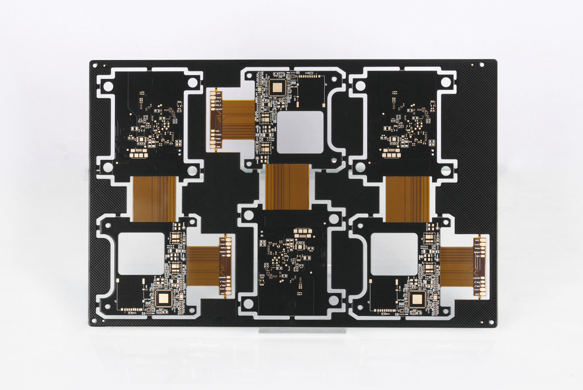
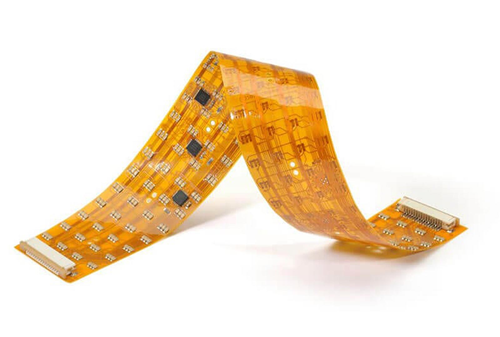
- Advanced Technical Support: Prioritize manufacturers with capabilities in HDI (High-Density Interconnect), FPC (Flexible Printed Circuit), rigid-flex boards, and package substrates (such as ABF carriers) to meet high-precision requirements for 5G, AI servers, and new energy vehicles.
- Process Control Standards: Focus on hard indicators such as solder joint penetration rate (≥75%), insulation resistance (>1000MΩ), and dimensional tolerance (±0.5mm), as well as reliability verification through thermal cycling tests (-40°C to 125°C, 1000 cycles) and salt spray tests.
- Environmental Material Application: Use halogen-free substrates (compliant with IEC 61249-2-21), bio-based resins, and biodegradable materials, certified under RoHS and REACH, to reduce hazardous substances like lead and cadmium.
3. Manage Cost and Lead Time
- Price Transparency: Bulk orders are typically priced per solder joint (3-5 RMB/PINS), with sample prototyping fees starting at approximately 50 RMB. Complex designs require additional quotes. Compare bulk discounts and rush fee policies (such as JLCPCB’s 12-hour/24-hour expedited services).
- Lead Time Guarantee: Confirm production cycles (e.g., 12-72 hours for samples, with clear cut-off times and production scheduling rules for bulk orders) and consider logistics time (sea freight approximately 30 days, air freight 3-5 days) to avoid delays impacting project timelines.
- Supply Chain Resilience: Evaluate manufacturers’ raw material procurement channels (e.g., copper foil, resin), inventory management capabilities, and capacity adjustment flexibility to respond to sudden demand changes.
4. Quality Control Systems
- Incoming Material Inspection: Conduct pre-warehouse inspections of PCB substrates (FR-4, high-frequency materials) and components for appearance and electrical performance to prevent defective items from entering the production line.
- Process Monitoring: Implement XRF screening for hazardous substances, ICP-MS for precise limit detection, solder joint AOI (Automated Optical Inspection), and ICT (In-Circuit Test) to ensure soldering quality and electrical performance.
- Final Product Verification: Perform insulation resistance tests, voltage withstand tests, functional tests (simulating actual operating conditions), and environmental adaptability tests (high-low temperature aging, vibration, and impact tests).
5. Localized Service Support
- Language and Communication: Ensure technical teams provide bilingual (English/Arabic) communication to promptly respond to design changes and technical inquiries.
- After-Sales Guarantee: Establish a quality issue feedback mechanism, offering quick repair, replacement, and return services, and support on-site factory audits for clients (some high-risk products require factory inspections).
- Market Insights Monitor: UAE industrial policies (such as Dubai Free Zone tax incentives), industry trends (such as growing demand for 5G base stations and electric vehicle BMS), and select partners with local market experience.
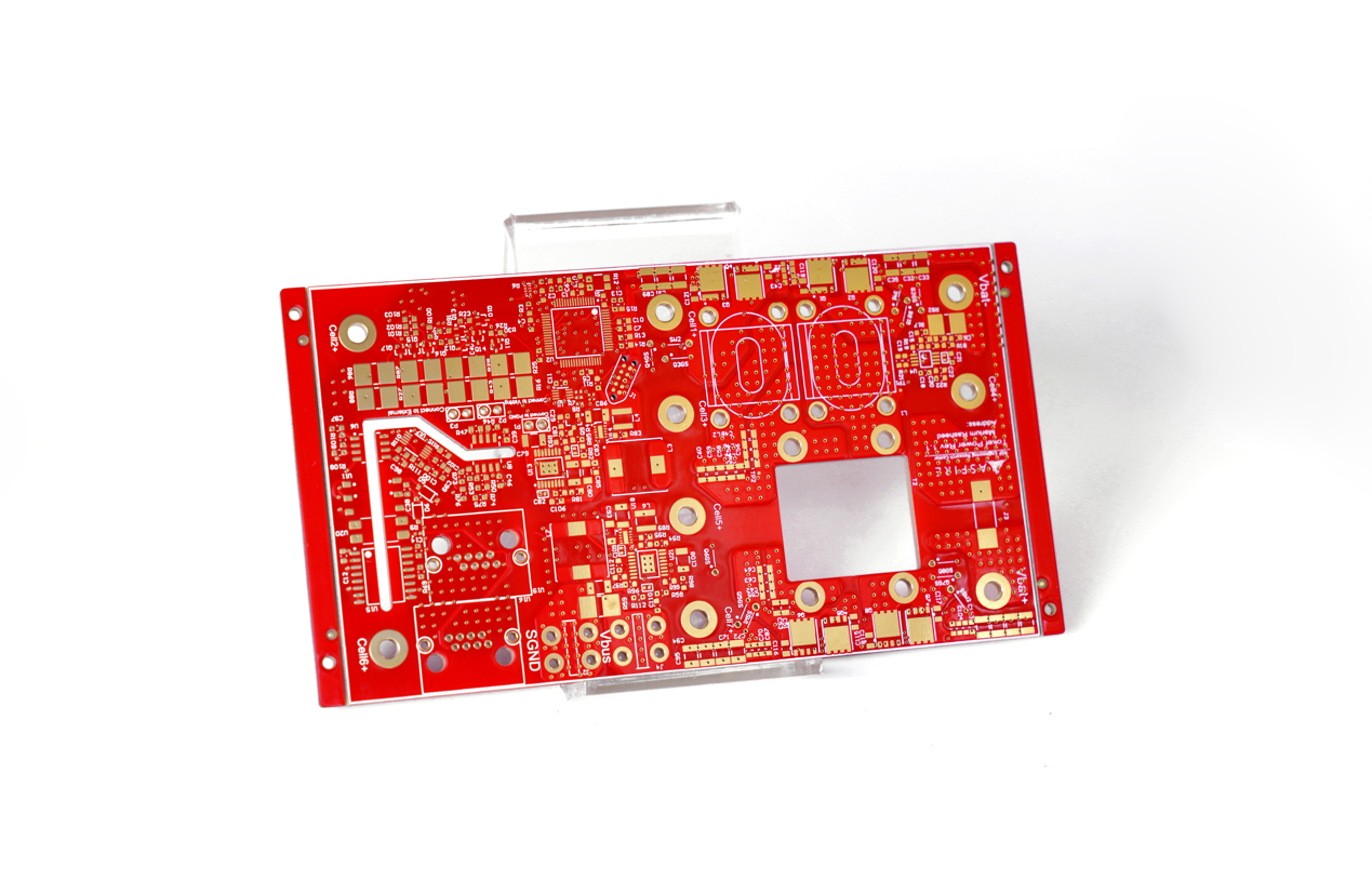
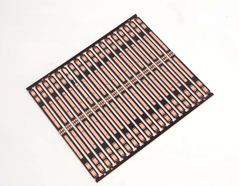
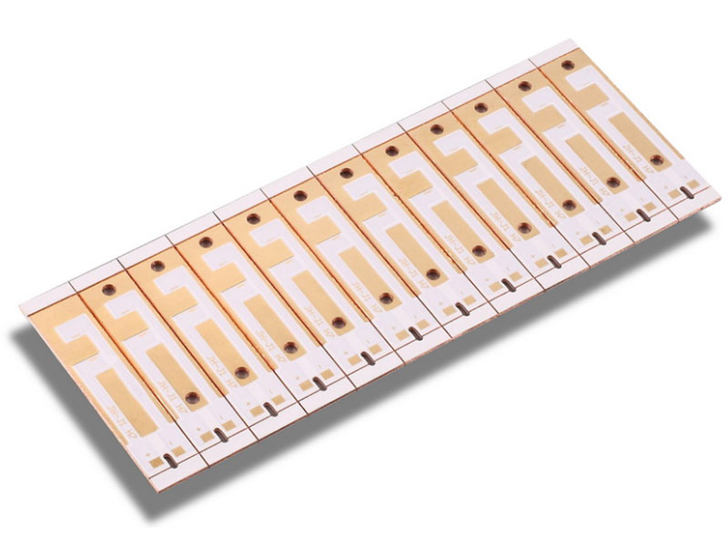
PCB Types Offered by PCB Manufacturing Companies in UAE
PCB Types Offered By UAE PCB Manufacturing Companies:
- Single-layer PCBs: Used for lighting products, basic power supplies, and simple sensors.
- Double-layer PCBs: Suitable for control panels, audio devices, and security modules.
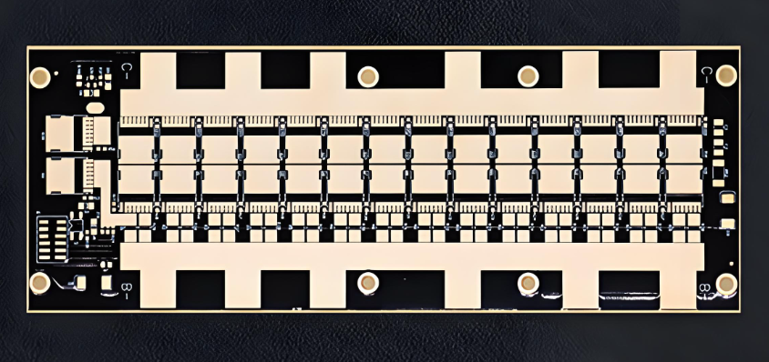
- Multilayer PCBs (4–10 layers): Common in telecom systems, industrial automation, and embedded modules.
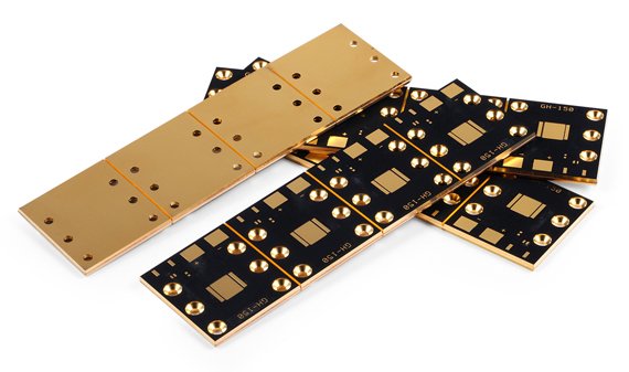
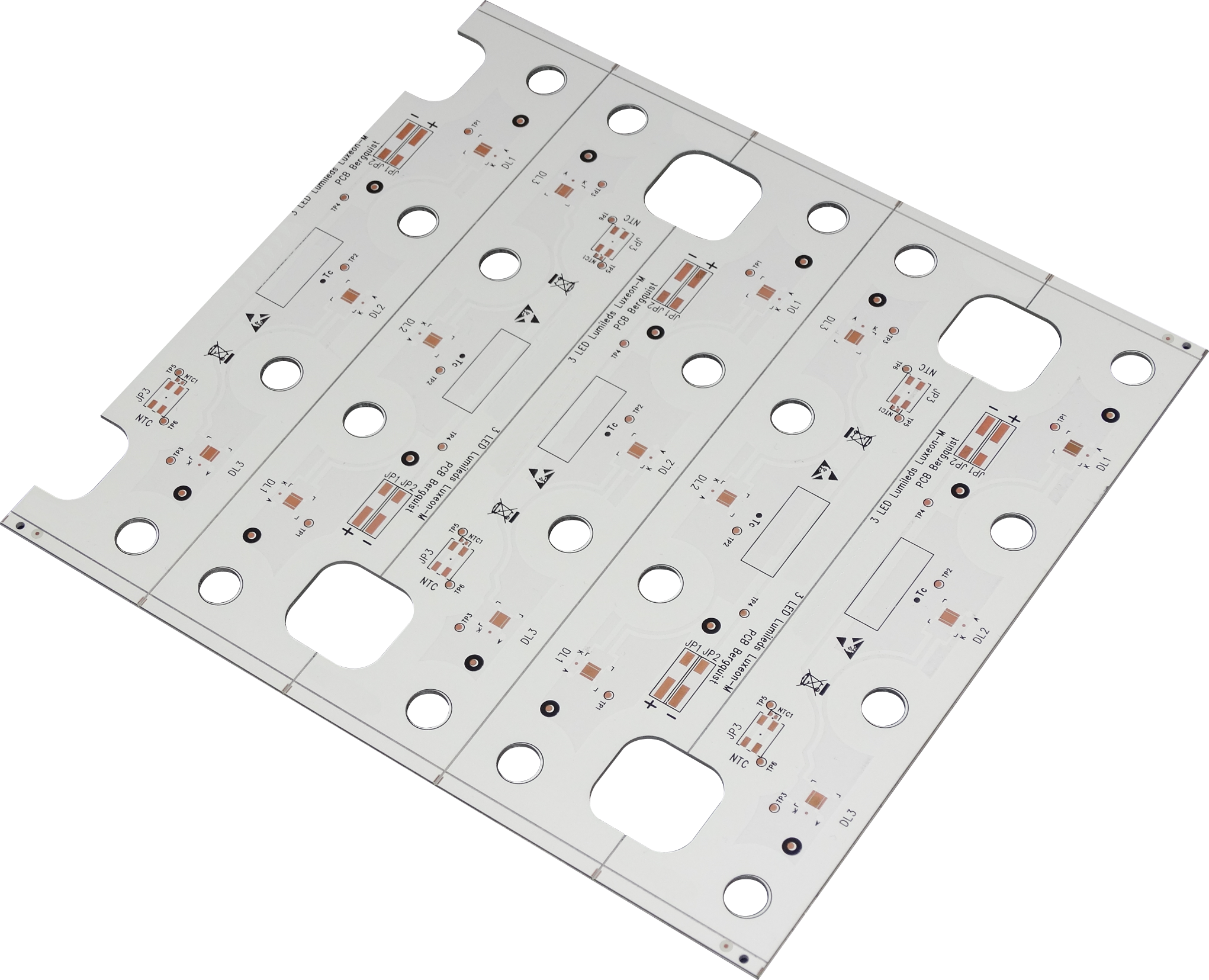
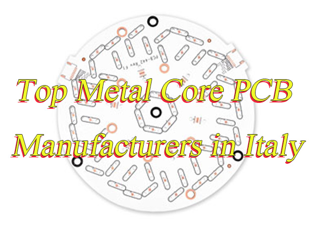
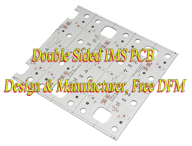
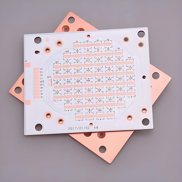
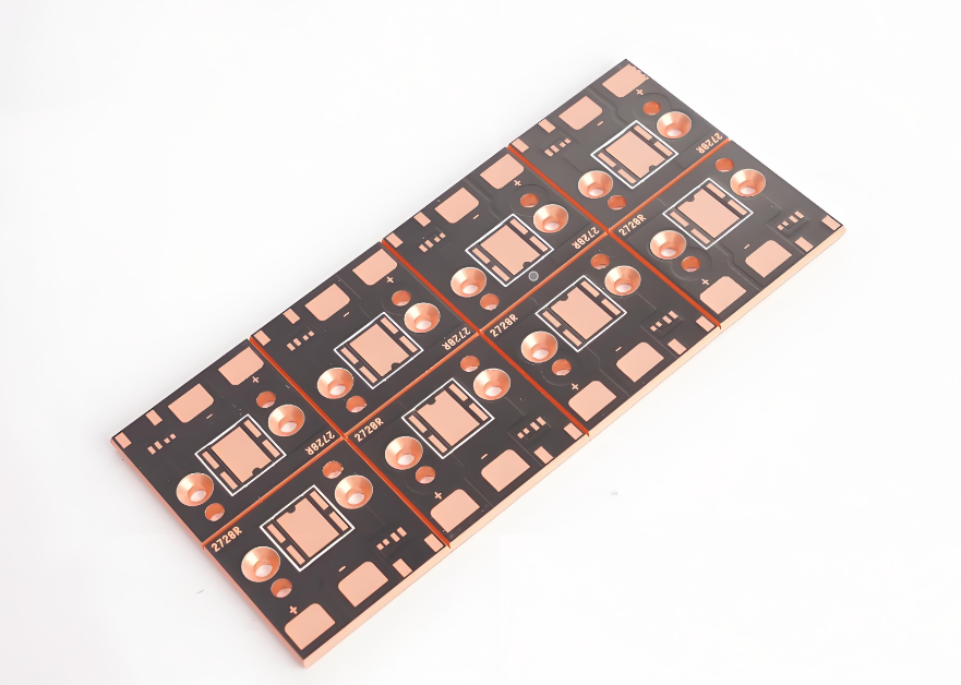
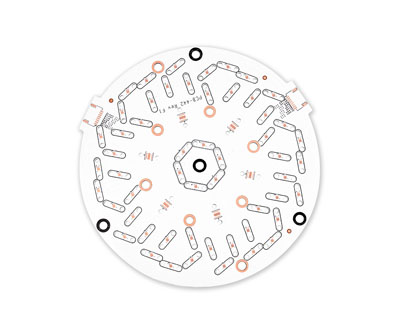
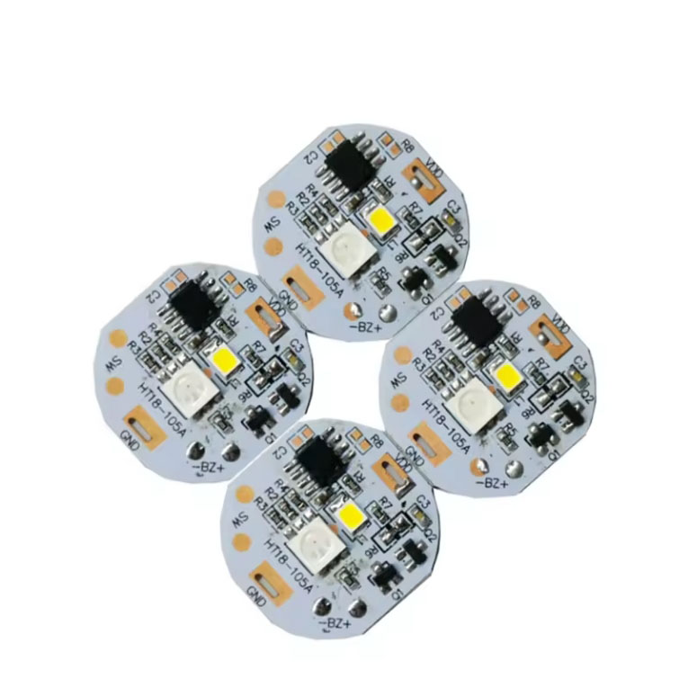
- Aluminum PCBs: Often used for LED lighting and power circuits requiring heat control.
- High-TG PCBs: Applied in automotive electronics and energy equipment.
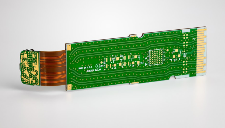
- Rigid-flex PCBs: Sometimes available through UAE design houses but fabricated offshore.
- RF PCBs: Usually sourced from global suppliers, as local plants have limited capability.

Delivery Delays: China-UAE DDP Direct Shipping
Many UAE buyers experience long delivery times when working with suppliers who depend on slow freight channels or inconsistent shipping agents. These delays disrupt testing schedules and affect assembly timelines. Some factories also provide unclear transit updates, leaving customers unsure about the actual arrival date of their order. The result is more waiting, higher internal pressure, and frequent production rescheduling.
However, EBest Circuit (Best Technology) solves this with stable China–UAE DDP direct shipping. Our dedicated logistics channels shorten transit time and provide predictable delivery for both prototypes and mass production. We also handle customs clearance, duty processing, and local import steps, so customers avoid paperwork and hidden administrative tasks. Even better, our team tracks every shipment and updates clients throughout the journey. This ensures that UAE engineers can plan assembly work with confidence and move projects forward without disruptions.
PCB Quality Defects: Free DFM Audits Before Production
Some PCB manufacturers accept customer files without proper review. This leads to hidden design issues such as incorrect drill spacing, thin copper near vias, or solder mask misalignment. These problems often appear only after fabrication, resulting in failed tests, extra costs, and repeated revisions. UAE customers report that this situation causes major delays in new product development.
EBest Circuit (Best Technology) avoids these issues by providing free DFM audits before production. Our engineering team reviews Gerber files, stack-ups, drill charts, impedance needs before any board enters the line. This early check catches potential defects and gives customers practical suggestions to improve reliability. We also apply strict AOI, electrical testing, and controlled impedance checks to ensure that every board meets the expected standard. With this approach, UAE customers enjoy stable quality, fewer surprises, and smoother product launches.
Slow After-Sales Support: Technical Team 48H Online Response
When buying from some PCB manufacturers, clients often wait several days for technical support. This slow feedback becomes a serious obstacle during debugging, layout revisions, or NPI trials. Some suppliers only provide basic answers, which does not help engineers solve complex PCB or assembly issues. These delays extend development cycles and hurt time-to-market plans.
EBest Circuit (Best Technology) improves this experience with a technical team that responds within 48 hours. Our engineers cover CAM analysis, fabrication processes, SMT optimization, impedance guidance, and stack-up planning. UAE buyers receive clear explanations instead of generic comments. We also support PCBA troubleshooting with layout reviews, component alignment checks, and process suggestions. This fast and professional assistance helps customers maintain their project timeline and resolve issues quickly. It also builds stronger technical confidence throughout the production cycle.
Hidden Costs: All-Inclusive Pricing Without Extra Cost
Many PCB manufacturers offer attractive initial quotes but later add charges for tooling, testing, documentation, packaging, and even export handling. These hidden fees complicate budgeting and often result in higher-than-expected total cost. UAE procurement teams mention that this lack of transparency creates frustration and slows approval processes.
To avoid this, EBest Circuit (Best Technology) provides all-inclusive pricing with no unexpected fees. Our quotations cover material, drilling, plating, surface finishing, AOI, electrical test, and export documentation. For PCBA orders, we include SMT, DIP, testing, and component sourcing in a clear breakdown. Customers know the total cost from the start, which helps finance teams plan without uncertainty. This transparent pricing makes project management easier and helps buyers work more efficiently.
Case Studies of Our UAE PCB Manufacturing Project
Project Background
A UAE-based industrial equipment manufacturer required custom high-performance PCB components for new product development. Operating in a high-temperature Middle Eastern environment, the client demanded exceptional PCB durability and long-term stability, alongside rapid response capabilities for market launch needs.
Project Requirements
- Compliance with IPC-6012 Class 2 standards, ensuring stable electrical performance at 125°C continuous operating temperature. Vibration resistance must pass IEC 68-2-6 testing.
- Signal path impedance matching required 50±5Ω control, validated via Time-Domain Reflectometry (TDR).
- Sample delivery within 14 working days, accompanied by comprehensive DFM (Design for Manufacturing) analysis reports and reliability test data packages.
Solution
- Utilized FR-4 substrate with CTI ≥175 and thermosetting resin system to enhance high-temperature resistance. Vacuum lamination minimized interlayer voids, improving mechanical strength.
- Implemented parallel engineering across design, production, and testing phases: EDA software for signal integrity simulation, X-ray drilling alignment for precision, and dual AOI/flying probe systems for defect detection.
- Deployed digital production management for real-time process parameter monitoring and automatic deviation alerts to maintain stable process windows.
Result
- Samples passed client acceptance tests with 100% first-pass yield. Impedance deviations stayed within ±4.2Ω, and post-thermal aging electrical degradation remained below 2%, exceeding expectations.
- Bulk order delivery time reduced to 13 days, achieving 97.8% production yield with zero critical defects. Client recognized the project as “exceeding industry benchmarks.”
- Full digital quality traceability provided, including material batch records, process parameters, and test reports, enabling real-time remote verification by the client.
Why Choose EBest Circuit (Best Technology) for Global PCB Manufacturer?
Reasons why choose us for global PCB manufacturer:
- 19-Year Expertise: Leverages 19 years of industry experience with standardized process libraries and failure case databases to quickly identify design risks and provide proven solutions, reducing engineer trial costs.
- Certified Compliance: Holds ISO 9001, IATF 16949 automotive, ISO 13485 medical, and RoHS certifications to satisfy EU, Middle East, and other market access requirements while mitigating compliance risks.
- Competitive Pricing: Delivers cost-sensitive design solutions through material optimization and process innovation, reducing BOM costs by 15%-20% while meeting IPC-6012 standards, ideal for budget-sensitive consumer electronics projects.
- Rapid Prototyping: Enables 24-hour turnaround for urgent orders with TDR impedance validation and AOI inspection, accelerating prototype verification for designers and cutting product launch cycles by over 30%.
- 99.2% On-Time Delivery: Ensures 12-14 day standard lead times and 7-day express delivery for urgent orders via intelligent production scheduling and global supply chain coordination, meeting procurement stability demands.
- Batch Inspection Quality Control: Implements 100% inspection coverage during mass production with flying probe testing and reliability verification, maintaining over 98% yield rates for zero-defect assurance to engineers.
- Free DFM Analysis: Offers complimentary design-for-manufacturing reports during design phase, including signal integrity simulation, impedance matching recommendations, and solderability optimization to preempt production issues.
- Transparent Traceability: Maintains digital records of material batches, process parameters, and test data with unique ID tracking, enabling real-time quality verification for international procurement transparency needs.
Welcome to contact us to get a free quote if you have any request for PCB design, prototyping, mass production and assembly: sales@bestpcbs.com.