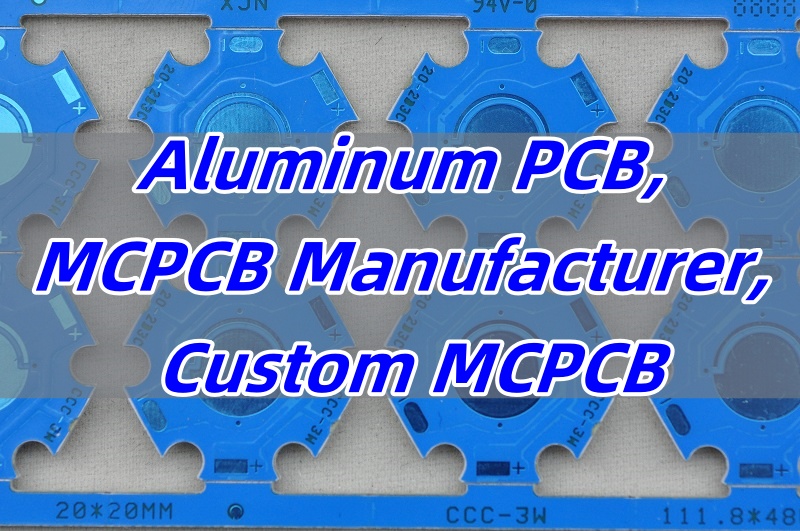
Seeking top bare LED PCB solutions? This guide dives into components, types, advantages and production while empowering you to evaluate manufacturers, ensure quality, and optimize costs from 8×8 matrices to LED bulbs.
Need a bare LED PCB partner that keeps pace with your deadlines? EBest Circuit (Best Technology) delivers 24-hour bare LED PCB rapid prototyping and 5-day mass production for urgent orders. We specialize in small-batch manufacturing (from 1 unit) with no hidden fees, ideal for startups and R&D projects. Our sales and engineering teams respond within 2 hours online, offering real-time design feedback and instant quotes. Advanced capabilities include multilayer boards (up to 20 layers), ENIG/HASL finishes, and ±0.03mm laser-drilled vias, ensuring precision for LED matrices and thermal-heavy designs. With 99.2% on-time delivery and ISO 9001-certified quality control, we guarantee reliability without compromising speed. Request a quote today and experience agile, cost-effective PCB solutions tailored to your timeline. Contact us now: sales@bestpcbs.com.
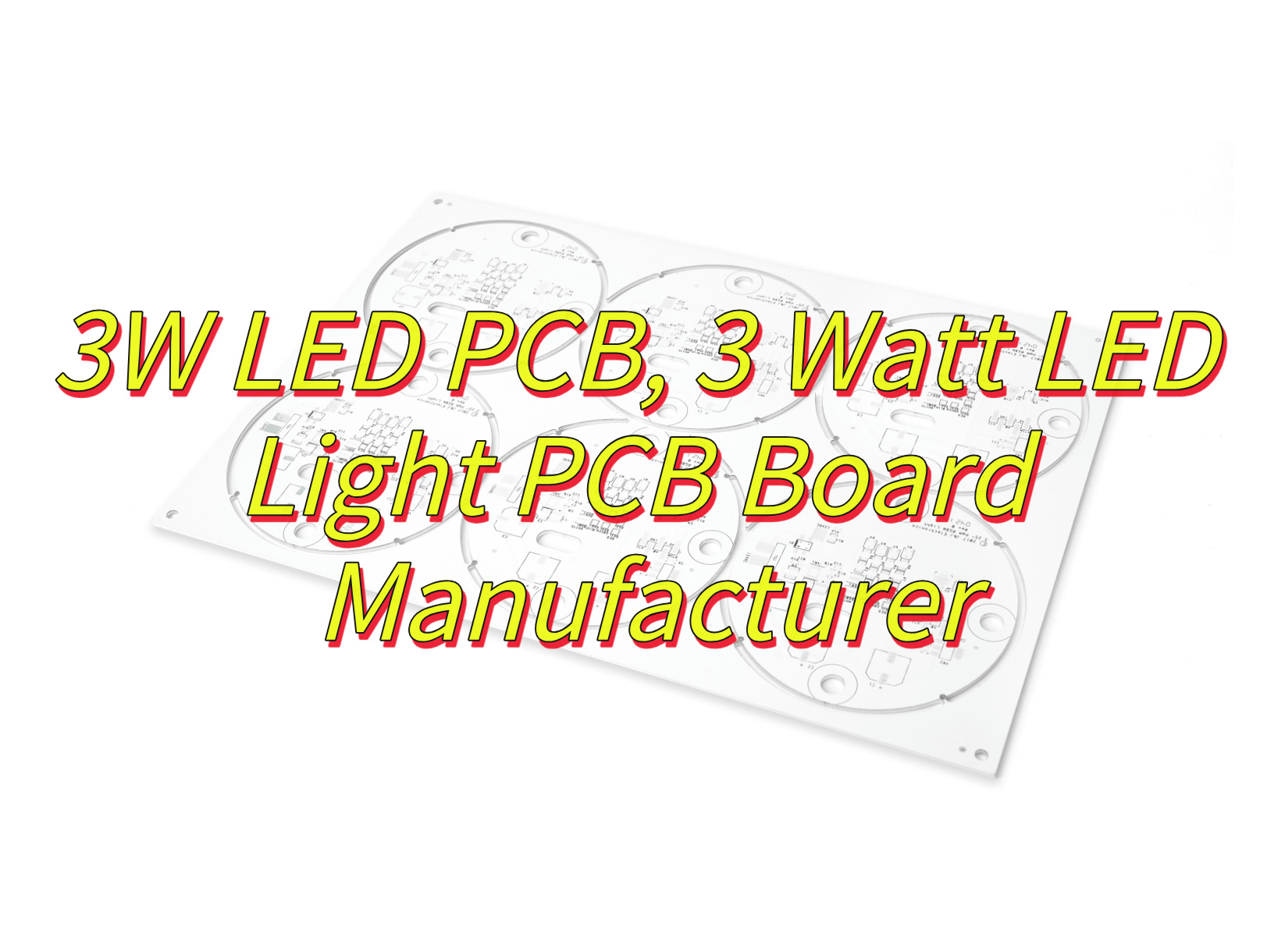
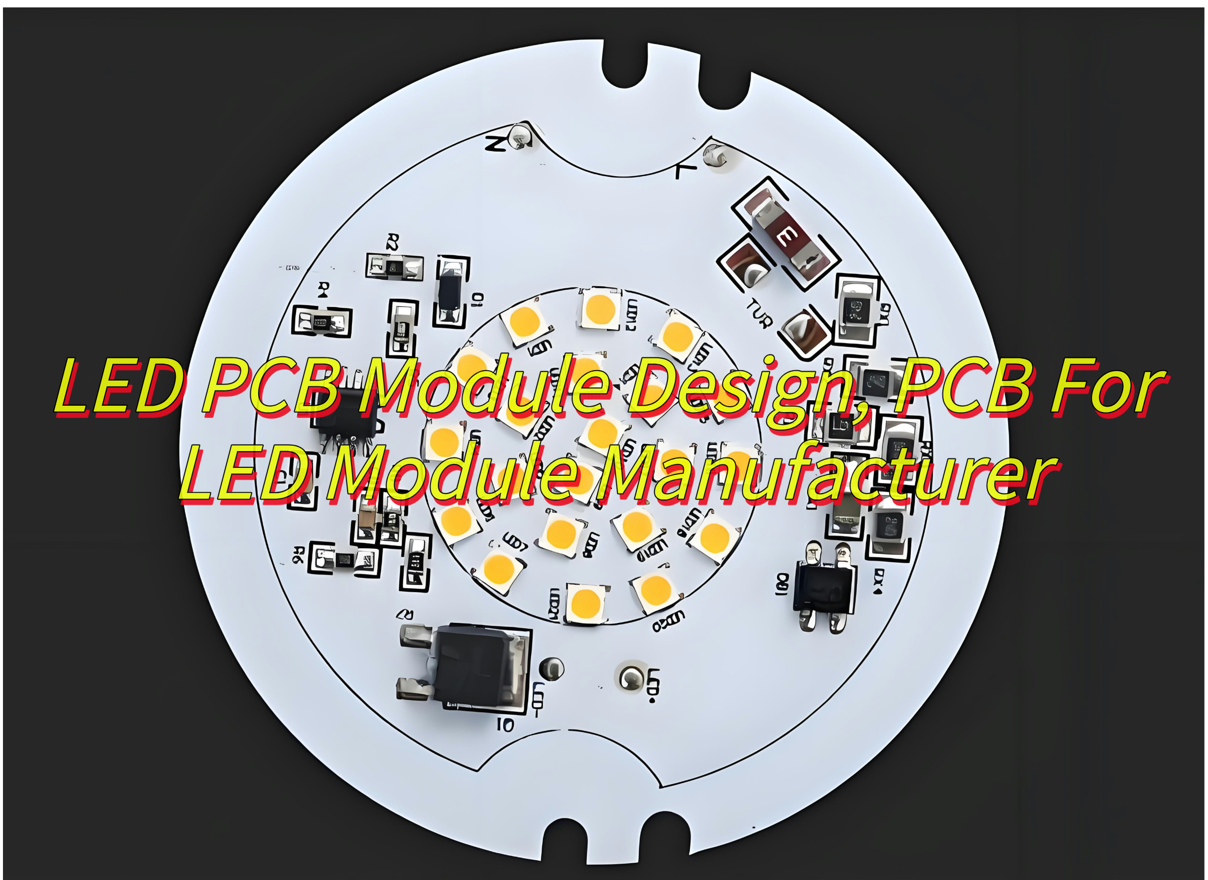
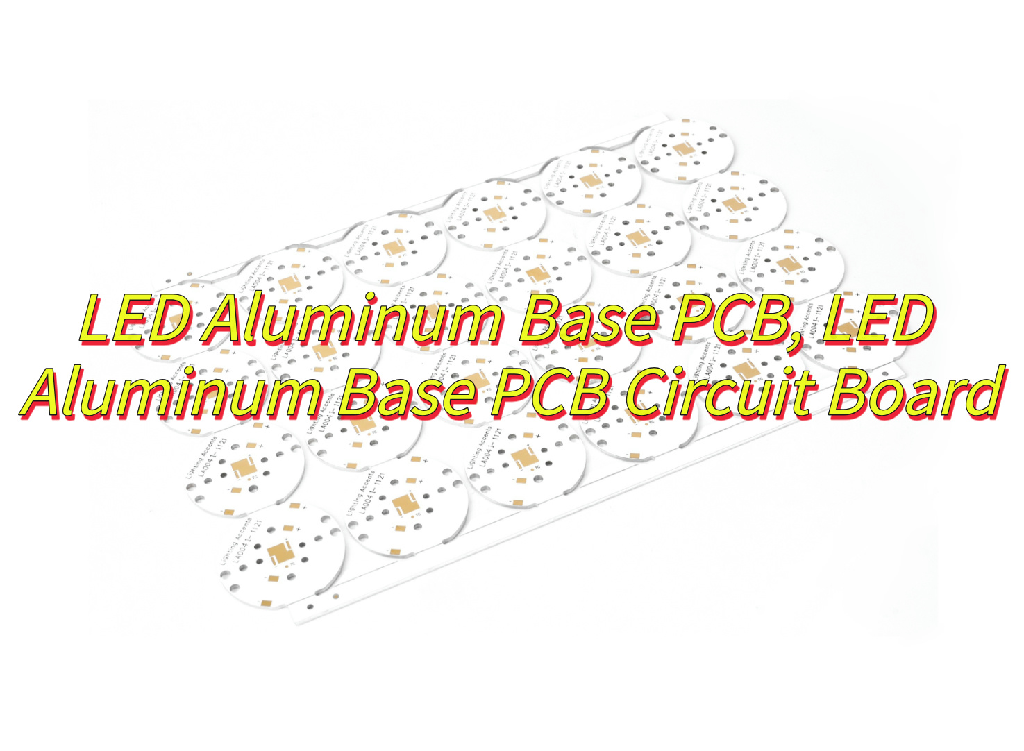
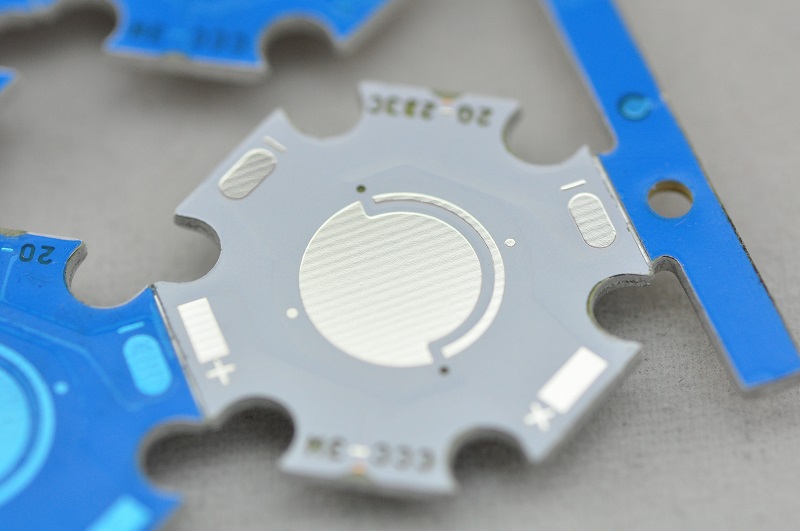
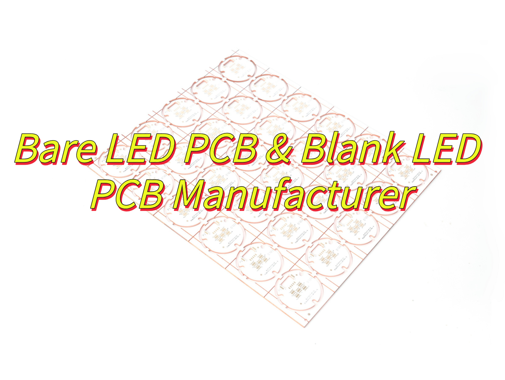
What Is A Bare LED PCB?
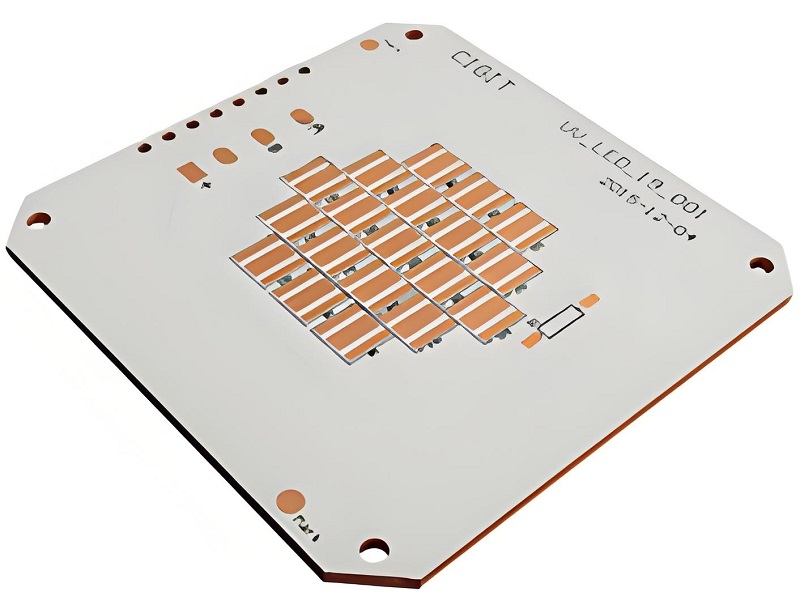
A bare LED PCB, also referred to as a blank LED PCB, is an unpopulated printed circuit board engineered exclusively for LED applications. It functions as the base platform for assembling LED components, providing structural integrity, electrical connectivity, and thermal dissipation. Typically manufactured from aluminum substrates (e.g., 6061-T6 alloy) or FR-4 laminates with enhanced thermal conductivity, this board type is designed to manage heat generated by high-power LEDs. It features pre-defined footprints for LED packages, solder pads for drivers, and thermal vias to optimize heat transfer. Unlike finished LED modules, it lacks mounted components, allowing flexibility in selecting resistors, capacitors, or optical coatings tailored to specific use cases. Common applications include lighting fixtures, automotive indicators, and display panels, where its durability and adaptability ensure reliable performance in environments requiring efficient heat management and electrical stability.
What Are Component of Bare LED PCB?
Components of a Bare LED PCB:
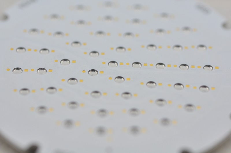
Substrate Material
- Typically aluminum (e.g., 6061-T6 alloy) or FR-4 laminate, chosen for thermal conductivity (1.0–2.5 W/m·K) and mechanical rigidity. Aluminum substrates excel in high-power LED applications due to their ability to dissipate heat efficiently.
Conductive Layer (Copper Traces)
- A thin copper foil layer (1–2 oz thickness) etched into circuits to route electrical signals. Trace widths and spacing are optimized to minimize voltage drop and resistive losses, especially in LED drivers.
Dielectric Insulation Layer
- A thermally conductive but electrically insulating layer (e.g., prepreg or ceramic-filled polymers) bonded between the substrate and copper traces. It prevents electrical shorts while transferring heat to the substrate.
Thermal Vias and Pads
- Plated holes or pads designed to enhance heat transfer from LED junctions to the substrate. Larger via diameters (≥0.5mm) and denser arrays improve thermal performance in high-wattage designs.
Solder Mask Coating
- A protective polymer layer (e.g., LPI or dry film) applied to prevent solder bridging and oxidation. It exposes only critical areas like component pads, ensuring precise assembly.
Surface Finish
- A metallic coating (e.g., HASL, ENIG, or Immersion Silver) to protect copper traces from corrosion and improve solderability. ENIG is preferred for LED PCBs due to its flatness and long-term reliability.
Mounting Holes and Fixtures
- Pre-drilled holes or slots for securing the PCB to heatsinks, enclosures, or optical lenses. Thread-forming screws or press-fit pins ensure mechanical stability in vibration-prone environments.
White Solder Mask (Optional)
- A light-reflective solder mask color to enhance luminous efficacy by redirecting stray light toward the LED emission surface, common in lighting applications.
Edge Connectors or Gold Fingers
- Plated edges for inter-PCB connectivity in modular designs (e.g., LED video walls), ensuring low-resistance signal transmission between adjacent modules.
Test Points and Fiducial Markers
- Exposed copper pads for in-circuit testing (ICT) and automated optical inspection (AOI). Fiducials aid precise component placement during SMT assembly.

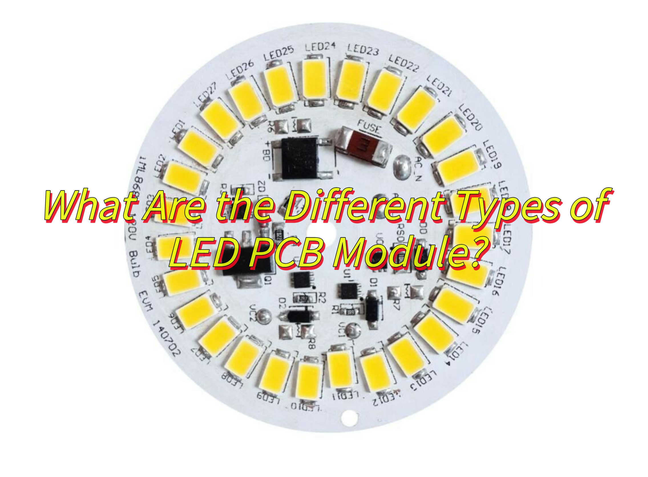
What Are Types of Blank LED PCB?
Types of blank LED PCBs categorized by layer count include:
Single-Layer Blank LED PCB
- Contains only one conductive copper layer on a single substrate side.
- Suitable for simple LED circuits with minimal component density.
- Cost-effective for basic lighting applications.
Double-Layer Blank LED PCB
- Features conductive layers on both top and bottom sides of the substrate, interconnected through vias.
- Provides higher routing flexibility than single-layer PCBs, supporting moderate-complexity LED designs.
- Commonly used in consumer electronics and automotive lighting.
Multilayer Blank LED PCB
- Comprises 4, 6, 8, or more layers, with alternating conductive and insulating layers bonded together.
- Utilizes blind vias, buried vias, or through-hole vias for interlayer connections.
- Ideal for high-density LED arrays, advanced thermal management, and high-frequency applications (e.g., industrial lighting, smart devices).
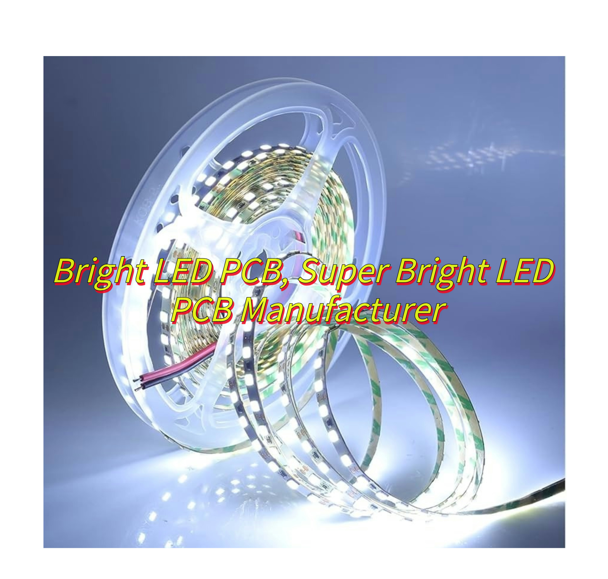
What Are Advantages of Bare LED PCB?
Advantages of Bare LED PCB:
Superior Thermal Management
- Metal-core substrates (e.g., aluminum) efficiently dissipate heat generated by high-power LEDs, reducing junction temperatures and extending lifespan. This prevents lumen depreciation and color shift in lighting applications.
Cost Efficiency at Scale
- Blank LED PCBs lower per-unit costs when ordered in bulk, making them ideal for mass-produced products like LED bulbs, strips, and signage. Standardized manufacturing processes minimize setup fees.
Design Flexibility
- Engineers can customize trace layouts, component placement, and thermal via patterns to optimize performance for specific use cases (e.g., high-voltage LED drivers or compact automotive modules).
Enhanced Durability
- Metal or ceramic substrates resist warping, vibration, and thermal cycling better than FR-4 boards, ensuring reliability in automotive headlights, industrial fixtures, and outdoor displays.
Improved Electrical Performance
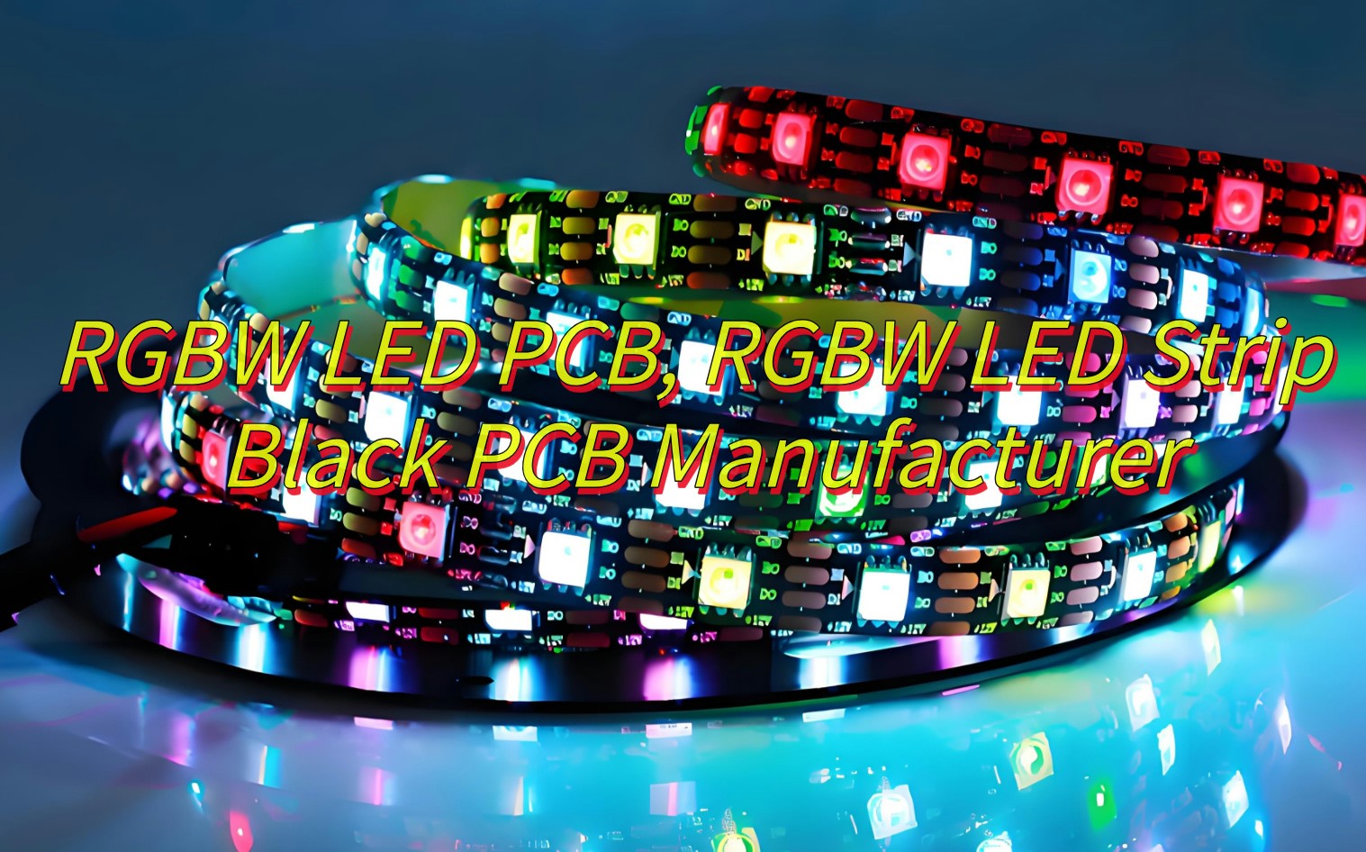
- Thick copper layers (2–3 oz) reduce resistive losses, while ground planes minimize electromagnetic interference (EMI). This is critical for RGBW LED controllers and smart lighting systems.
Environmental Resistance
- Many blank LED PCBs feature conformal coatings or immersion gold finishes to withstand moisture, dust, and chemicals, making them suitable for harsh environments like agricultural grow lights.
Compact Form Factors
- Multilayer designs enable high component density without sacrificing thermal performance, enabling slimmer LED fixtures for architectural lighting or wearable devices.
Faster Time-to-Market
- Standardized blank PCBs reduce prototyping lead times. Manufacturers often stock common sizes (e.g., 100x100mm), allowing rapid customization with minimal tooling adjustments.
Compliance with Safety Standards
- Blank LED PCBs are engineered to meet UL, IEC, or RoHS requirements, simplifying certification for lighting products sold in global markets.
Energy Efficiency
- By minimizing thermal losses and voltage drops, blank LED PCBs improve overall system efficiency, reducing energy consumption in commercial lighting installations.

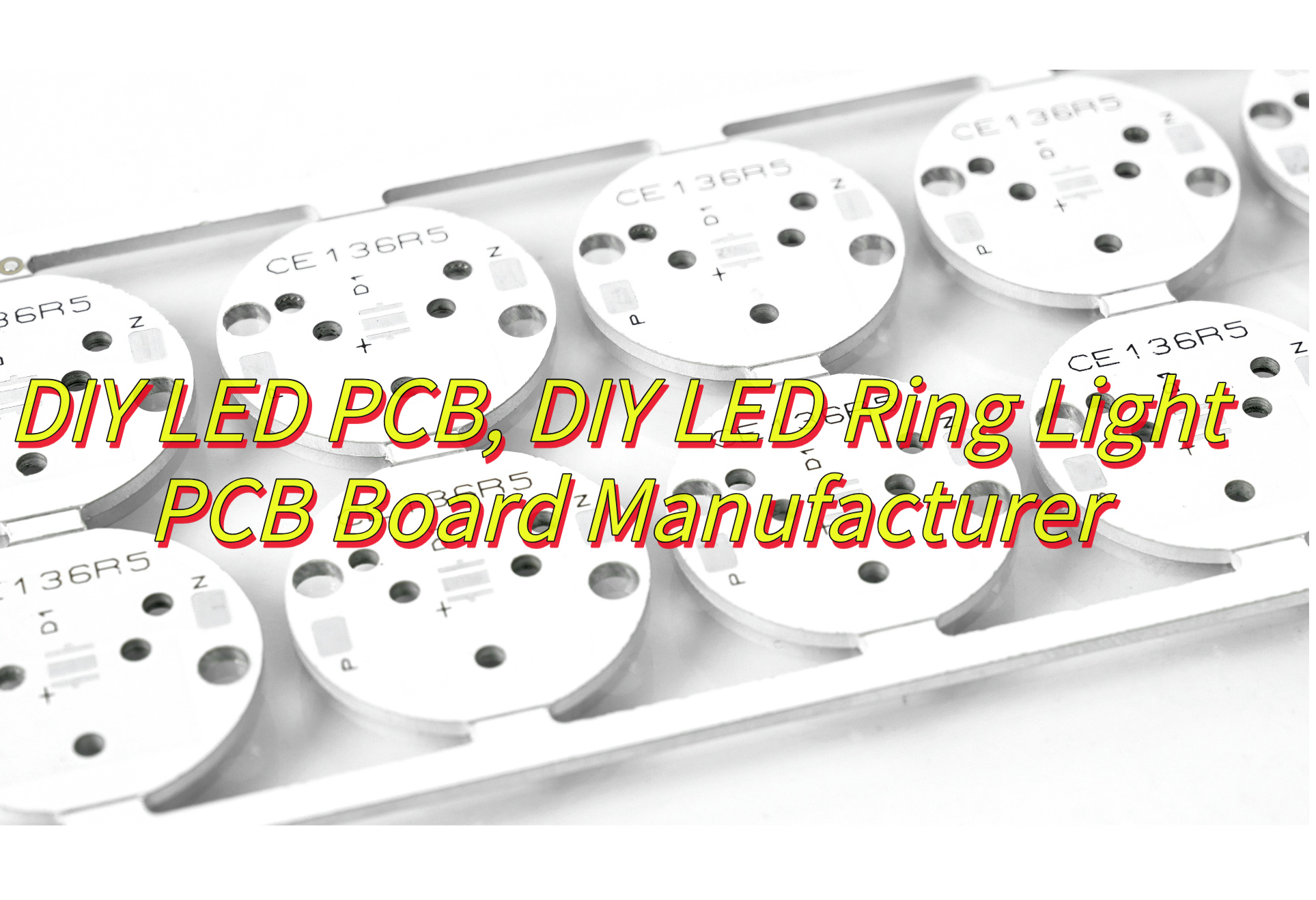
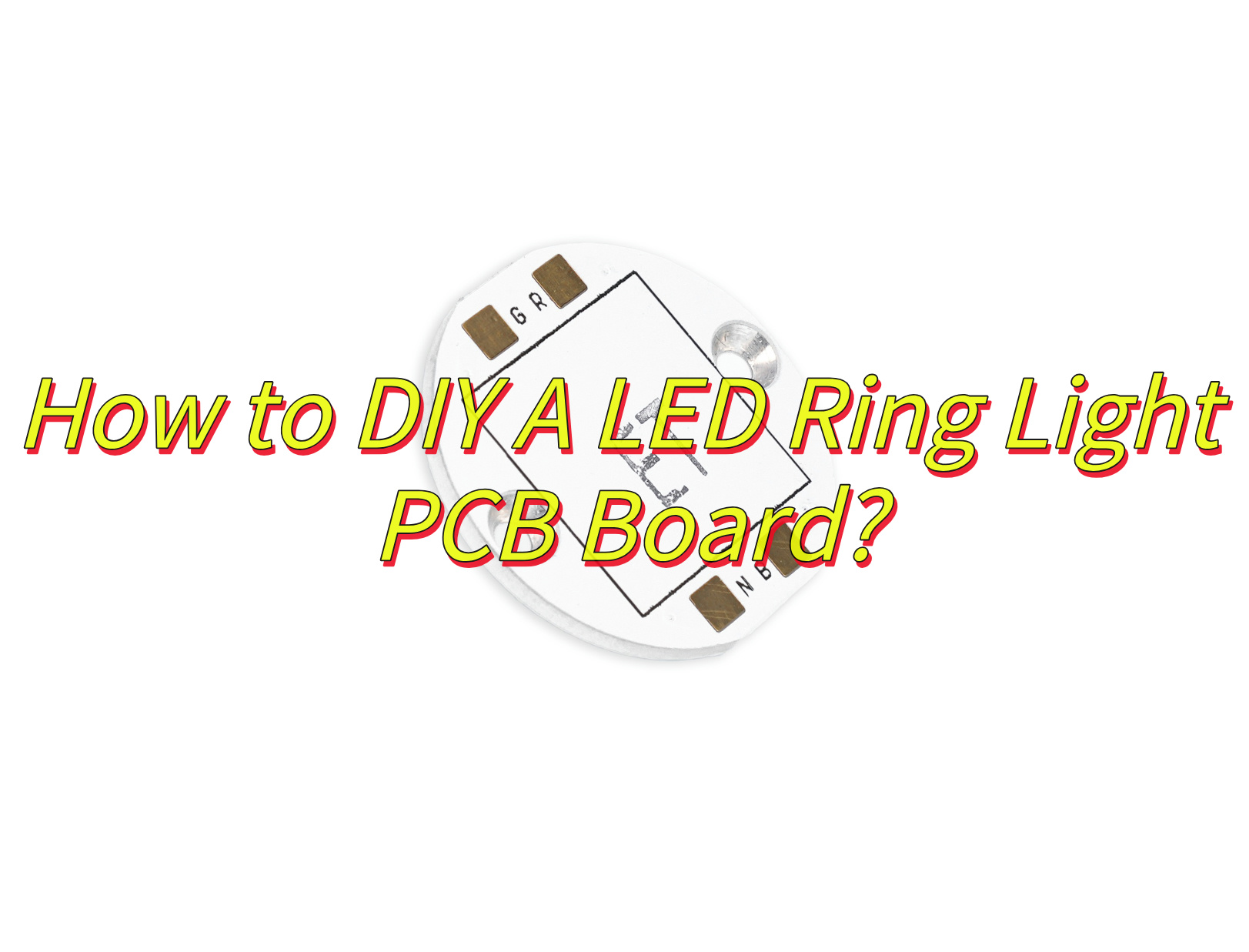
How to Make A Large 8×8 LED Matrix Bare PCB?
This is how to make a large 8×8 LED matrix bare PCB:
1. Design the PCB Layout
- Use EDA software (e.g., Altium, Eagle, or KiCad) to create a schematic and layout.
- Arrange 64 LED pads in an 8×8 grid with equal spacing (e.g., 5mm pitch for standard LEDs).
- Include row and column traces routed to edge connectors (e.g., 0.1″-pitch headers) for external control.
- Add thermal vias beneath LED pads to improve heat dissipation, especially for high-brightness LEDs.
2. Select Substrate Material
- Aluminum-Core PCB: Ideal for high-power matrices (e.g., 1W LEDs) due to its thermal conductivity (1.5–2.0 W/m·K).
- FR-4: Suitable for low-power indicators (e.g., 0.2W LEDs) where cost is prioritized.
- Ceramic (Alumina): Recommended for UV LEDs or harsh environments requiring chemical resistance.
3. Define Trace Widths and Spacing
- Calculate trace widths using a PCB calculator to handle current demands (e.g., 20-mil traces for 1A rows).
- Maintain ≥0.2mm spacing between traces to prevent short circuits during soldering.
4. Incorporate Mounting and Alignment Features
- Add fiducial markers (e.g., 1mm diameter copper pads) for precise SMT assembly.
- Include mounting holes (e.g., 3.2mm diameter) at corners for securing to heatsinks or enclosures.
5. Specify Surface Finish and Solder Mask
- ENIG (Electroless Nickel Immersion Gold): Ensures solderability and protects copper from oxidation.
- White Solder Mask: Enhances light reflectivity by 15–20% compared to traditional green masks.
6. Generate Manufacturing Files
- Export Gerber files (RS-274X format) for all layers: top copper, solder mask, silkscreen, and NC drill.
- Include a BOM (Bill of Materials) specifying LED footprint dimensions (e.g., 5050 SMD) and resistor values.
7. Collaborate with a PCB Manufacturer
- Choose a vendor with experience in LED matrix production and ISO 9001/UL certification.
- Request a DFM (Design for Manufacturability) review to identify potential issues (e.g., trace acid traps).
8. Quality Control Checks
- Electrical Testing: Verify continuity of rows/columns using flying probe or bed-of-nails fixtures.
- Thermal Imaging: Confirm uniform heat distribution across the matrix under full load.
- Visual Inspection: Check for solder mask defects, misaligned pads, or exposed copper.
9. Optional Enhancements
- Blackened Copper: Reduces light leakage between LEDs in display applications.
- Embedded Resistors: Integrate current-limiting resistors beneath LED pads to save space.
10. Packaging and Shipping
- Request vacuum-sealed packaging with desiccant to prevent moisture absorption during transit.
- Include a first-article sample for pre-production validation before bulk orders.
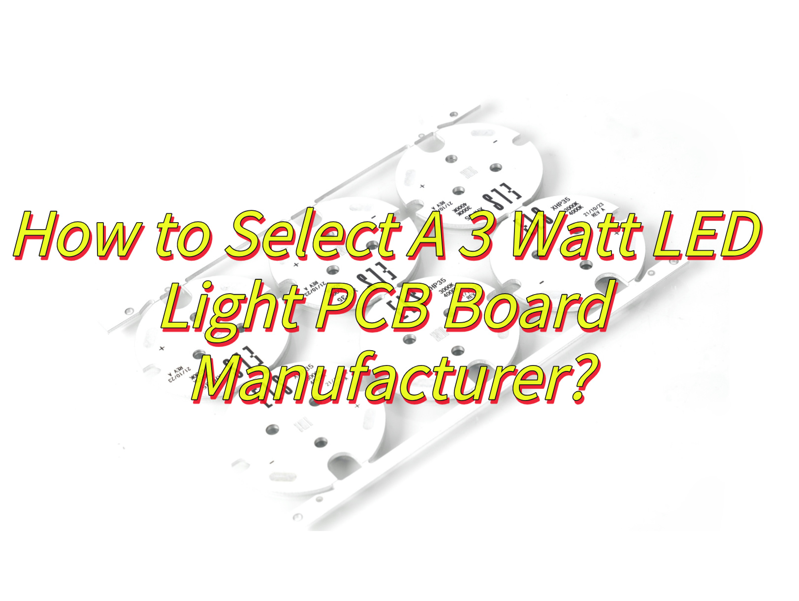
How to Evaluate A Reliable Bare LED PCB Manufacturer?
This is how to evaluate a reliable bare LED PCB manufacturer:
Verify Rapid Prototyping Capabilities
- 24-Hour Turnaround: Prioritize manufacturers offering 24-hour bare board fabrication for 1–6 layer PCBs, enabling fast design validation.
- 48-Hour Assembly: Look for suppliers capable of assembling prototypes within 48 hours, including SMT placement and through-hole components.
Assess Mass Production Lead Times
- Standard Delivery: Confirm 5–7 day lead times for standard orders (up to 16 layers) and 12–15 days for high-volume batches (10,000+ units).
- Expedited Options: Inquire about rush services (e.g., 3–5 day delivery for urgent orders) and associated surcharges.
Review Production Flexibility
- Layer Compatibility: Ensure the manufacturer supports 1–49 layer boards, including aluminum/MCPCB for thermal management.
- Material Options: Confirm availability of FR-4, Rogers, and ceramic substrates to match your application’s thermal/electrical needs.
Examine Quality Control for Speed
- Automated Testing: Require 100% electrical testing (ICT/flying probe), AOI, and X-ray inspection to catch defects without slowing production.
- Thermal Validation: Ensure thermal imaging is used to verify heat dissipation in high-power LED designs.
Check Design for Manufacturability (DFM) Support
- Engineering Review: A reliable manufacturer will analyze your Gerber files for trace widths, annular rings, and solder mask clearances to prevent delays.
- Impedance Control: For high-speed LED drivers, confirm they can meet tight impedance tolerances (e.g., 50Ω ±10%).
Evaluate Supply Chain Efficiency
- Component Sourcing: Inquire about in-house component procurement to avoid delays from third-party vendors.
- Inventory Management: Manufacturers with JIT (just-in-time) systems can reduce lead times by 20–30%.
Confirm Customization Speed
- Specialty Processes: Ensure they handle blind/buried vias, heavy copper (2–6 oz), and controlled impedance without extending lead times.
- Surface Finishes: Check availability of quick-turn ENIG, HASL, and OSP finishes to match your solderability requirements.
Analyze Pricing and Scalability
- Tiered Pricing: Compare quotes for prototypes (e.g., 50–200 per 10-piece batch) and bulk orders (e.g., 0.50–3.00 per unit at 10,000+).
- MOQ Flexibility: Look for suppliers accepting orders as low as 1 piece for prototyping and 50–100 pieces for production.
Audit Post-Sales Responsiveness
- 24/7 Support: Confirm availability of technical support for real-time troubleshooting during assembly.
- Warranty Terms: Ensure a minimum 1-year warranty covering delamination, solder joint failures, and material defects.
Leverage Customer Feedback
- Case Studies: Request examples of LED projects with similar complexity (e.g., 8×8 matrices, automotive headlights).
- References: Contact existing clients to validate on-time delivery rates (e.g., >95% for Tier 1 suppliers) and defect rates (<0.3%).

How Can Manufacturers Ensure Consistent Quality in Bare LED PCB Production?
Strict Material Qualification
- Certified Suppliers: Source substrates (e.g., aluminum, FR-4) from ISO-certified vendors with traceable lot numbers.
- Incoming Inspection: Test dielectric layers for thermal conductivity (≥1.5 W/m·K for metal-core boards) and copper foils for purity (99.9% minimum) using spectroscopy.
Design for Manufacturability (DFM) Reviews
- Automated Checks: Use software tools to validate trace widths, annular rings, and solder mask clearances against IPC standards.
- Thermal Simulation: Model heat dissipation using software like ANSYS Icepak to optimize via placement and substrate thickness.
Process Control and Automation
- Laminate Pressing: Maintain ±2°C temperature control during layer bonding to prevent delamination.
- Etching Precision: Use laser-direct imaging (LDI) for sub-50μm trace resolution, reducing undercutting risks.
- Drilling Accuracy: Employ CNC machines with ±25μm positional tolerance for via drilling.
Multi-Stage Inspection Protocols
- Automated Optical Inspection (AOI): Detect solder mask defects, missing pads, or copper shorts at 100% speed.
- X-ray Inspection: Verify via fills and inner-layer alignment for multilayer boards.
- Thermal Imaging: Identify hotspots under full load to validate thermal design.
Electrical Performance Testing
- Flying Probe Testing: Measure continuity and isolation resistance (≥100MΩ) for all nets.
- Impedance Control: Use TDR (Time-Domain Reflectometry) to validate ±10% tolerance for high-speed signals.
Environmental and Stress Testing
- Thermal Cycling: Subject boards to -40°C to +125°C cycles (500–1,000 iterations) to simulate long-term reliability.
- Humidity Resistance: Test at 85°C/85% RH for 168 hours to assess solder mask and laminate integrity.
Employee Training and Certification
- IPC-A-600 Certification: Ensure inspectors are trained to identify micro-cracks, voids, and other latent defects.
- Cross-Training: Rotate staff across processes (e.g., etching, plating) to maintain skill versatility.
Statistical Process Control (SPC)
- Real-Time Monitoring: Track parameters like etch time, plating thickness, and oven temperatures using IoT sensors.
- Control Charts: Flag out-of-spec variations (e.g., copper thickness >10% of target) for immediate corrective action.
Supplier Quality Management
- Scorecard System: Rate component vendors on delivery performance, defect rates, and compliance with RoHS/REACH.
- Joint Development: Collaborate with material suppliers to customize substrates for high-power LED applications.
Continuous Improvement Loop
- Failure Analysis: Use SEM (Scanning Electron Microscopy) to root-cause defects (e.g., copper voiding, solder mask peeling).
- PDCA Cycle: Implement Plan-Do-Check-Act methodologies to refine processes based on defect data.
What Factors Affect the Price of LED Bulb Blank PCB?
Factors Affecting the Price of LED Bulb Blank PCB
Substrate Material Cost
- Base Material: Aluminum-core PCBs (for thermal management) cost 20–30% more than FR-4 boards but offer superior heat dissipation.
- Copper Thickness: Thicker copper layers (2–3 oz vs. 1 oz) increase material costs by 15–20% but reduce resistive losses.
- Surface Finish: ENIG (Electroless Nickel Immersion Gold) adds 10–15% to costs compared to HASL (Hot Air Solder Leveling) due to gold plating.
PCB Size and Layer Count
- Board Dimensions: Larger PCBs (e.g., 100x100mm vs. 50x50mm) waste more substrate material, raising costs by 5–10% per panel.
- Layer Complexity: 4-layer boards cost 30–50% more than 2-layer designs due to additional lamination and drilling steps.
Manufacturing Volume
- Economies of Scale: Bulk orders (10,000+ units) reduce per-unit costs by 40–60% compared to prototypes (1–10 units).
- Setup Fees: Small batches incur higher tooling charges (e.g., 50–200 for stencils and fixtures).
Design Complexity
- Trace Density: Finer traces (<75μm) require laser-direct imaging (LDI), increasing costs by 10–15%.
- Via Types: Blind/buried vias add 20–30% to pricing due to multi-stage lamination and drilling.
Thermal Management Requirements
- Thermal Vias: Dense via arrays (e.g., 50+ vias per LED) add 5–8% to costs but improve heat dissipation.
- Heatsink Integration: PCBs with embedded copper heatsinks cost 25–40% more than standard designs.
Certifications and Compliance
- Safety Standards: UL 8750 or IEC 62776 certification adds 200–500 to testing fees per batch.
- RoHS Compliance: Lead-free solder and halogen-free laminates increase material costs by 8–12%.
Supply Chain Fluctuations
- Copper Prices: A 10% rise in global copper prices can increase PCB costs by 3–5%.
- Logistics: Air freight for rush orders adds 50–100% to shipping costs versus sea freight.
Quality Control Measures
- Testing: 100% electrical testing (flying probe) adds 0.10–0.30 per board, while X-ray inspection adds 0.20–0.50.
- Defect Warranties: Manufacturers offering 1-year replacement guarantees factor in 2–3% buffer for potential reworks.
Geographic Location
- Labor Costs: PCBs manufactured in China/Southeast Asia cost 30–50% less than in Europe/North America due to lower wages.
- Tariffs: Imports to regions like the EU or US incur 2–7% duties, impacting final pricing.
Lead Time Urgency
- Expedited Production: Rush orders (24–48 hours) incur 20–40% surcharges due to prioritized machine time and labor overtime.
By optimizing these factors (e.g., standardizing designs, selecting cost-effective materials, and consolidating orders), manufacturers can balance performance and affordability for LED bulb applications.