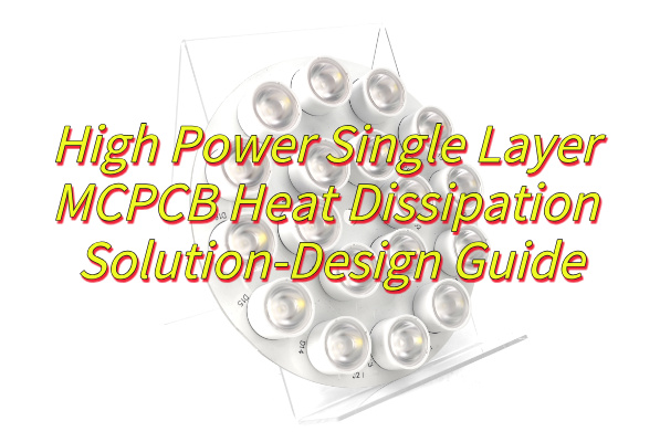
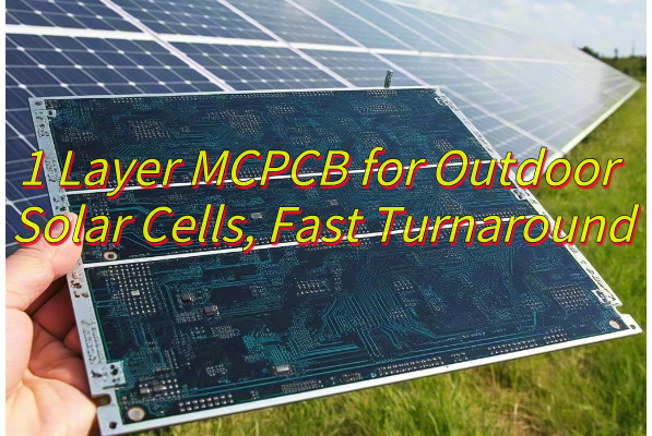
Why choose 1 Layer MCPCB for outdoor solar cells? This guide explores its structure, thermal advantages, and reliability enhancements for harsh environments.
Solar Energy Innovators: Are you struggling with:
- Heat-induced efficiency loss in outdoor solar arrays?
- Slow prototyping delaying your time-to-market?
- Environmental degradation shortening product lifespan?
EBest Circuit (Best Technology) Can Provide You:
- 24H rapid prototyping – accelerate R&D cycles
- Ultra-optimized thermal paths – 40% better heat dissipation vs standard boards
- Aerospace-grade durability – IP68 aluminum substrate withstands UV/moisture/salt spray
Request your free thermal simulation report today: sales@bestpcbs.com.
What Is A 1 Layer MCPCB?
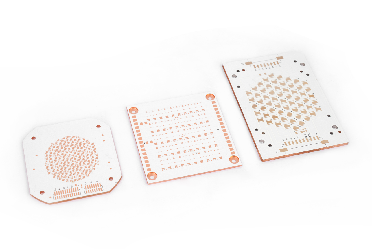
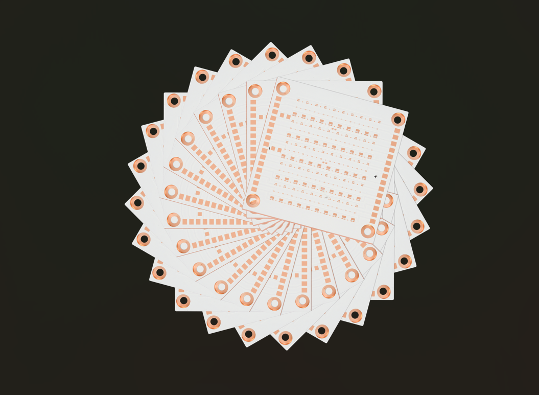
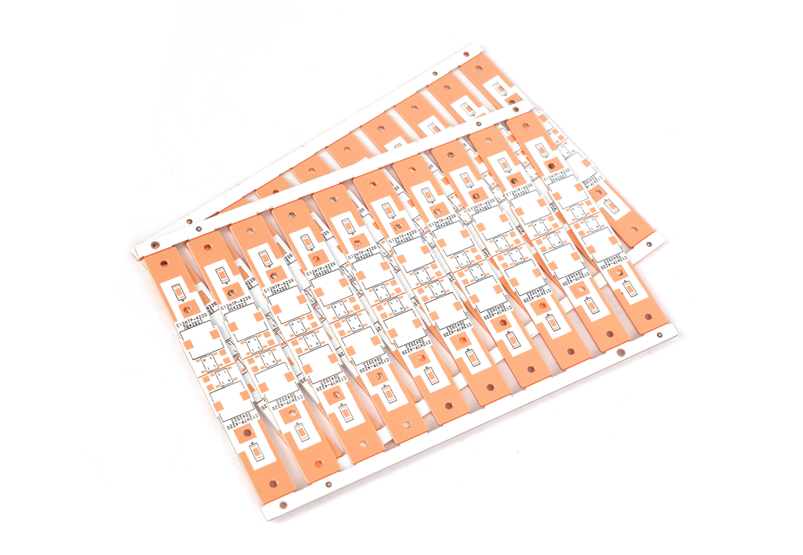
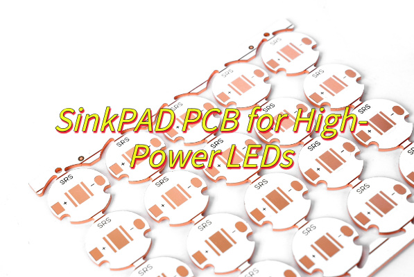
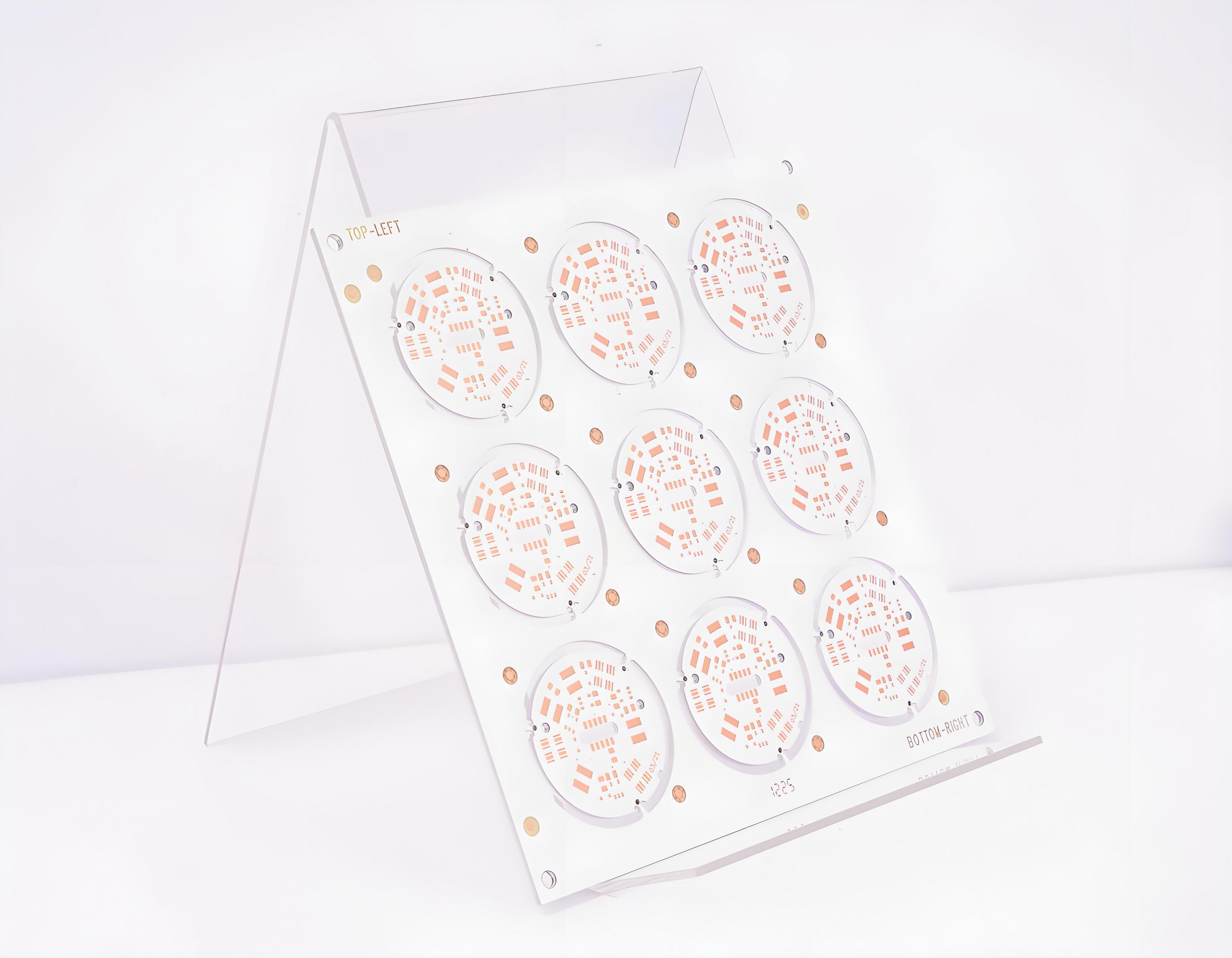
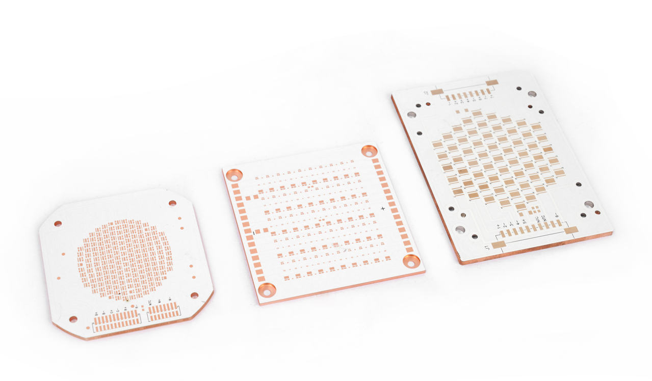
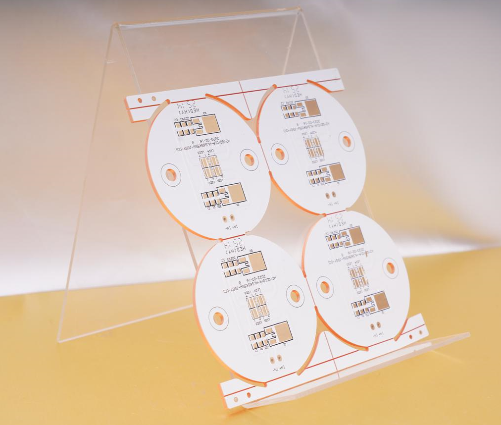
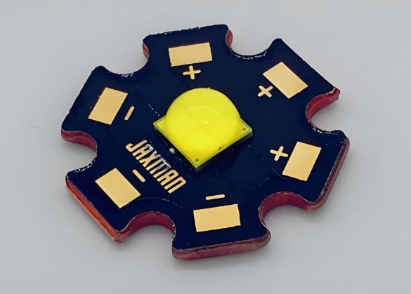
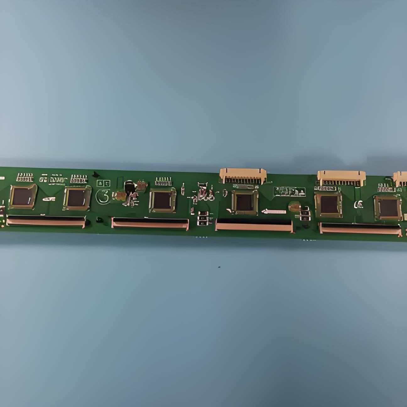
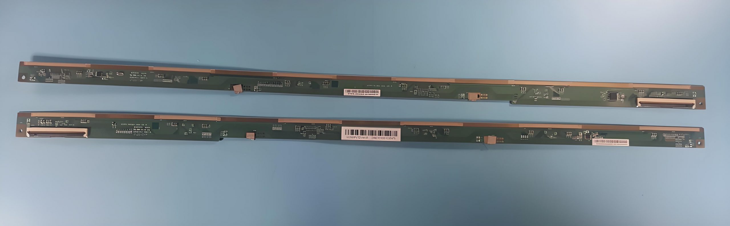
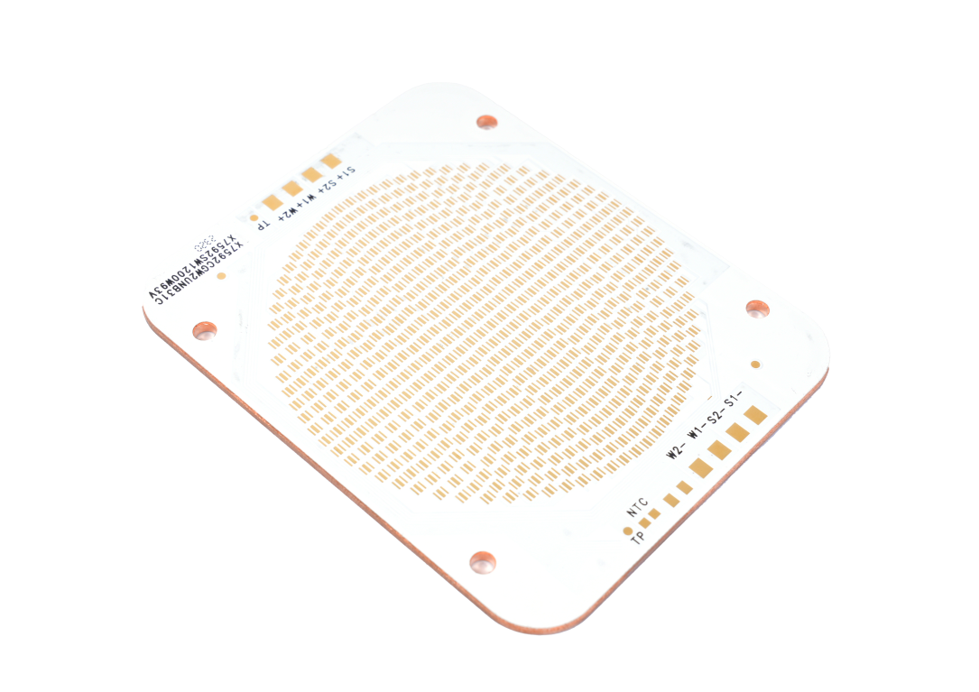
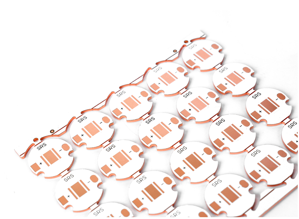
A 1 Layer MCPCB (Metal Core Printed Circuit Board) is a specialized circuit board featuring a single conductive copper layer bonded to a metal substrate, usually aluminum. The metal core efficiently transfers heat away from components, making it ideal for high-power applications where thermal management is essential.
The structure consists of three main parts: a metal base for heat dissipation, a dielectric layer for electrical insulation, and a single copper layer for circuitry. This design ensures effective cooling while maintaining electrical isolation. Though simpler than multi-layer boards, it offers excellent thermal performance for LED lighting, power electronics, and automotive systems.
With its straightforward layout, a 1 Layer MCPCB balances cost-effectiveness and reliability, making it a preferred choice for heat-sensitive electronics requiring durability and efficient thermal regulation.
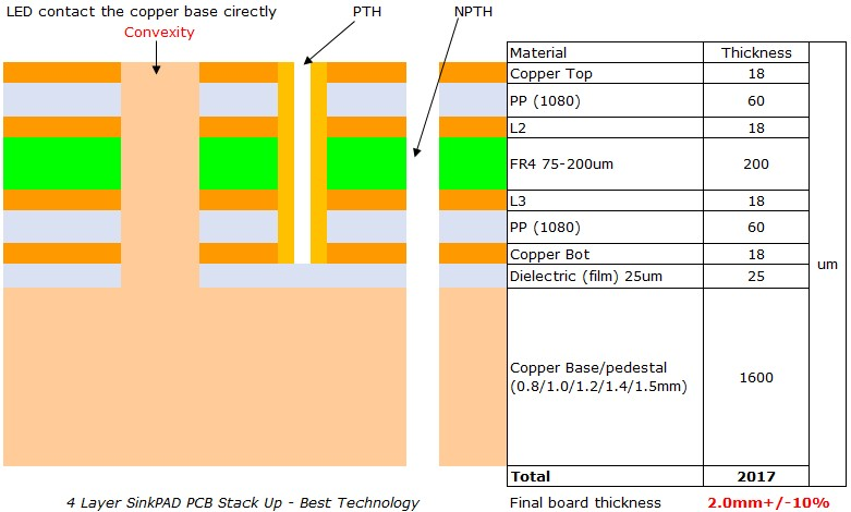
How thick Is a 1 layer MCPCB?
Here’s a structured breakdown of typical thickness specifications for a 1 Layer MCPCB:
Metal Core Thickness
- The base metal layer (usually aluminum) typically ranges from 1.0mm to 3.0mm, with 1.5mm and 2.0mm being most common for standard applications.
- Thicker cores (e.g., 3.0mm+) may be used for extreme heat dissipation needs.
Dielectric Layer Thickness
- The insulating layer between the metal core and copper ranges from 50µm to 150µm (0.05mm to 0.15mm).
- Thinner dielectrics improve heat transfer but require precise manufacturing.
Copper Layer Thickness
- The single conductive copper layer is commonly 1oz (35µm) or 2oz (70µm) but can go up to 3oz+ for high-current designs.
Overall Board Thickness
- Total thickness typically falls between 1.2mm to 3.2mm, depending on the combined layers.
- Example: A standard 1.5mm aluminum core + 100µm dielectric + 1oz copper ≈ 1.6mm total.
Customization Factors
- Thickness can be adjusted based on thermal, mechanical, or electrical requirements.
- Thinner boards suit compact designs, while thicker variants enhance rigidity and heat spreading.
What Is the Dielectric Layer of the 1 Layer MCPCB?
The dielectric layer in a 1 Layer MCPCB serves as the electrically insulating yet thermally conductive interface between the metal core and copper circuit layer. Here’s a structured breakdown of its characteristics:
- Primary Function: Electrically isolates the copper circuitry from the metal base (typically aluminum) while efficiently transferring heat from components to the metal core.
- Material Composition: Often consists of polymer-based composites (e.g., epoxy resins) filled with thermally conductive ceramics (alumina, boron nitride) to enhance heat dissipation.
- Thermal Performance: Anisotropic microstructures in advanced dielectric layers can improve thermal diffusivity by optimizing filler connectivity, reducing thermal resistance in high-power applications.
- Thickness Range: Typically measures 50–150µm (0.05–0.15mm), balancing electrical insulation and thermal transfer efficiency.
- Impact on LED Performance: Inefficient dielectric layers may lead to higher junction temperatures in LEDs, reducing luminous output and efficiency.
What Is the Use of 1 Layer MCPCB?
Uses of 1 Layer MCPCB:
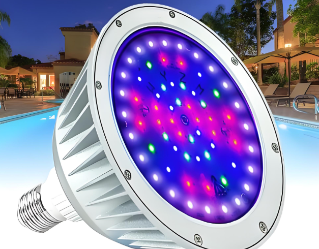
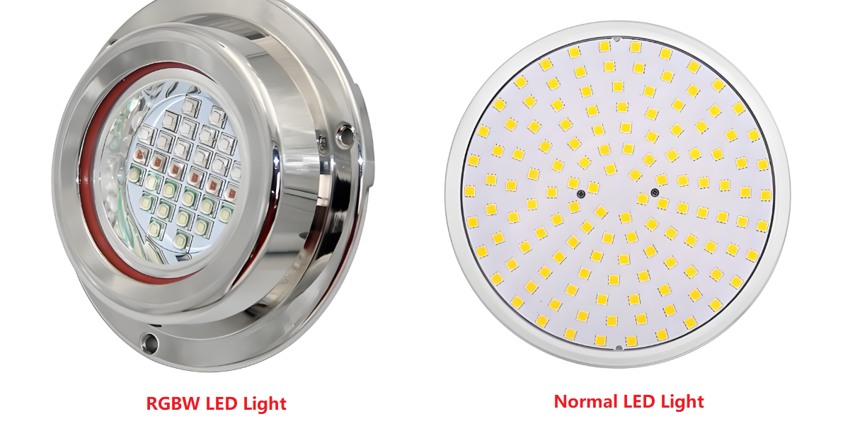
- High-Power LEDs – Directs heat away from LEDs, keeping them cool for brighter, longer-lasting light.
- Power Electronics – Manages heat in devices like inverters or motor drivers, ensuring stable performance under heavy loads.
- Automotive Systems – Withstands heat and vibrations in car lights or control units, even in tough conditions.
- RF/Microwave Devices – Reduces overheating in radios or antennas, maintaining clear signal strength.
- Solar Equipment – Keeps solar charge controllers or inverters efficient by handling sunlight-generated heat.
- Industrial Sensors – Durable design for factory sensors exposed to heat, dust, or movement.
- Compact Gadgets – Slim, heat-friendly boards for laptops or gaming devices with powerful chips.

Why Choose 1 Layer MCPCB for Outdoor Solar Cells?
- Heat Dissipation: Metal core efficiently conducts heat away from solar cells, preventing overheating and maintaining optimal conversion efficiency even under direct sunlight.
- Temperature Stability: Withstands outdoor temperature fluctuations, reducing thermal stress on components and ensuring consistent performance during day-night cycles.
- Durability in Harsh Conditions: Resists moisture, dust, and UV exposure, making it suitable for long-term outdoor use without degradation.
- Cost-Effective Design: Simpler structure lowers production costs while still delivering reliable thermal management for solar applications.
- Enhanced Lifespan: By keeping components cooler, it reduces wear and tear, extending the operational life of solar charging systems or inverters.
How to Enhance 1 Layer MCPCB Heat Dissipation to Extend Outdoor Solar Cells Lifespan?
- Choose High-Conductivity Substrates: Use copper (385 W/m·K) for the metal core if weight allows. For lighter builds, select 1.5mm+ thick aluminum (237 W/m·K) with a matte finish to boost radiative cooling under sunlight.
- Use Advanced Dielectric Materials: Replace standard epoxy with ceramic-filled polyimide (1.5–3 W/m·K) in the insulating layer. This cuts thermal resistance by 40–60%, accelerating heat transfer to the substrate.
- Maximize Thermal Via Efficiency: Drill 0.3mm copper-plated vias beneath heat-generating components (e.g., diodes, MPPT chips) at 1mm spacing. Arrange vias in a grid pattern to create vertical heat pathways.
- Integrate Passive Cooling Elements: Attach finned aluminum heat sinks (10–20mm tall) to the MCPCB’s backside. In compact spaces, use graphite sheets (1,500 W/m·K) or vapor chambers to spread heat evenly across the substrate.
- Apply Emissivity-Enhancing Coatings: Coat the metal core’s exterior with black ceramic paint (emissivity >0.85). This increases infrared radiation, helping the board shed heat faster under direct solar exposure.
- Optimize Component Layout: Place high-power components (e.g., transistors) away from solar cell active zones. Use thermal gap pads (2–4W/m·K) to ensure direct contact between parts and the MCPCB surface.
- Validate with Thermal Modeling: Use ANSYS Icepak or similar tools to simulate heat flow. Adjust via patterns, material thickness, or component positions based on hotspot analysis (e.g., reduce via spacing in 50°C+ zones).
How to Improve 1-Layer MCPCB Reliability for Outdoor Solar Cells?
Select Durable Materials
- Use aluminum (lightweight, corrosion-resistant) or copper (high conductivity) for the metal core. Pair with polyimide or modified epoxy dielectric layers to resist moisture and delamination while ensuring efficient heat transfer.
Boost Thermal Performance
- Increase thermal via density under high-heat components (e.g., solar charge controllers) to direct heat to the metal base. Thicken the substrate (e.g., 2mm aluminum) or add external heat sinks for passive cooling, reducing active system reliance.
Apply Protective Coatings
- Coat circuits with UV-resistant, waterproof conformal coatings (e.g., silicone for coastal areas) to shield solder joints and traces from humidity, dust, and salt spray.
Use Robust Components
- Choose outdoor-rated parts (e.g., capacitors rated for -40°C to 125°C) and high-reliability solder (e.g., SAC305).
Strengthen Design and Test
- Match dielectric layer CTE to metal and copper traces to prevent cracking. Secure edges with epoxy or fasteners for vibration resistance. Validate with 1,000+ hours of 85°C/85%RH damp heat, thermal shock (-40°C to 125°C), and salt-spray tests.
How to Enhance 1-layer MCPCB Durability for Harsh Outdoor Conditions?
Use Corrosion-Resistant Substrates
- Select anodized aluminum (5052 alloy) for coastal or industrial areas. Anodizing creates a 5–25µm oxide layer that resists salt and moisture. In extreme corrosion environments, choose 316 stainless steel despite its higher weight.
Apply Multi-Layer Protective Coatings
- Coat circuits with a 50–100µm silicone-based layer (e.g., Dow Corning 1-2577) to block moisture and dust. Add a 20–30µm acrylic topcoat for scratch resistance, focusing on solder joints and exposed traces.
Reinforce Mechanical Stability
- Thicken the dielectric layer to 100µm polyimide to reduce flexing under thermal stress. Secure board edges with epoxy adhesive or aluminum brackets to prevent warping from temperature swings (-40°C to 125°C) or vibration.
Choose Outdoor-Rated Components
- Use IP67-rated capacitors, resistors, and connectors with a -40°C to 125°C operating range. Select gold-plated contacts for connectors to resist tarnishing in humid environments.
Match Thermal Expansion Properties
- Select dielectric layers with a coefficient of thermal expansion (CTE) close to aluminum (23–24 ppm/°C). Ceramic-filled polyimide (CTE 12–18 ppm/°C) reduces stress on copper traces during temperature fluctuations.
Validate with Accelerated Aging
- Perform 2,000-hour thermal cycling (-40°C to 125°C, 1-hour dwells) and 96-hour salt-spray tests (ASTM B117). Include UV exposure (ISO 4892-3) to confirm coating integrity under prolonged sunlight.
Conclusion
In summary, 1 layer MCPCBs provide an efficient thermal management solution for outdoor solar cells with their optimized metal core structure, dielectric layer design, and enhanced durability features. By improving heat dissipation through material selection and layout optimization, these boards significantly extend solar cell lifespan while withstanding harsh environmental conditions. For projects requiring fast turnaround and reliable performance, our customized 1-layer MCPCB solutions offer the perfect balance of cost-effectiveness and thermal efficiency. Contact us today for a competitive quote: sales@bestpcbs.com.