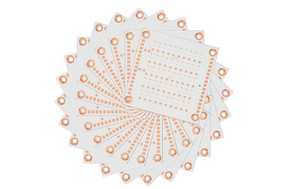
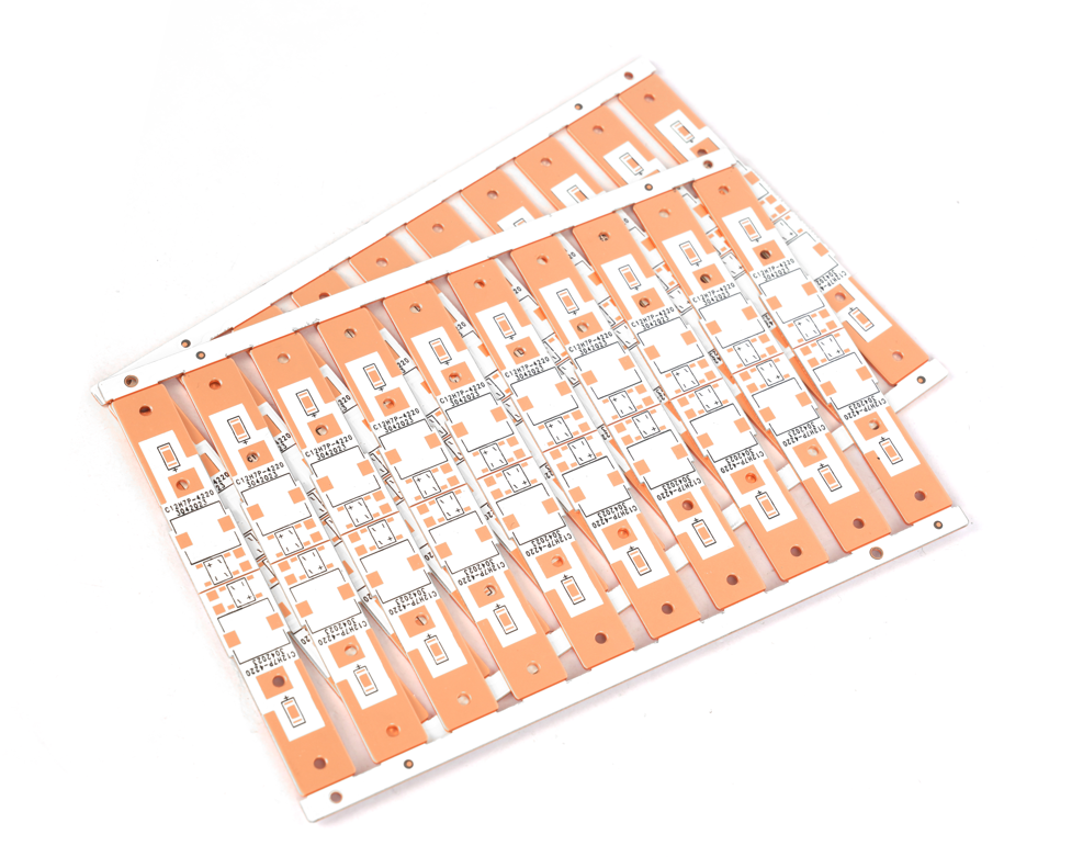
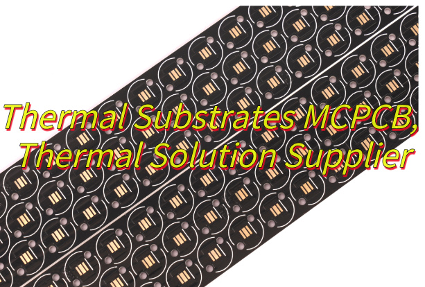
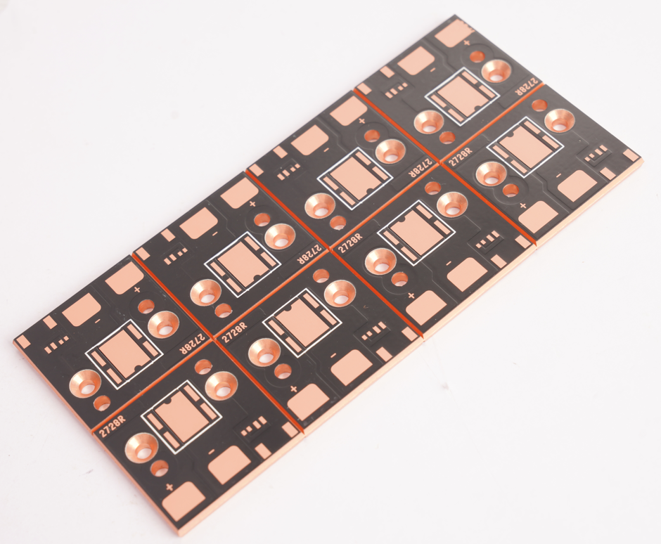
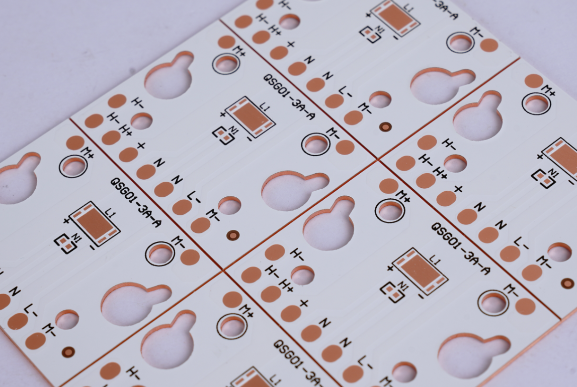
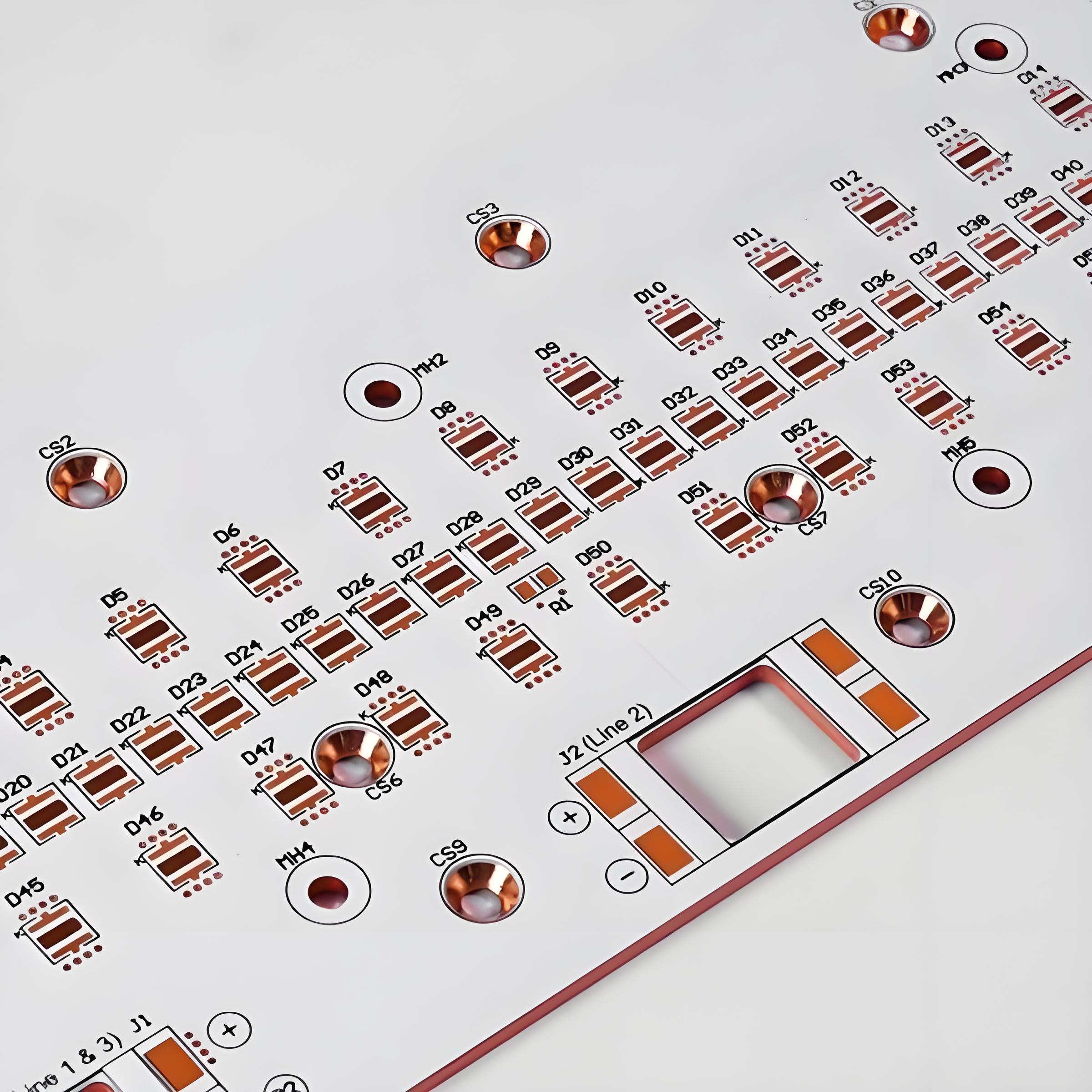
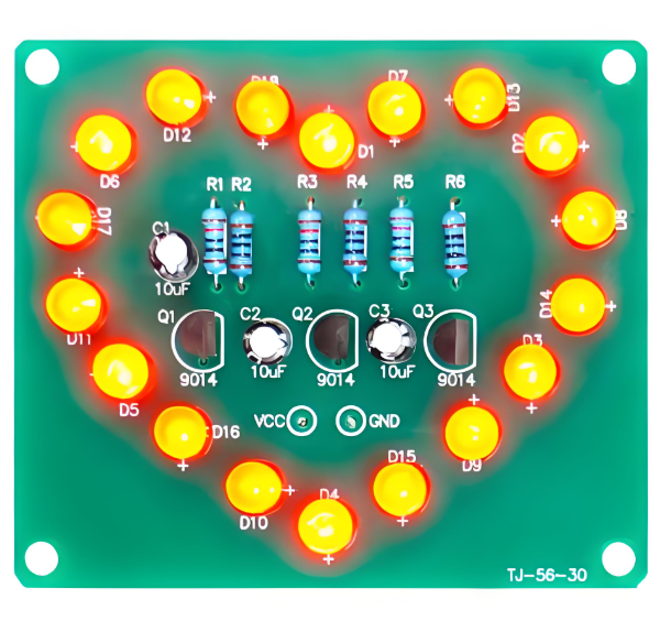
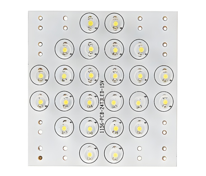
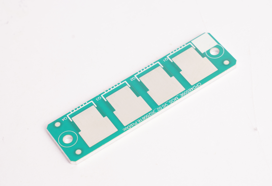
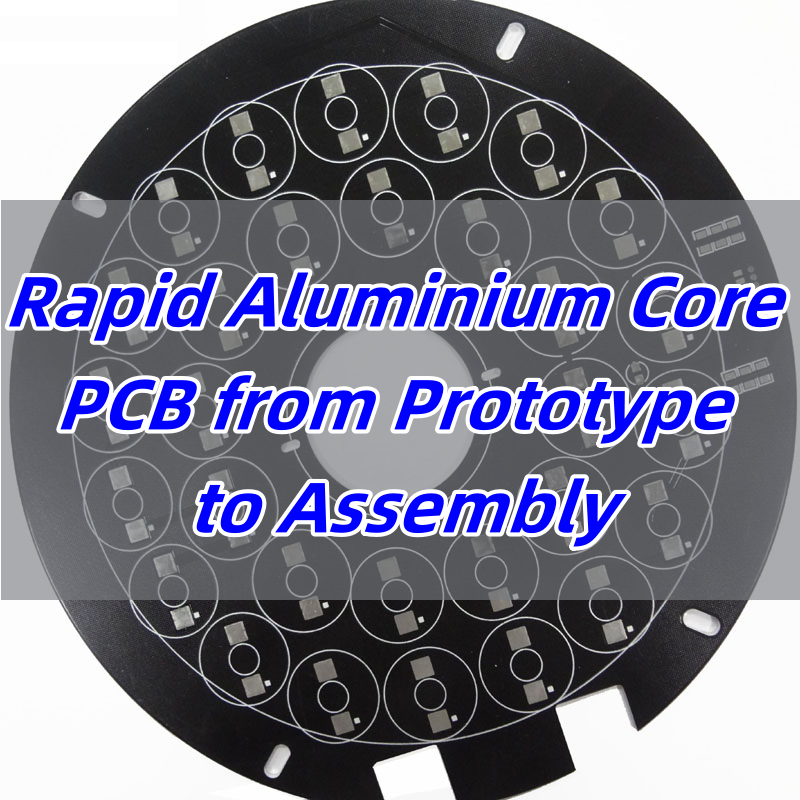
Aluminium core PCB is a popular choice for engineers who need fast heat dissipation, stable performance, and quick turnaround from prototype to full assembly. These boards simplify thermal management, especially in LED and power applications.
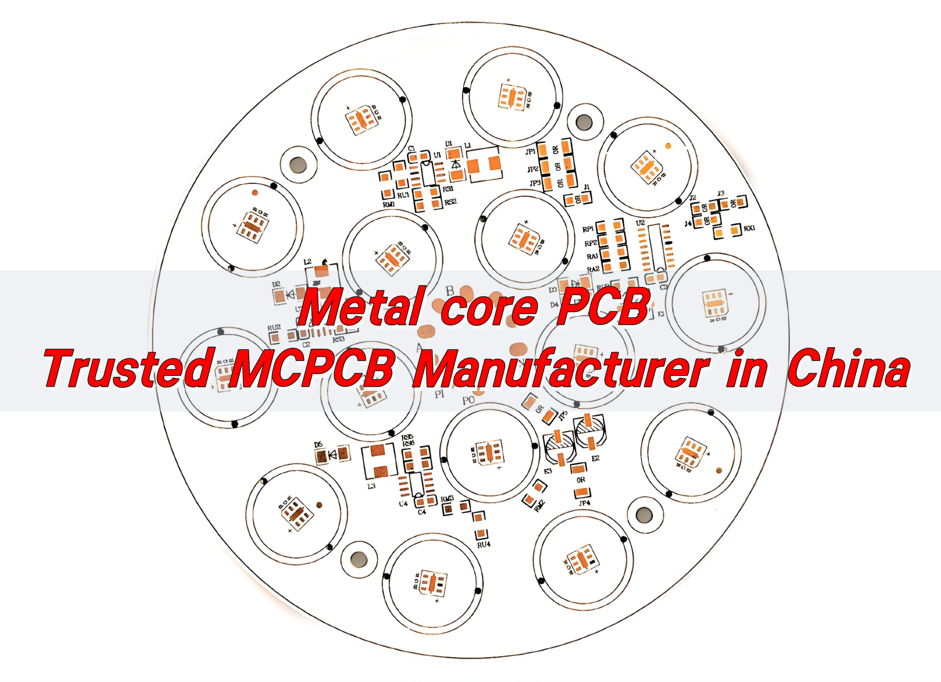
EBest Circuit (Best Technology) is a metal core PCB manufacturer in China, offering DFM analysis, 24-hour prototyping, high-quality aluminum core PCBs fabrication, and SMT service to the extremely competitive market since 2006. Our engineers have the hands-on experience to solve challenges like drilling precision, soldering failures, grounding instability, thermal expansion mismatch, lead time pressures, and quality control and defect management. If you require rapid aluminium core PCB from prototype to assembly, please contact us via email sales@bestpcbs.com.
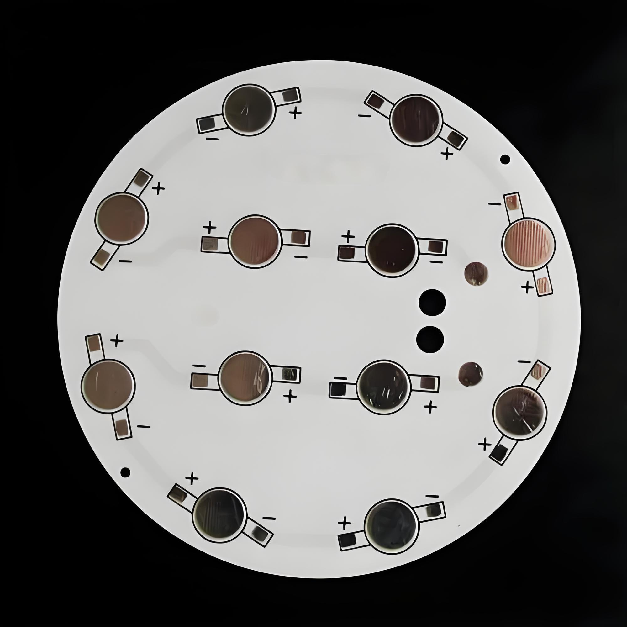
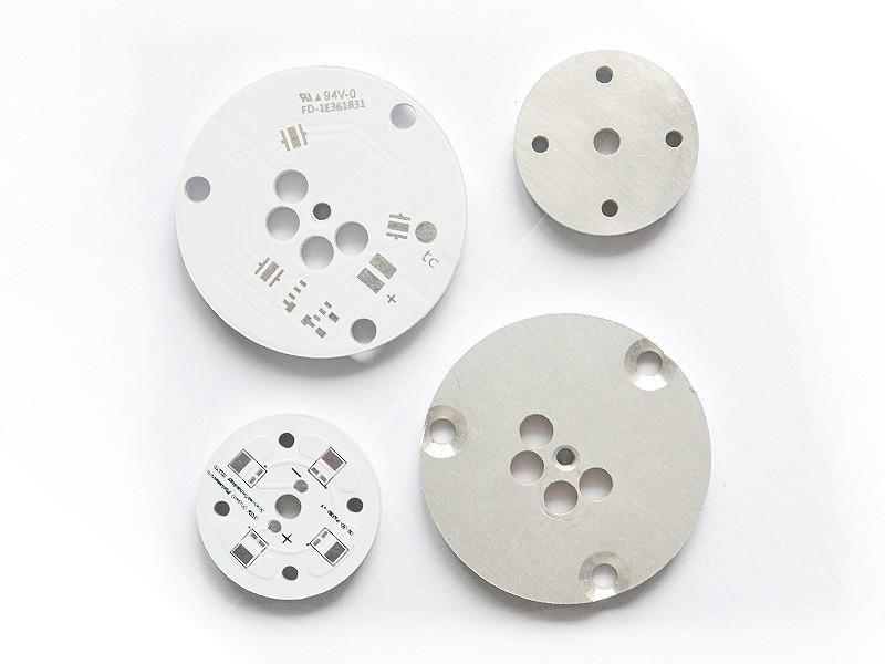
What is Aluminium Core PCB?
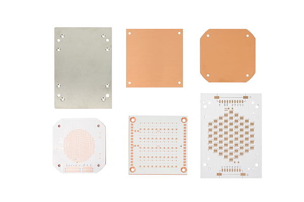
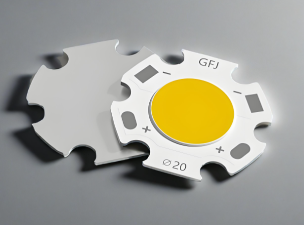
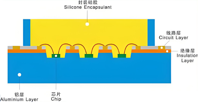
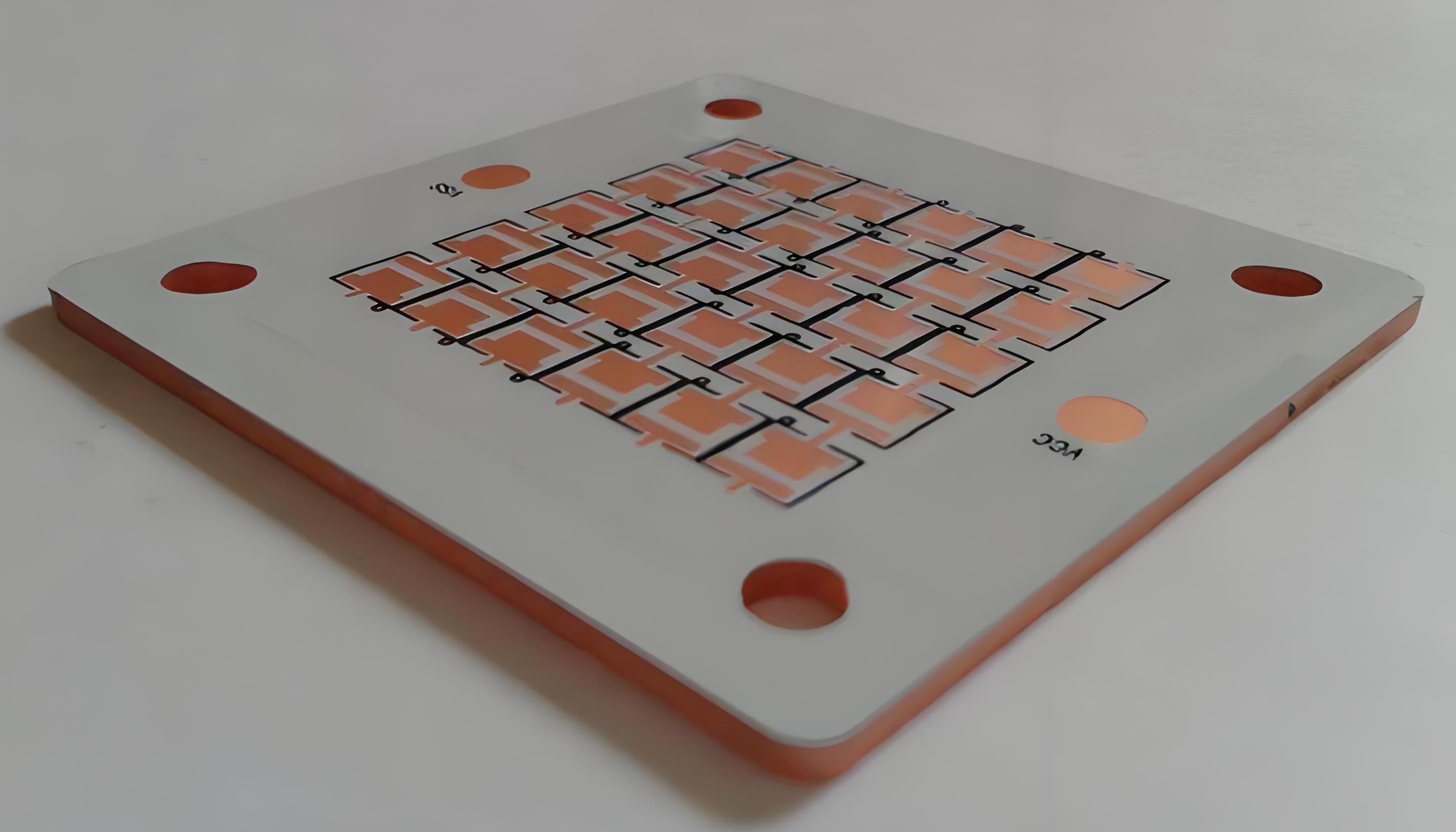
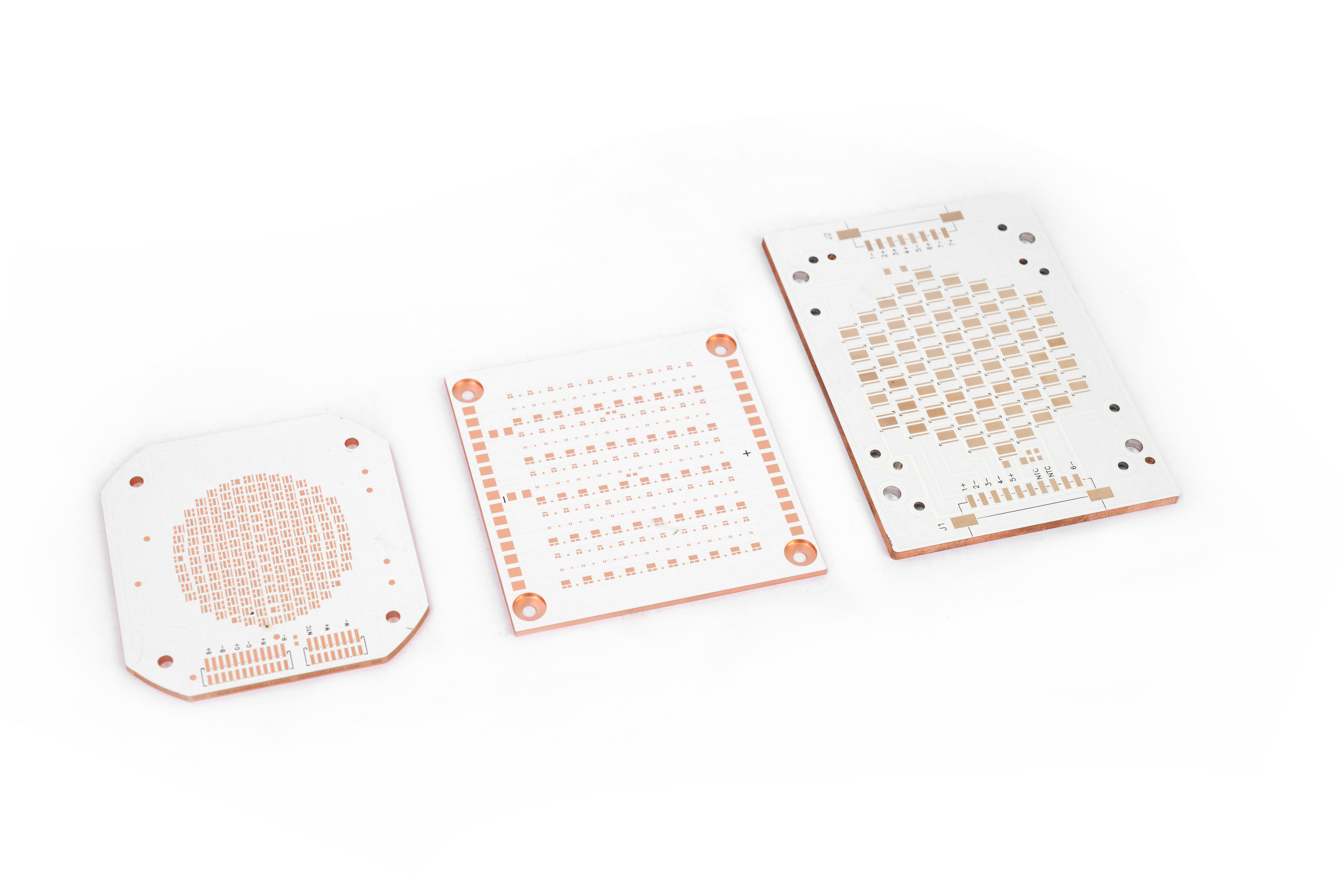
An aluminium core PCB, often called a metal core PCB, uses aluminium core PCB material as the main substrate layer. This layer replaces standard FR4 to provide stronger heat transfer. The aluminium material has a dielectric layer and a copper circuit layer bonded to it. This stack keeps components cooler and more reliable in high-power circuits. Compared to other materials, aluminium is affordable, strong, and great at moving heat away from sensitive parts.
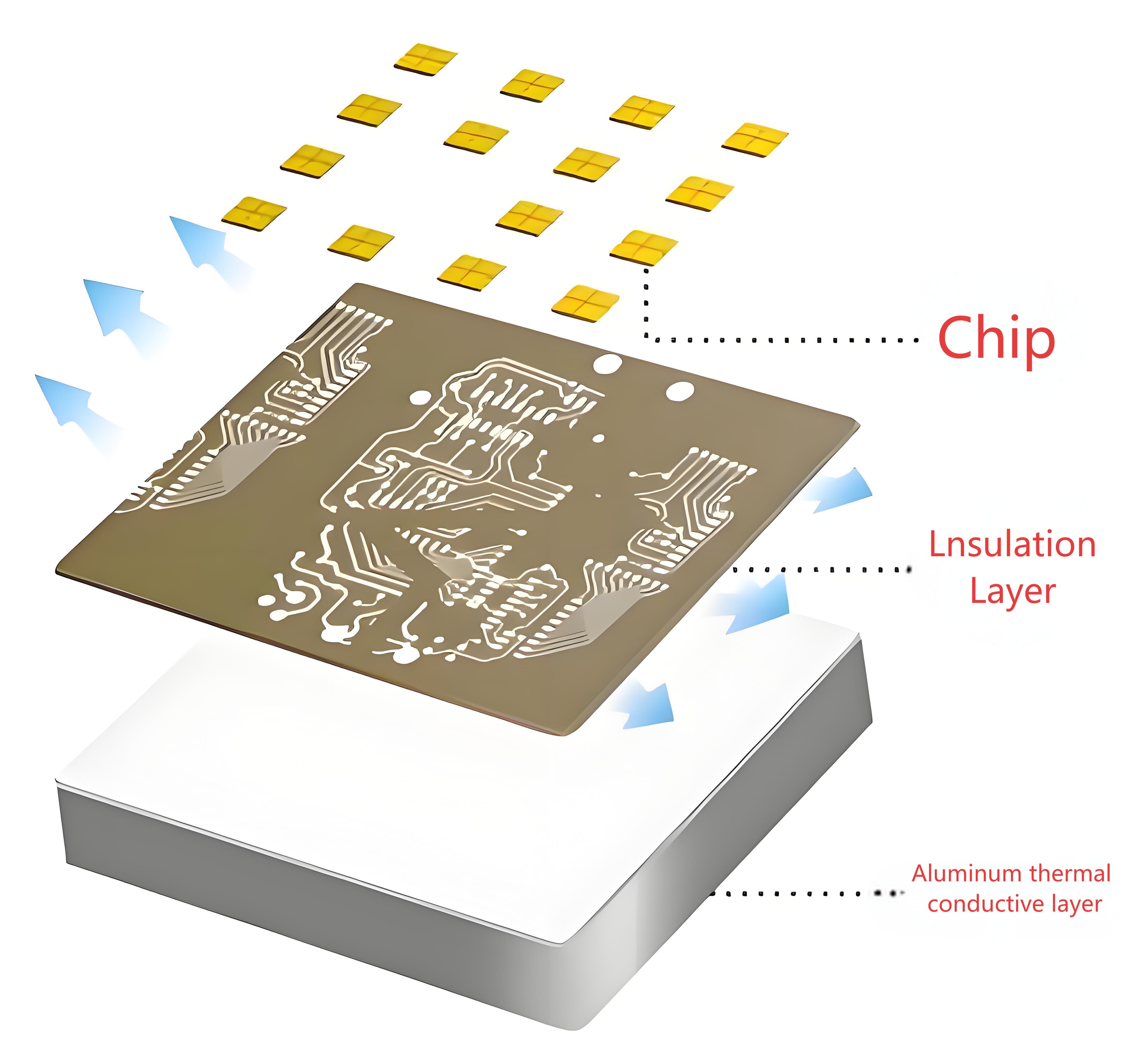
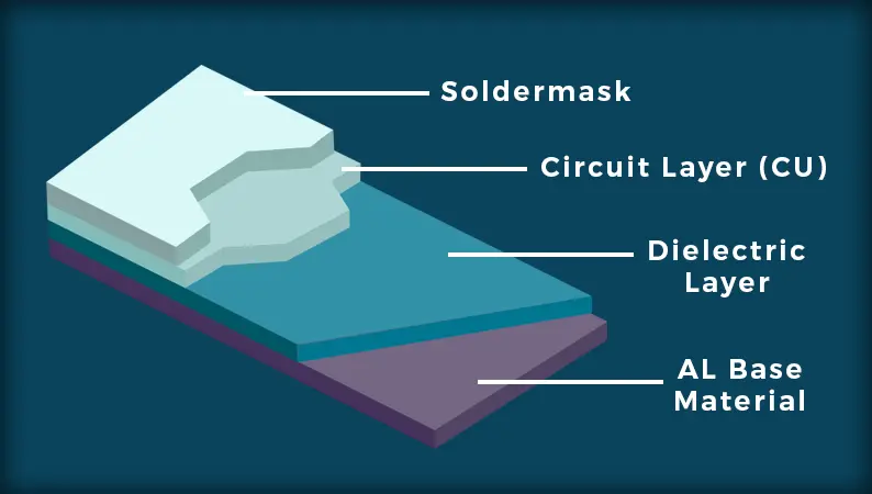
How is the Metal Core PCB Stackup?
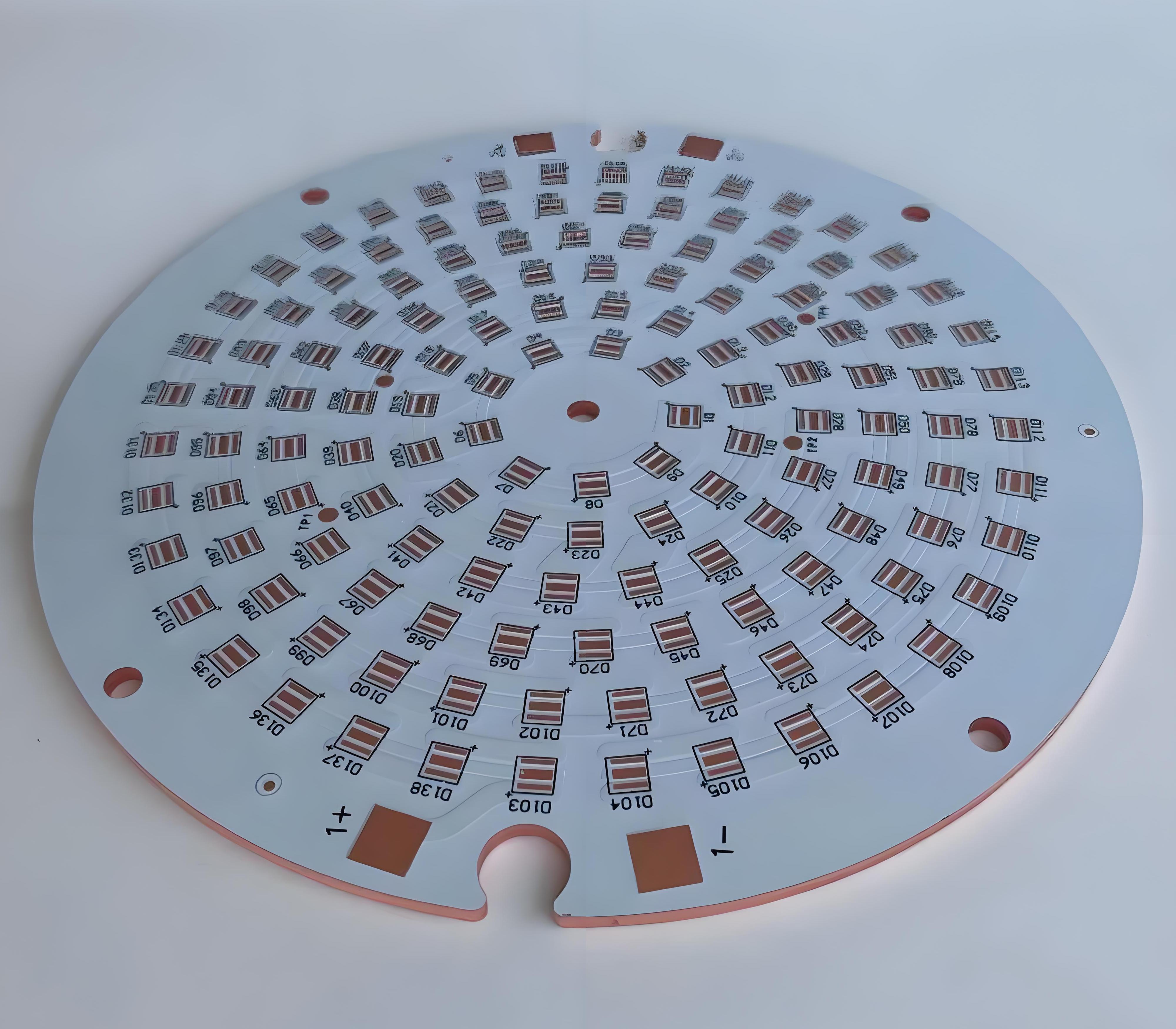
The metal core PCB stackup typically has three parts: the copper trace layer on top, a dielectric thermal insulation layer in the middle, and the metal base (usually aluminium) on the bottom. Some complex boards use multiple layers, but most LED and power PCBs use single-layer aluminium boards. The design focuses on directing heat through the dielectric into the core. This layout helps in high-brightness LED lighting and motor controls. It also improves stability in harsh environments.
What is the Difference: Alumina, Copper, and Aluminium Core PCB?
Aluminium core PCBs are different from copper or alumina ones in cost, weight, and thermal conductivity. Copper has higher thermal conductivity, but it is expensive and heavy. Alumina offers excellent insulation but is brittle and costly to process. Aluminium sits in the middle — affordable, light, and thermally efficient. That’s why many manufacturers choose it for mass production. It’s the perfect balance for most general power or LED uses.
| Feature | Alumina Core PCB | Copper Core PCB | Aluminium Core PCB |
|---|---|---|---|
| Category | Ceramic PCB | MCPCB | MCPCB |
| Thermal Conductivity | 15–35 W/m·K | 200–400 W/m·K | 1–5 W/m·K |
| Cost | High | Very High | Low |
| Weight | Medium | Heavy | Light |
| Mechanical Strength | Brittle | Strong | Moderate |
| Electrical Insulation | Excellent | Requires dielectric layer | Requires dielectric layer |
| Manufacturing Complexity | High (fragile material) | Moderate to High | Low |
| Common Applications | High-power RF, medical, aerospace | High-end power modules | LED lighting, automotive, power drivers |
What are the Advantages & Disadvantages: Aluminum PCB vs FR4?
When comparing Aluminum PCB vs FR4, each has clear strengths depending on the application. Aluminium PCBs perform better in thermal conditions, while FR4 is more flexible in multilayer layouts and low-cost builds. Here’s a side-by-side comparison:
| Feature | Aluminium PCB | FR4 PCB |
|---|---|---|
| Category | Metal Core PCB (MCPCB) | Standard Rigid PCB |
| Thermal Conductivity | 1–5 W/m·K (Good) | 0.2–0.3 W/m·K (Low) |
| Long-Term Reliability | High, stable under heat | Less stable at high temp |
| Mechanical Strength | High, resistant to shock | Medium, can deform |
| Thermal Expansion Match | Close to copper foil (24 ppm/°C) | Better expansion control than aluminium |
| Layer Flexibility | Limited to 1–2 layers | Supports multilayers (2–20+) |
| Design Flexibility | Low, not for dense designs | High, ideal for complex layouts |
| Cost | Higher | Lower |
| Weight | Heavier | Lighter |
| Common Uses | LED, power modules, automotive | Consumer electronics, mobile |
In conclusion, aluminium boards lead in heat performance and mechanical strength, making them ideal for power-heavy applications. On the other hand, FR4 remains more flexible for multilayer, compact, and cost-sensitive products. Choosing between them depends on your project needs.
Why is Aluminium Core PCB Used in Circuit Boards?
Aluminium core PCBs are widely used in modern electronics that demand high thermal efficiency and long-term reliability. Here are the main reasons:
- Excellent Heat Dissipation
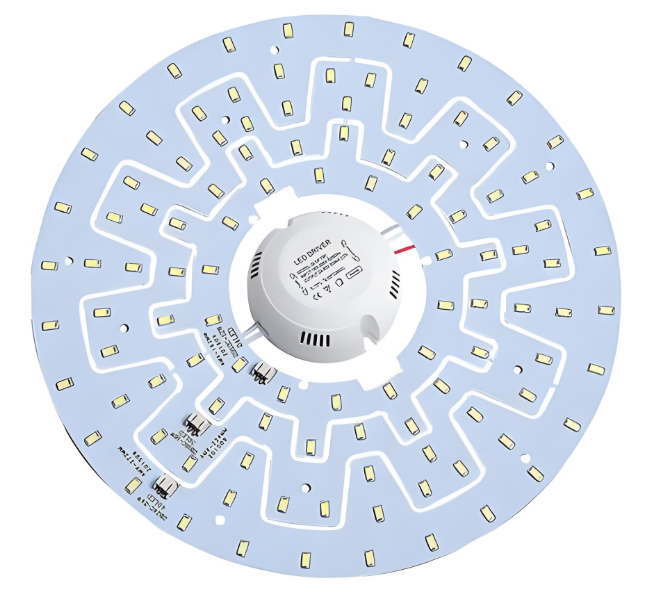
Aluminium core PCBs typically offer thermal conductivity between 1 to 5 W/m·K—far higher than standard FR4 boards. This helps to quickly transfer heat away from components, preventing performance drop or damage caused by overheating. It’s especially valuable in LED lighting, high-power circuits, and automotive control systems. - High Reliability Under Harsh Conditions
Thanks to their aluminum base, these boards withstand high temperatures and resist warping. They remain stable even in long-term use, which is why they’re often seen in outdoor lighting, power inverters, and industrial machines. - Enhanced Mechanical Strength
The aluminum core adds rigidity and impact resistance. This makes the PCB less likely to bend, crack, or break—ideal for applications that face mechanical stress or vibration. - Compact and High-Power Design Compatibility
Because aluminium PCBs can effectively handle heat in small spaces, they enable engineers to design smaller yet more powerful devices. This is critical for compact modules in LED drivers, medical equipment, and telecom hardware. - Improved Signal Integrity
By maintaining thermal balance and structural stability, aluminium PCBs reduce the risk of thermal expansion mismatches and signal interference. This helps ensure consistent performance in high-frequency and high-speed circuits.
What is the Aluminium PCB Manufacturing Process?
- Base Material Preparation
The process begins with an aluminium substrate laminated with a dielectric layer and copper foil. The dielectric ensures insulation and thermal transfer. - Dry Film Application & Imaging
A dry film is applied over the copper. UV exposure hardens the film according to the circuit pattern, followed by developing to reveal the copper to be etched. - Etching the Copper Layer
Chemical etching removes the unwanted copper, leaving behind the desired trace pattern on the aluminium core board. - Resist Stripping
The remaining dry film is stripped away, exposing the clean copper circuitry. - Drilling & Mechanical Processing
CNC drilling machines create holes for vias and mounting. EBest Circuit (Best Technology) uses precision drilling to meet tight tolerance demands. - Hole Cleaning & PTH Plating
The drilled holes are cleaned and then plated with copper to form conductive pathways between layers (if needed). - Solder Mask Application
A solder mask is printed onto the board to protect the traces and prevent solder bridging during assembly. - Surface Finishing
The exposed copper pads receive surface finishes such as ENIG or OSP to improve solderability and prevent oxidation. - Profiling / Routing
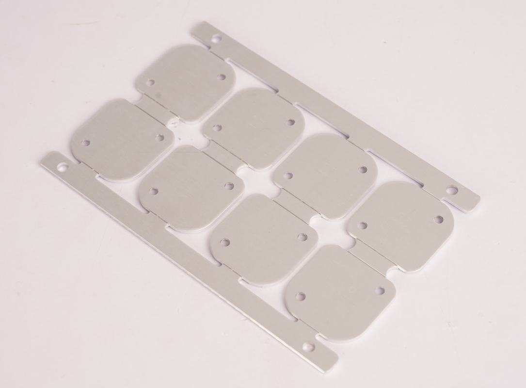
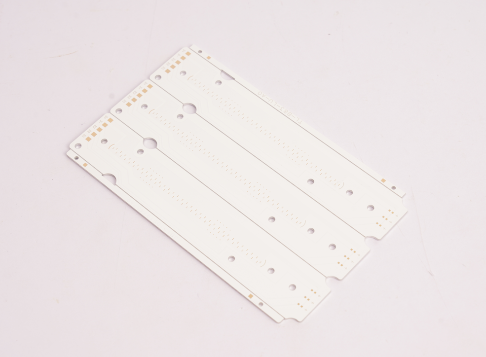
CNC equipment cuts the finished boards into the desired shapes, ensuring sharp edges and consistent outlines. - Electrical Testing
Every aluminium PCB is tested using Flying Probe or E-test systems. EBest Circuit (Best Technology) also utilizes AOI to catch early-stage defects. - Final Cleaning & Inspection
The boards are thoroughly cleaned and inspected. MES traceability links each board to its production record, ensuring consistent quality and easy tracking.
How is the Aluminium Core PCB Price?
The aluminium core PCB price depends on factors like board size, thickness, copper weight, and layer count. Simple single-sided LED boards are cheaper, while high-power double-sided boards cost more. Overall, aluminium is cheaper than copper and more effective than FR4 in heat-sensitive applications. EBest Circuit (Best Technology) offers fast delivery services, especially for bulk orders, while maintaining high-quality standards. Our 19 years of rich experience and responsive sales team also help reduce processing time for your project.
Why Choose EBest Circuit (Best Technology) as One of Your Trustworthy Aluminium Core PCB Manufacturers?
As one of the leading aluminium core PCB manufacturers, EBest Circuit (Best Technology) offers more than just fabrication. We help clients with design advice, fast prototyping, and complete assembly services. Many customers face problems like poor thermal contact, unstable performance, or long delivery cycles. We solve these by:
- Using high-grade aluminium PCB board for LED lighting and industrial applications
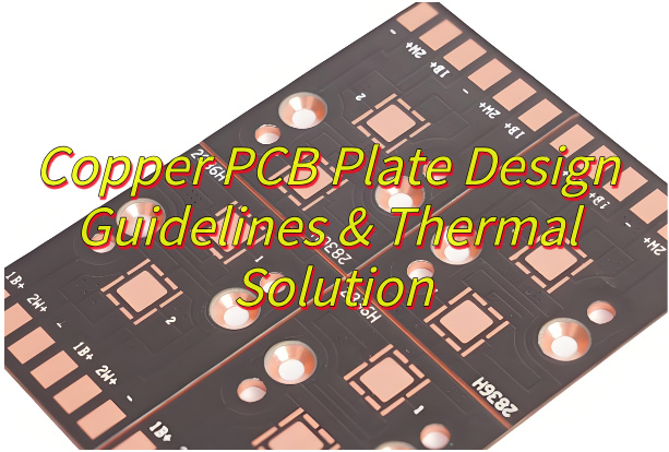
- Following metal core PCB design guidelines to reduce overheating risks
- Applying DFM reviews to prevent layout mistakes and production delays
- Providing IPC Class 2 & 3 standards for reliable operation
- Customizing stackups and finishes to fit your exact needs
- Processing prototype, high volume metal core PCB manufacturing and SMT process under one roof, without PCB contracting to other suppliers.
Our edge also lies in fast delivery. Some customers had to wait weeks for prototypes elsewhere. We reduce that to days, thanks to in-house CAM engineers and flexible production lines. You can also trust our team to provide prompt updates and solid advice throughout the order. That’s why many top-tier clients stick with EBest Circuit (Best Technology) for years.
To sum up, aluminium core PCBs make thermal problems easier to solve. Whether you’re building LED lighting, motor controllers, or power converters, these boards support better heat flow and stability. The balance of cost, performance, and ease of manufacturing makes them a smart choice. With clear benefits over FR4 and a simpler process than copper or alumina, aluminium PCBs are here to stay.
At EBest Circuit (Best Technology), we bring deep expertise, quick response, and complete support from design to assembly. We also understand customer headaches like unstable sourcing, low product yield, or miscommunication during prototyping. That’s why we built our customer policy: customer first and maintain quality consistency. We invite you to send us an email about what MCPCB you need or what your project headaches are. Then we’ll feature our metal core PCB portfolio and let you know our Aluminium core PCB price correspondingly. Here is our contact email: sales@bestpcbs.com.