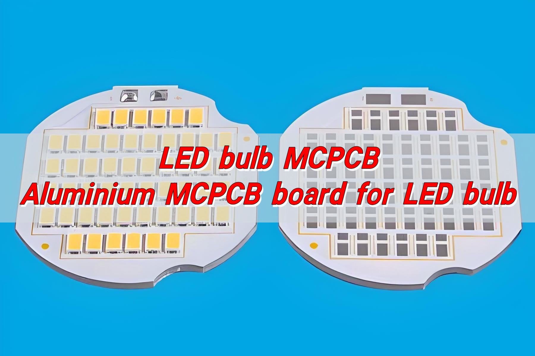
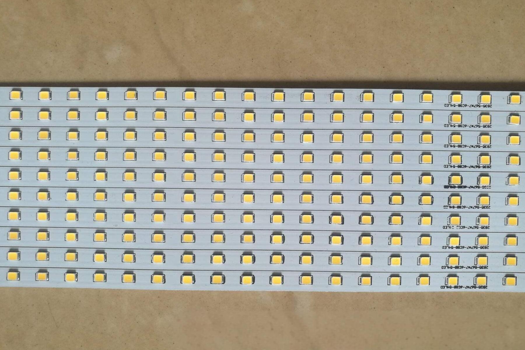
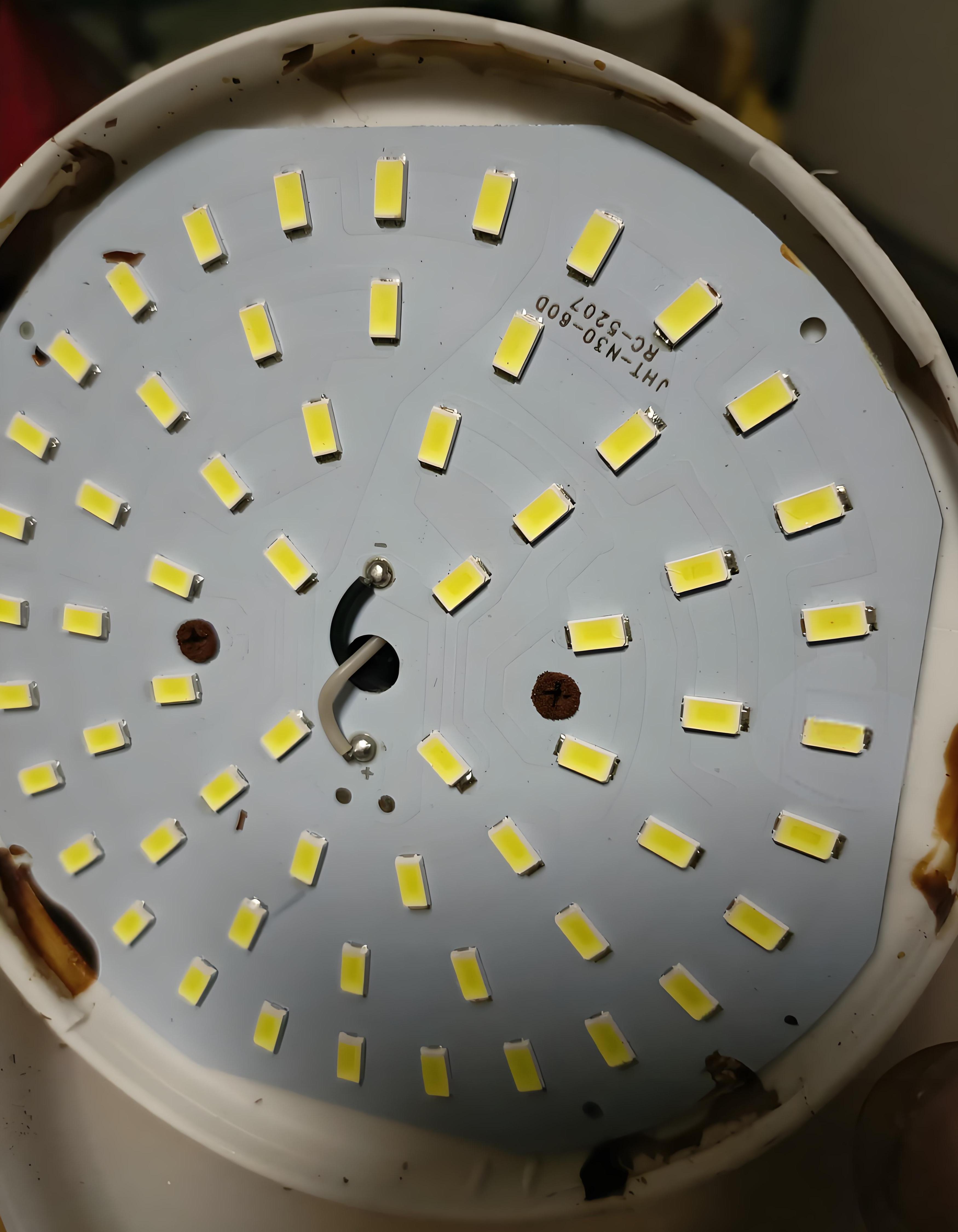
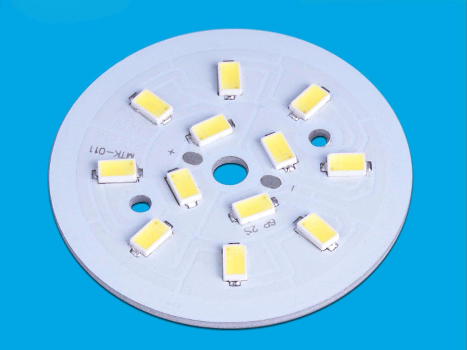
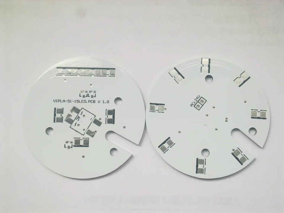
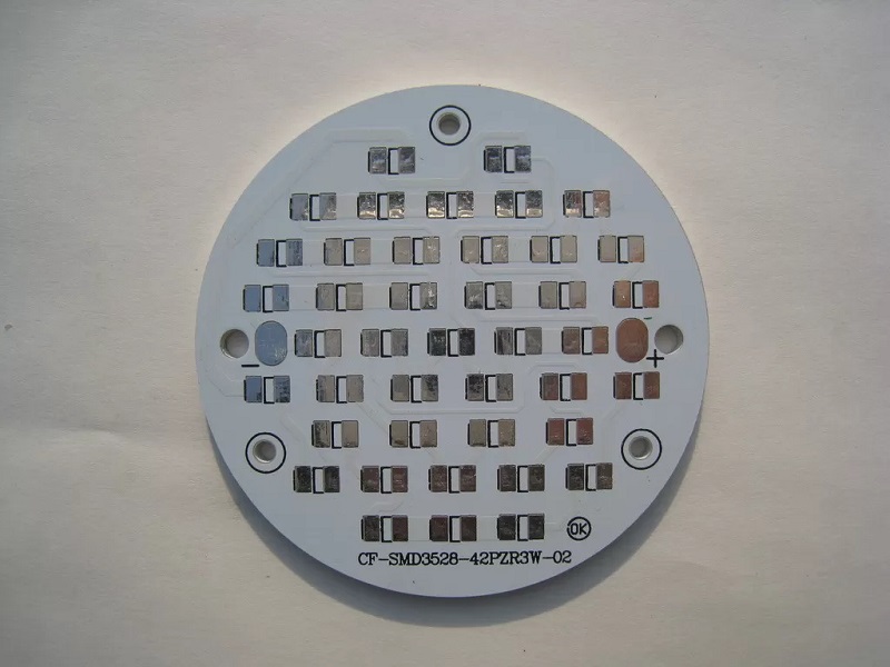
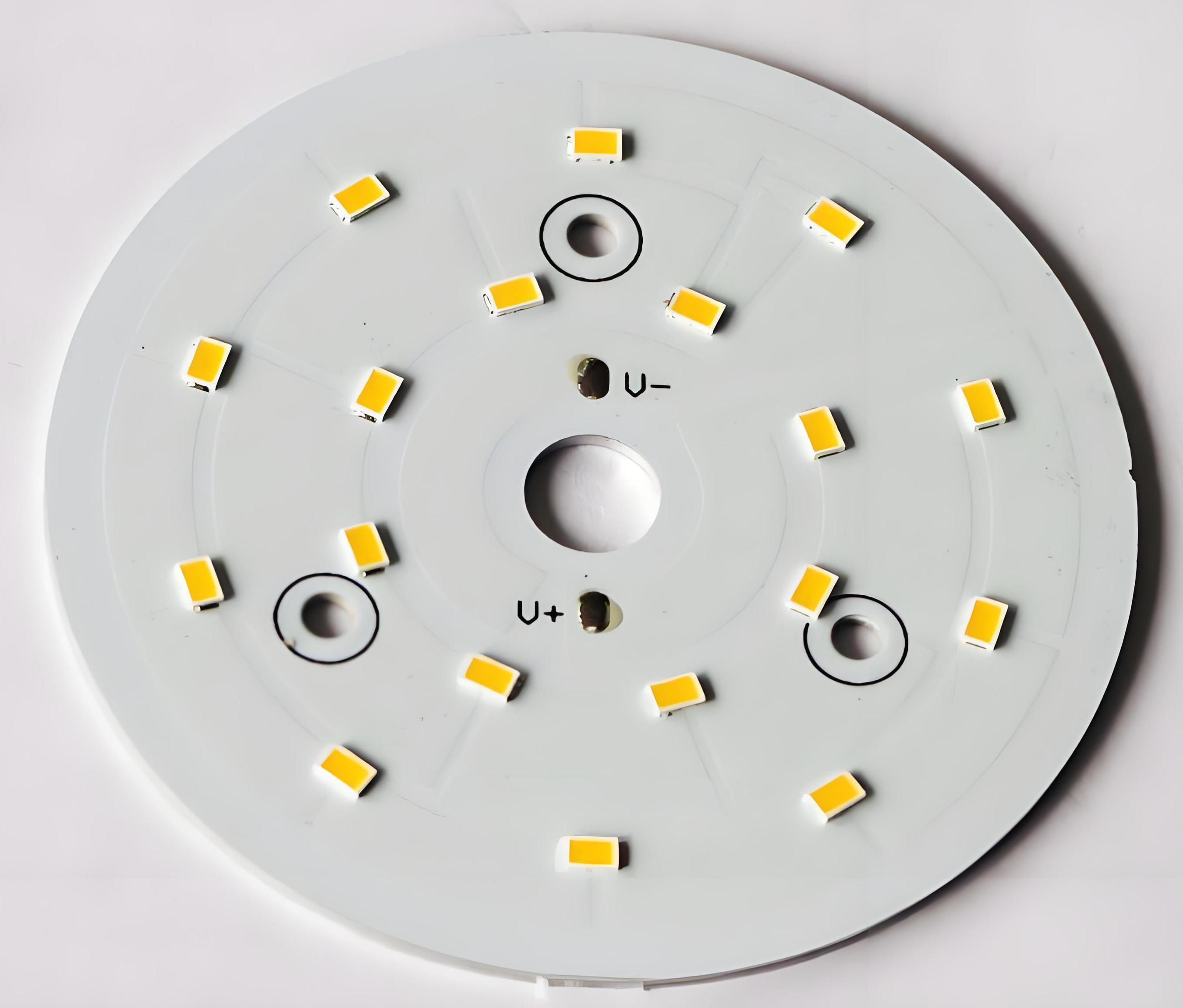
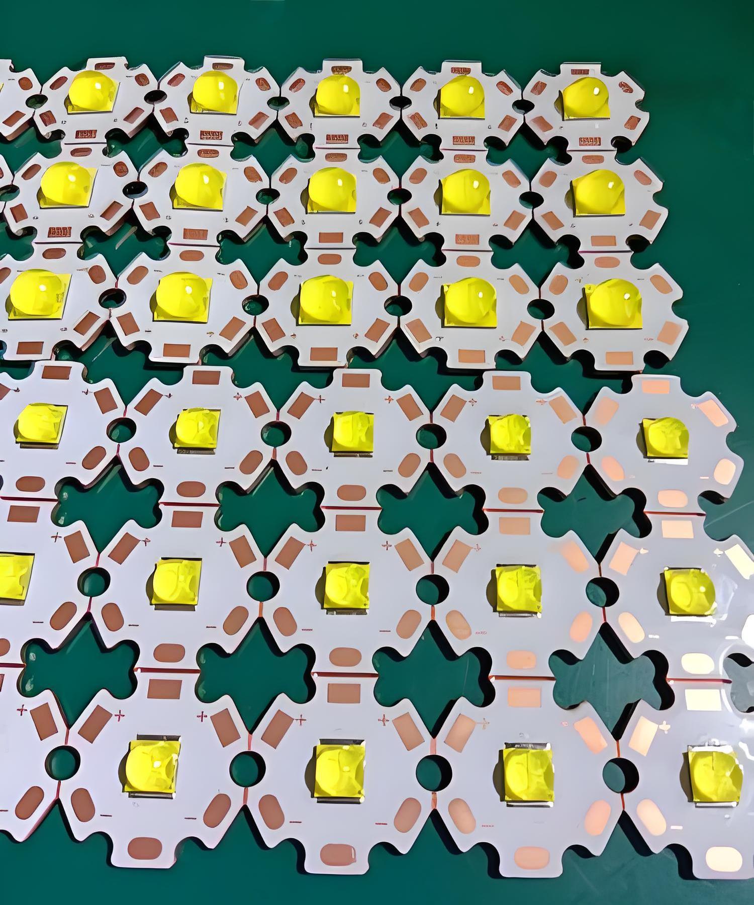
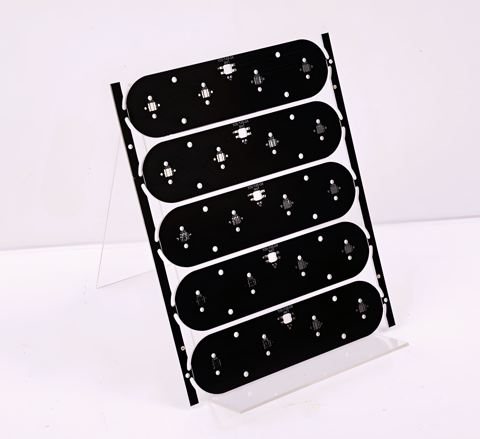
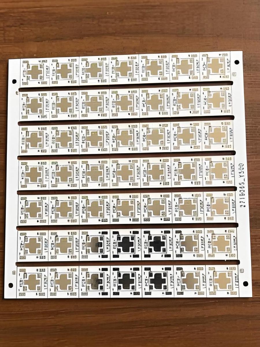
Aluminium core PCB is a printed circuit board that uses aluminum as its base layer. It’s designed to transfer heat away from components quickly, keeping devices cool and stable. This makes it ideal for high-power applications like LED lighting, automotive systems, and power electronics.

What is metal core pcb?
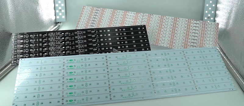
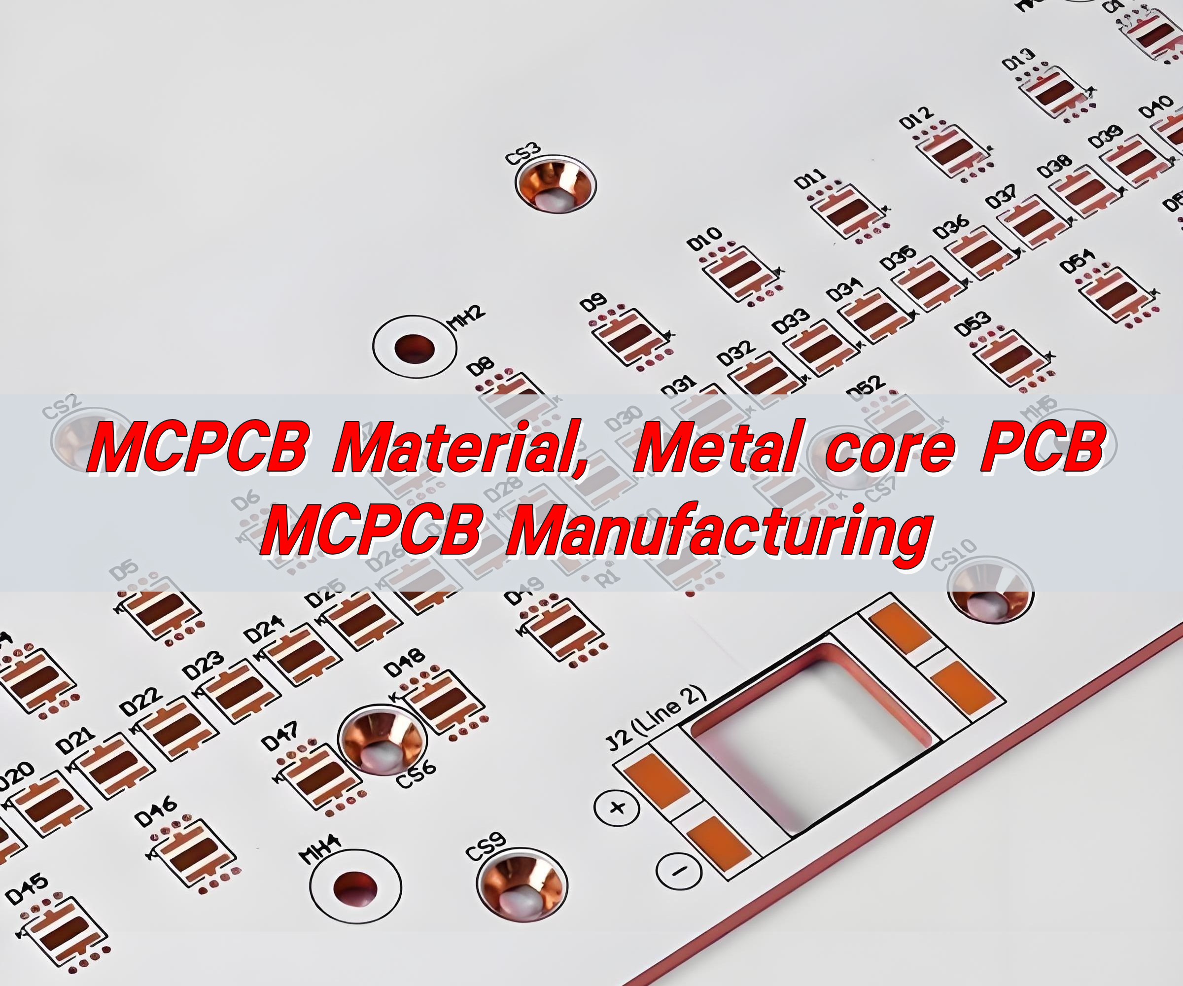
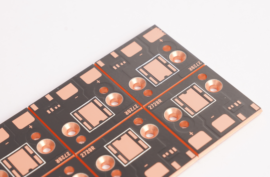
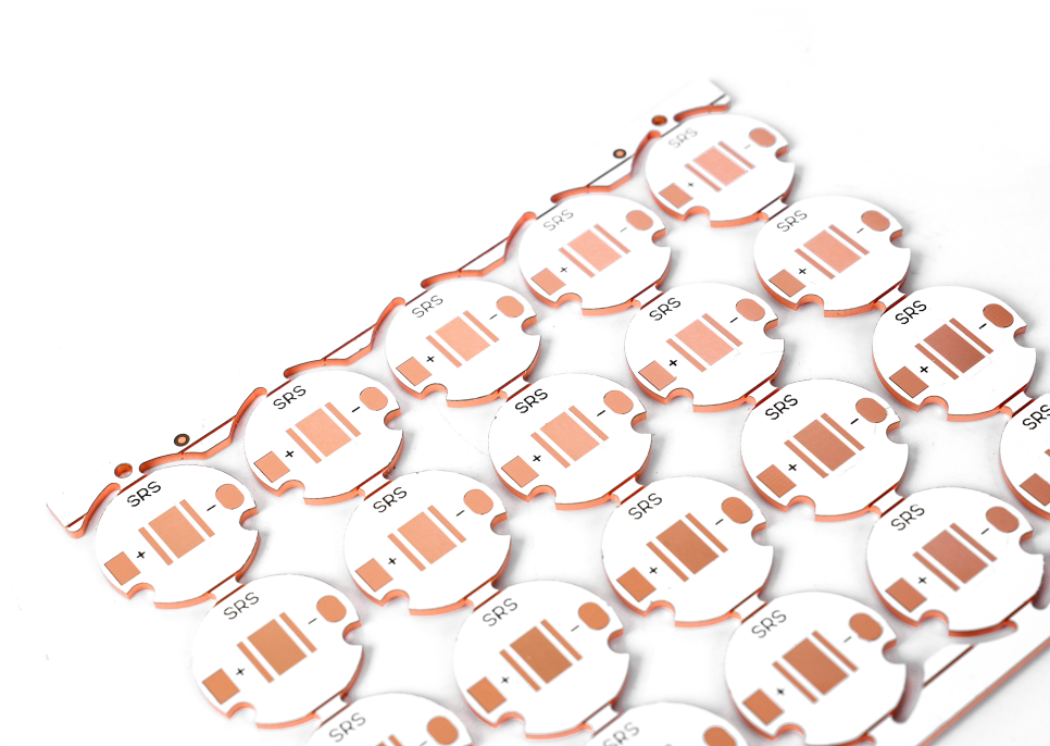
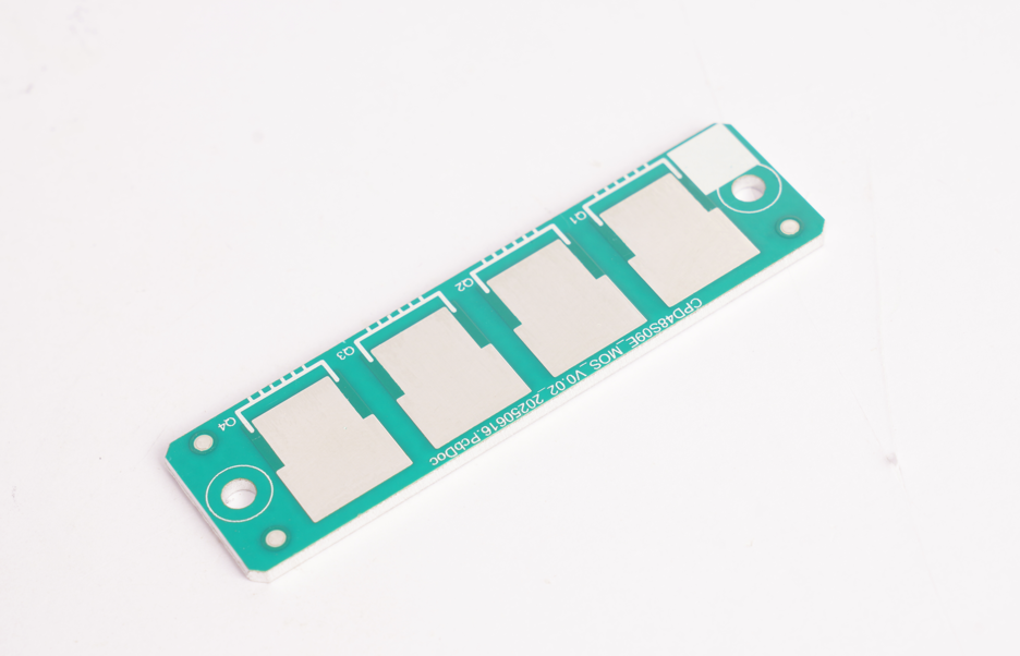
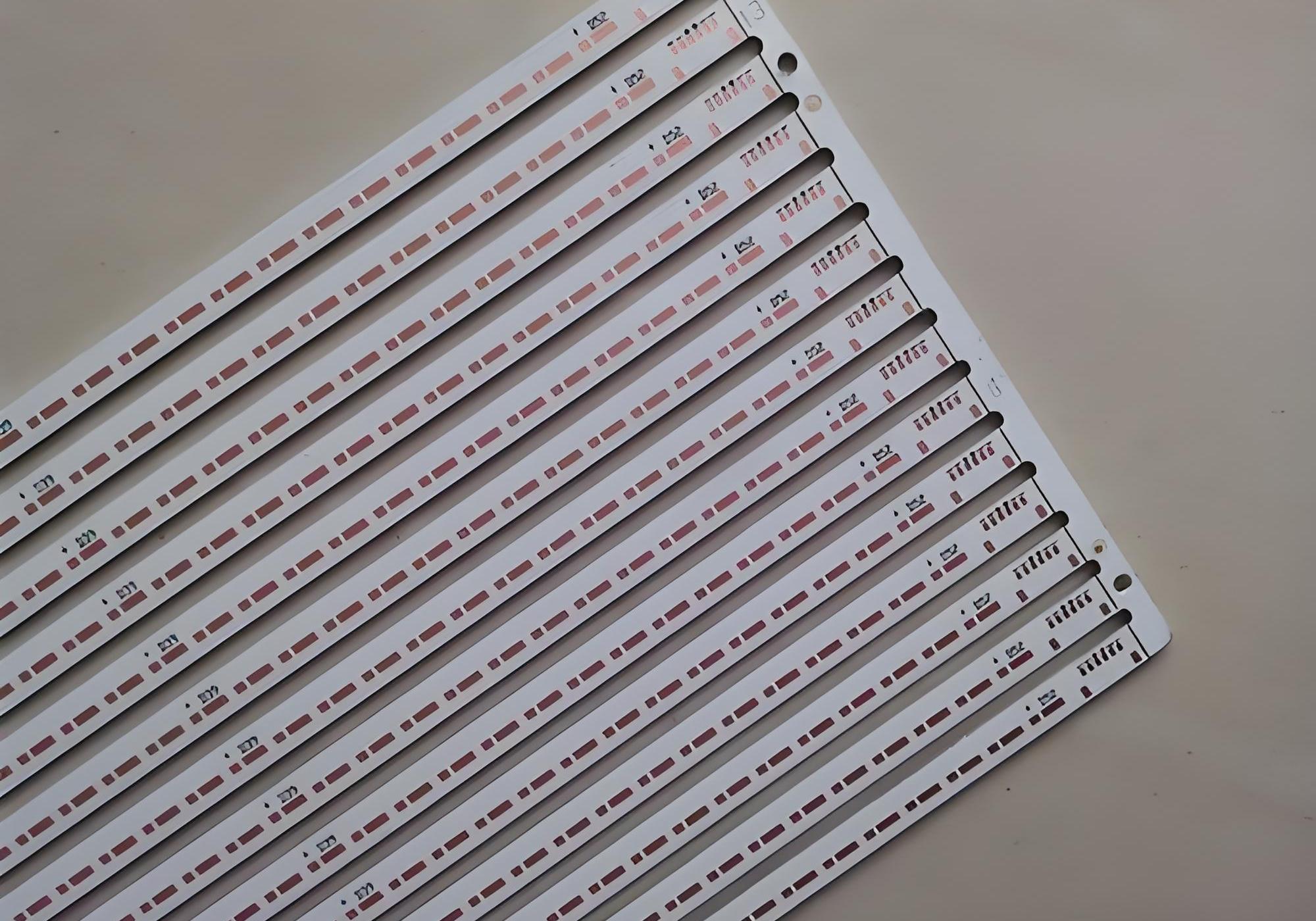
Metal core PCB, often called MCPCB, uses a metal base instead of the traditional FR4 or epoxy glass. This base is usually aluminium, copper, or a mix of both. Among them, aluminium metal core PCBs are by far the most popular due to their balance of performance, weight, and cost.
This core serves as the backbone of the PCB, offering strong thermal conductivity, mechanical support, and efficient heat dissipation. These properties make it ideal for high-power circuits where temperature control is critical.
Why use a metal core PCB?
Electronic components, especially high-power LEDs and MOSFETs, generate heat. If that heat stays trapped, it kills performance and shortens lifespan.
Metal core PCB fights this issue head-on. Its design allows heat to transfer quickly from the circuit layer to the metal base, keeping components cool and stable. That means fewer failures, longer device life, and lower maintenance.
They’re not just about heat. MCPCBs also improve structural strength, reduce size, and support higher component density. All these benefits combined make them a go-to for industries like automotive, telecommunication, aerospace, and medical devices.
What are the pros and cons of aluminum PCB?
Every material has its strengths and weaknesses. But in the case of aluminium PCBs, the pros are far more impressive than the cons.
Advantages:
- Excellent Thermal Management: Aluminium pulls heat away from hot components, preventing damage.
- Lightweight Yet Strong: Compared to copper, aluminium offers solid durability at a lower weight.
- Cost-Effective: It’s more affordable than copper but delivers reliable thermal conductivity.
- Eco-Friendly: Aluminium is recyclable and non-toxic, helping meet sustainability goals.
- Improved Dimensional Stability: The structure remains stable even under changing temperatures.
Disadvantages (Very Few):
- Slightly less flexible than FR4 in design.
- Electrical insulation must be carefully managed to avoid short circuits.
Still, for most applications, these drawbacks are easily handled by professional manufacturers.
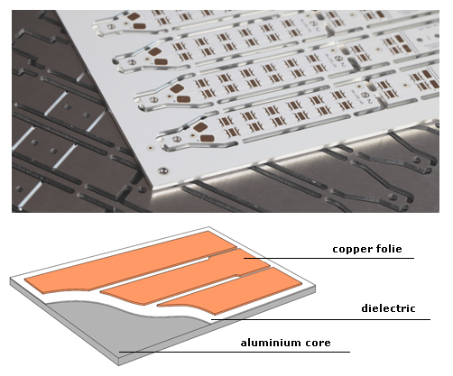
What does aluminum core mean?
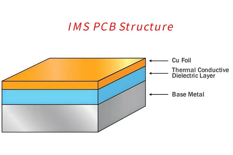
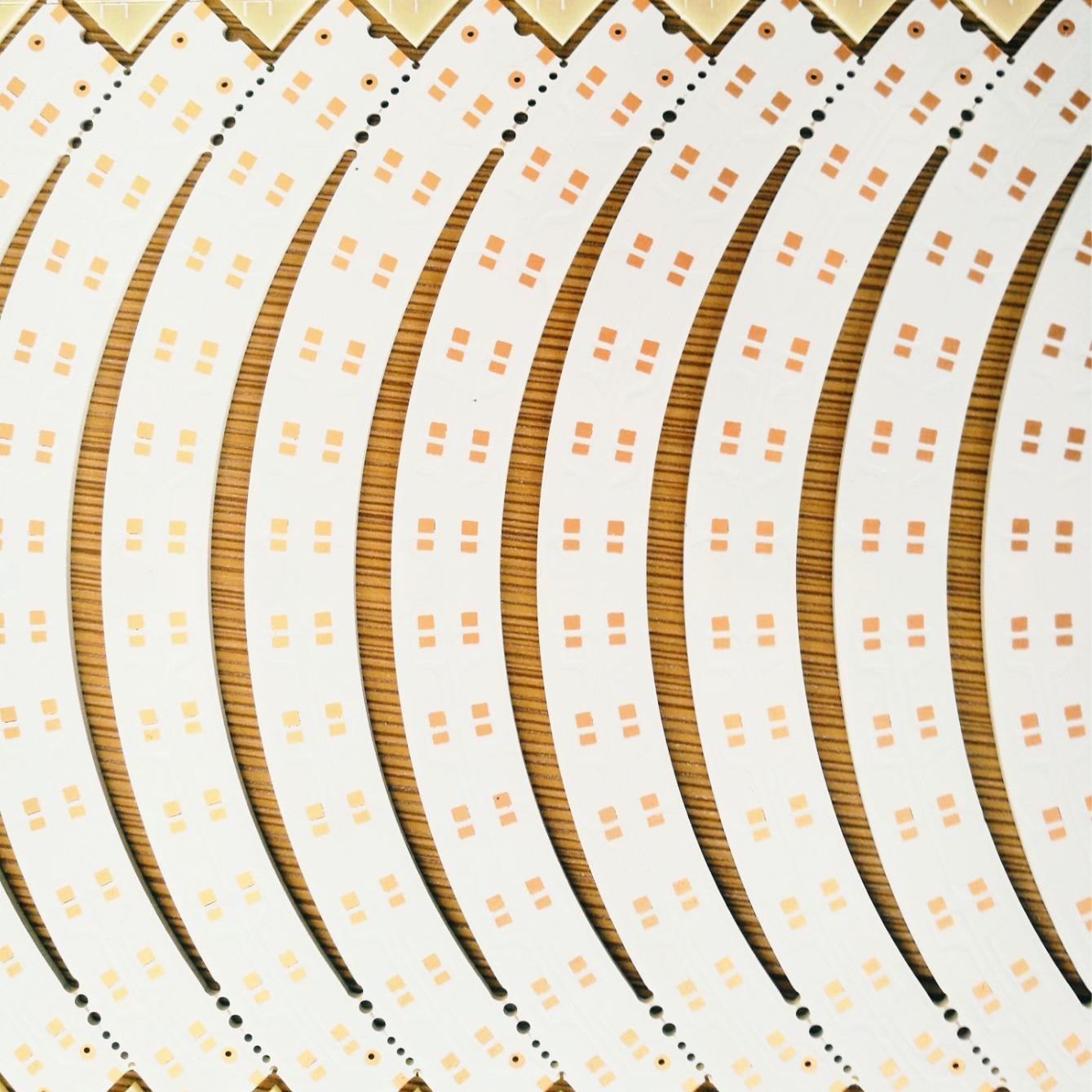
Aluminum core PCB refers to a circuit board with three main layers:
- Copper Circuit Laye: This is where your electronic components sit.
- Dielectric Layer: An insulating layer that transfers heat to the core while isolating electricity.
- Aluminium Base Layer: A thick base of aluminium that provides strength and heat sinking.
This core turns a standard PCB into a high-performance solution, especially for high-current and high-heat devices.
Why choose an aluminum core PCB?
There are many reasons to choose aluminum core PCB instead of traditional PCB. Its core advantages go far beyond temperature control. Here’s why they shine:
- Superior Heat Dissipation: Keep components safe even in the most demanding power applications.
- Durable Construction: Withstands mechanical stress and harsh environments.
- Compact Design: Allows for smaller, thinner devices without sacrificing reliability.
- Better Reliability: Lowers the risk of overheating, which often causes circuit failure.
- Improved Energy Efficiency: Less heat means less energy wasted, which is a win in power-sensitive applications.
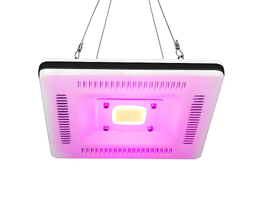
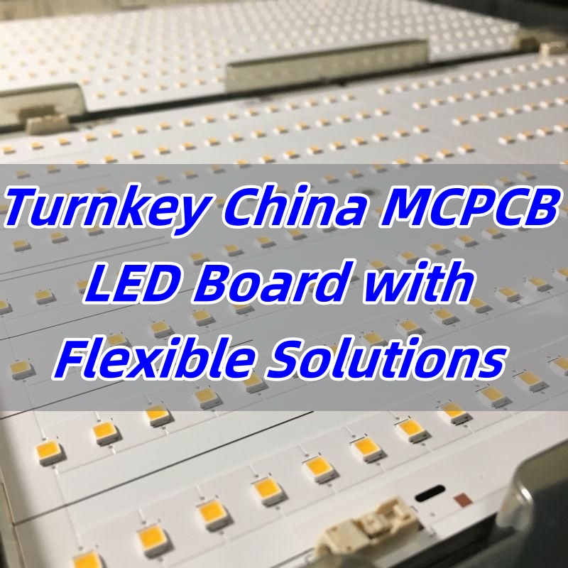
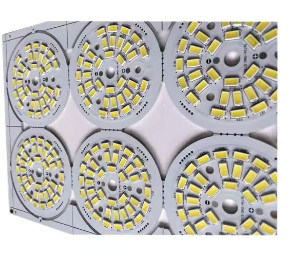
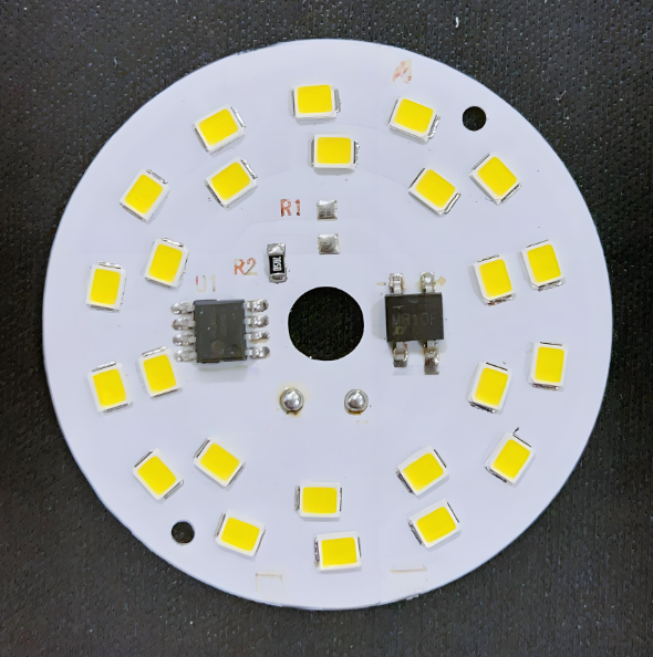
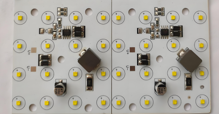
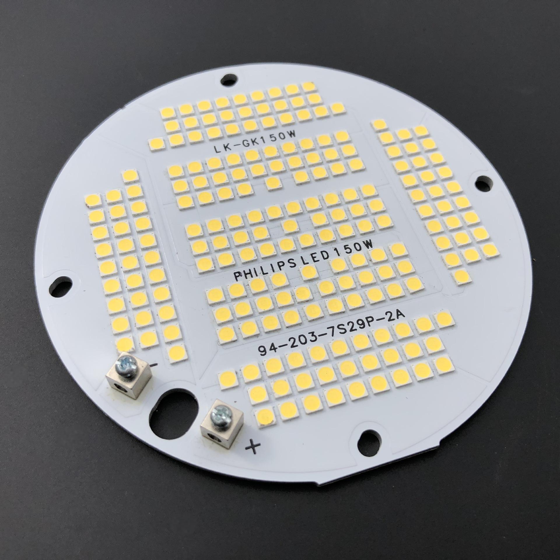
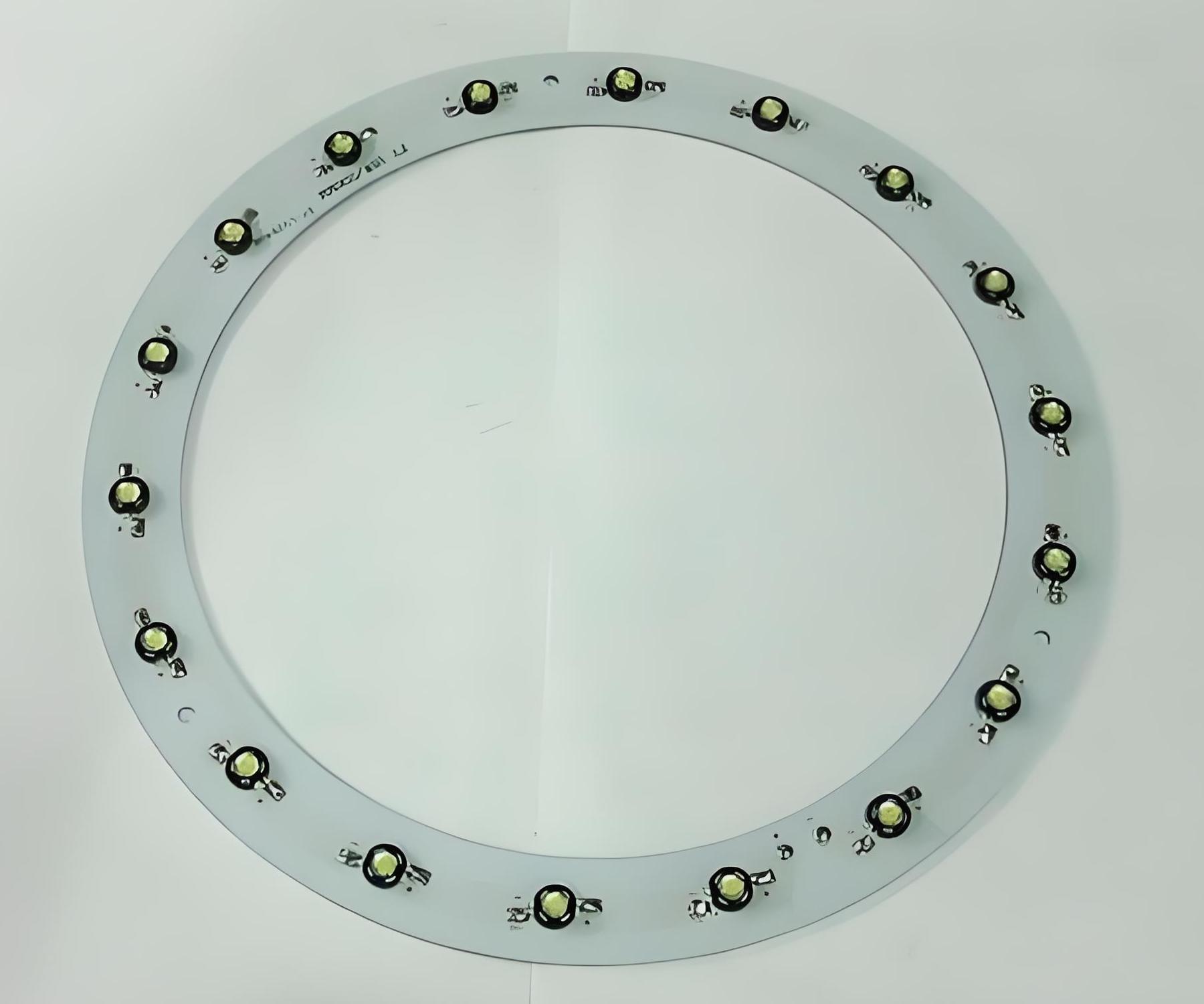
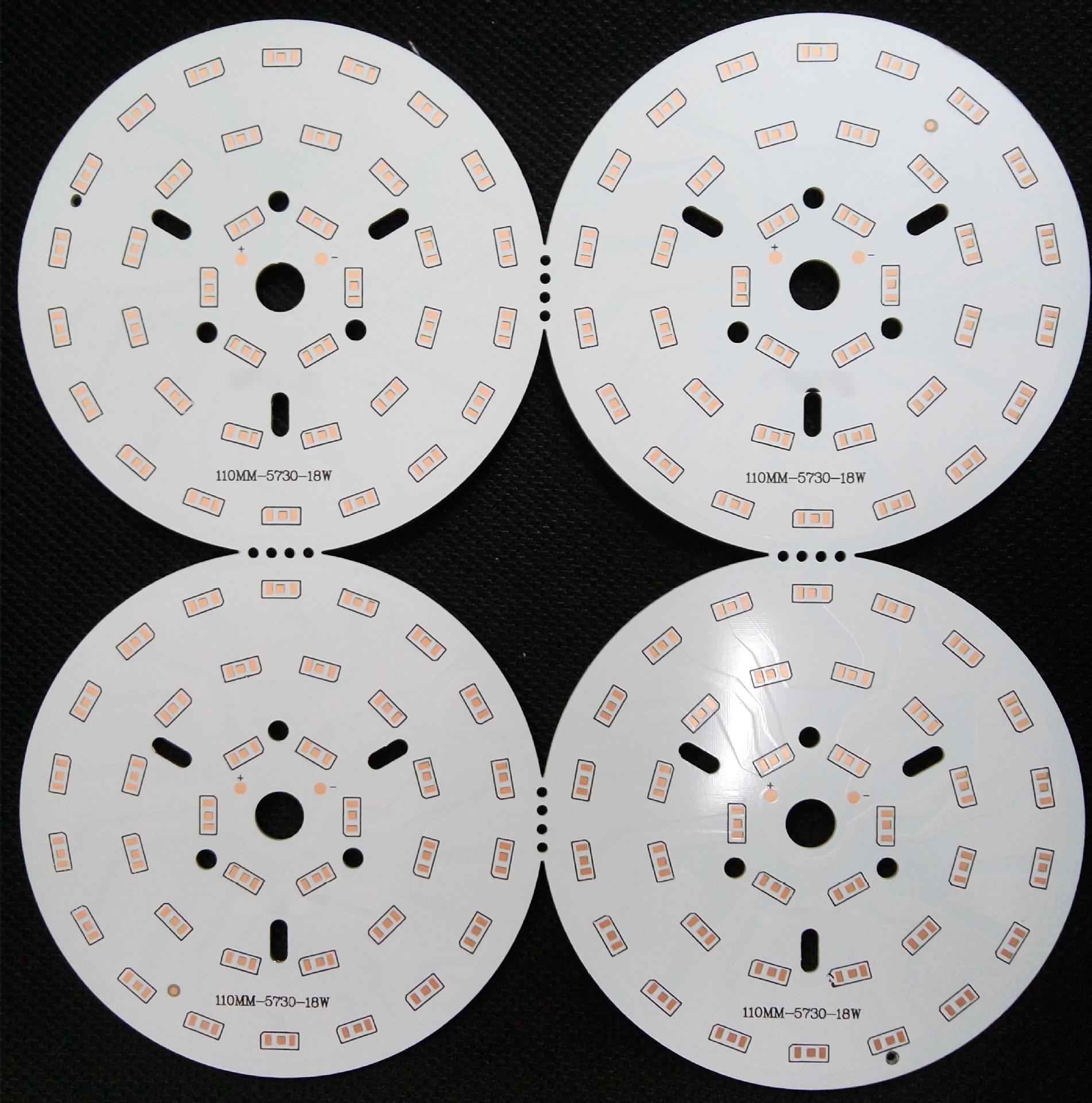
- Great for LED Applications: Aluminium PCBs have become the backbone of LED lights due to their excellent thermal properties.
If your end product needs to perform well under pressure, aluminium core PCBs are a rock-solid choice.
How is aluminium PCB made?
The aluminium PCB manufacturing process is both precise and efficient. Here is a brief process of the aluminum substrate PCB factory:
- Raw Material Preparation – Aluminium base is selected, cleaned, and pre-treated for bonding.
- Dielectric Layer Application – An insulating, thermally conductive layer is laminated onto the aluminium.
- Copper Cladding – A copper sheet is bonded on top of the dielectric.
- Image Transfer – Circuit patterns are printed and developed on the copper layer.
- Etching – Unwanted copper is removed, leaving the circuit behind.
- Solder Mask and Silkscreen – Protective coatings and labels are added.
- Surface Finish – Finishing like ENIG, HASL, or OSP is applied to improve solderability.
- Testing – Electrical and visual inspections are done to ensure perfection.
BEST Technology’s modern factory uses automated production lines and strict quality control to produce high-reliability circuit boards at competitive aluminum plate prices.
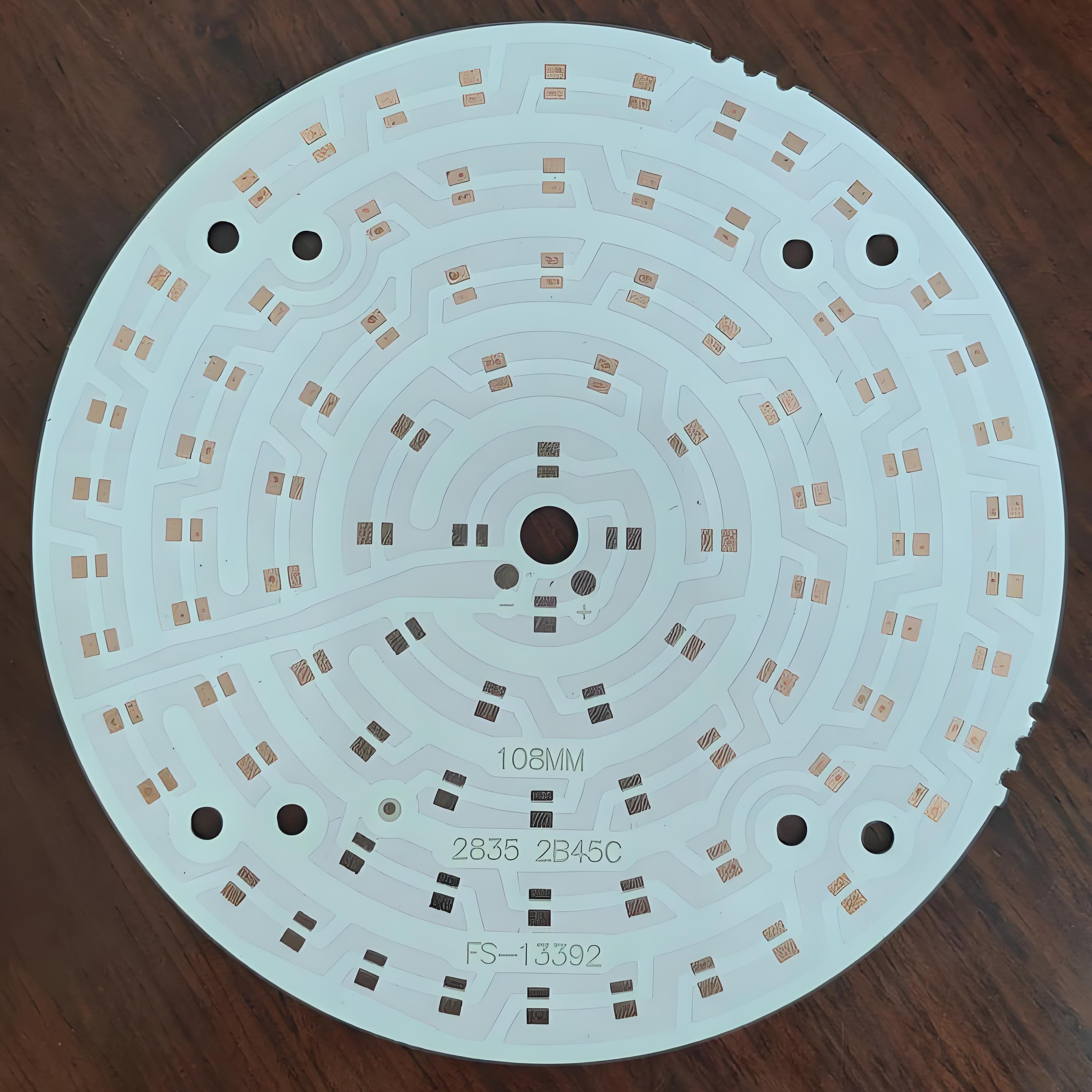
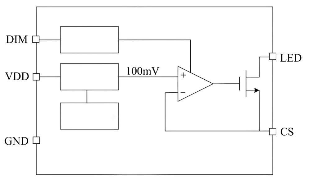
How does PCB stackup affect heat?
The layer structure of a PCB controls how well it dissipates heat and shields signals. For aluminium metal core PCBs, the stackup typically follows this pattern:
- Copper layer on top for components
- Thin dielectric for thermal transfer
- Thick aluminium base for heat sinking
This simplified layout boosts thermal flow. By reducing the thermal resistance between heat-generating components and the aluminium base, the heat escapes more efficiently.
A good PCB stackup design ensures low heat buildup, better EMI performance, and long-term reliability.
What is the difference between aluminum PCB and FR4?
FR4 PCBs use fiberglass-reinforced epoxy as the core. They’re cheap, widely used, and fine for low-power electronics. But they trap heat. When used in high-power circuits, the temperature rise can damage components.
Aluminum PCBs, on the other hand, replace the FR4 core with a metal core. This major change improves:
- Heat transfer
- Mechanical strength
- Lifespan
- Power capacity
Also, FR4 lacks the ability to dissipate heat efficiently, while aluminium PCBs can handle up to 10× better thermal flow. That’s why they dominate in LED lighting, automotive modules, and industrial drives.
What’s the thermal conductivity of aluminium core PCB?
The thermal conductivity of an aluminium core PCB depends on the dielectric layer and aluminium grade, but it usually ranges between 1.0 W/mK to 3.0 W/mK. Some high-end materials can reach up to 5.0 W/mK.
By comparison, FR4’s thermal conductivity is just 0.25 W/mK. That makes aluminium core PCBs around 4 to 20 times more effective at transferring heat.
Conclusion:
Aluminium core PCBs offer powerful thermal management, high durability, and compact design, making them ideal for modern electronics like LED lighting, power supplies, and automotive systems. Compared to traditional FR4 boards, they handle heat far more efficiently, ensuring longer device life and better performance.
Need a reliable aluminium core PCB manufacturer? Contact us at sales@bestpcbs.com