What is MCPCB LED plate? This guide explores its construction, applications, design principles, manufacturing, and cost factors for optimal thermal management solutions.
Are you worried about these problems?
- Does your lamp lose 30% brightness after half a year of use?
- Is the chip scrapped due to deformation of the substrate?
- Does the micro-pitch LED below P1.0 have local overheating due to insufficient heat dissipation?
EBest Circuit (Best Technology) can provide solutions:
- 1.2W/m·K high thermal conductivity aluminum substrate + 5mil ceramic insulation layer, junction temperature reduced by 18℃, actual measured data, free thermal imaging testing service.
- Pre-oxidation aluminum substrate (CTE16ppm/℃) ±0.08mm laser cutting process, 200+ customers verified 99% yield.
- Nano-ceramic coating technology (thermal resistance <1.0K·cm²/W), supports 0.5mm pad spacing design, has passed 10,000 hours accelerated aging test.
Welcome to contact us if you have any request for metal core PCB: sales@bestpcbs.com.
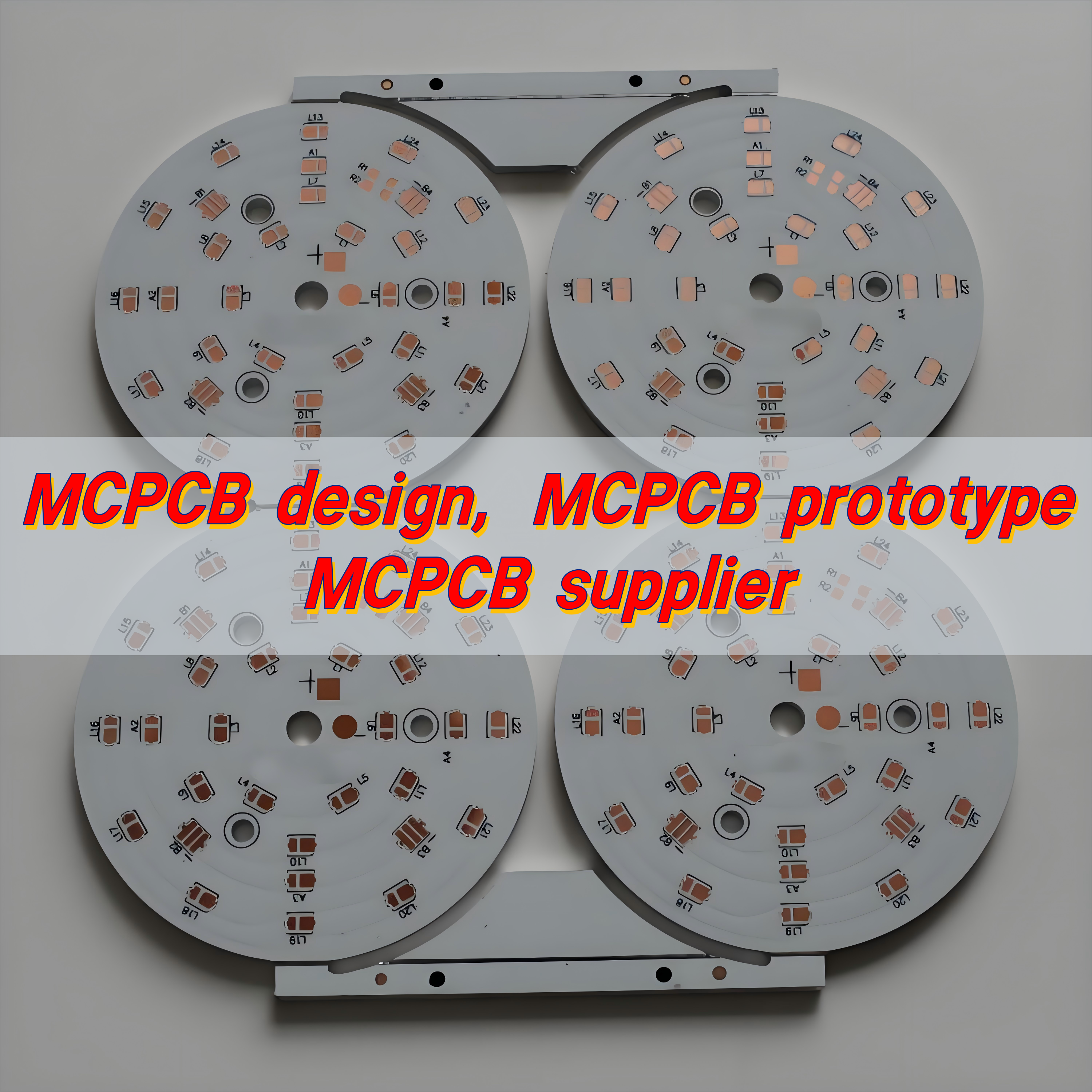
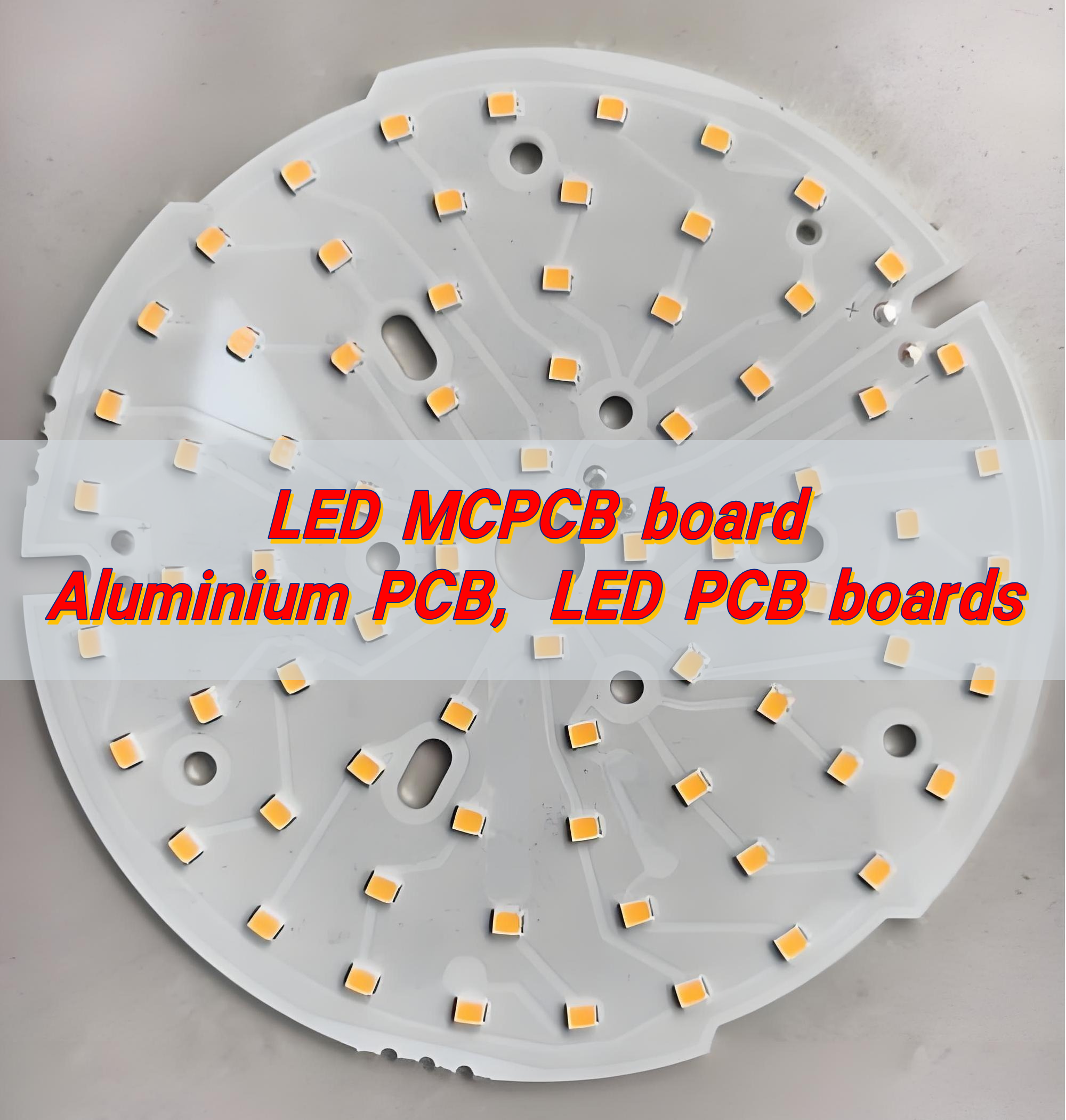
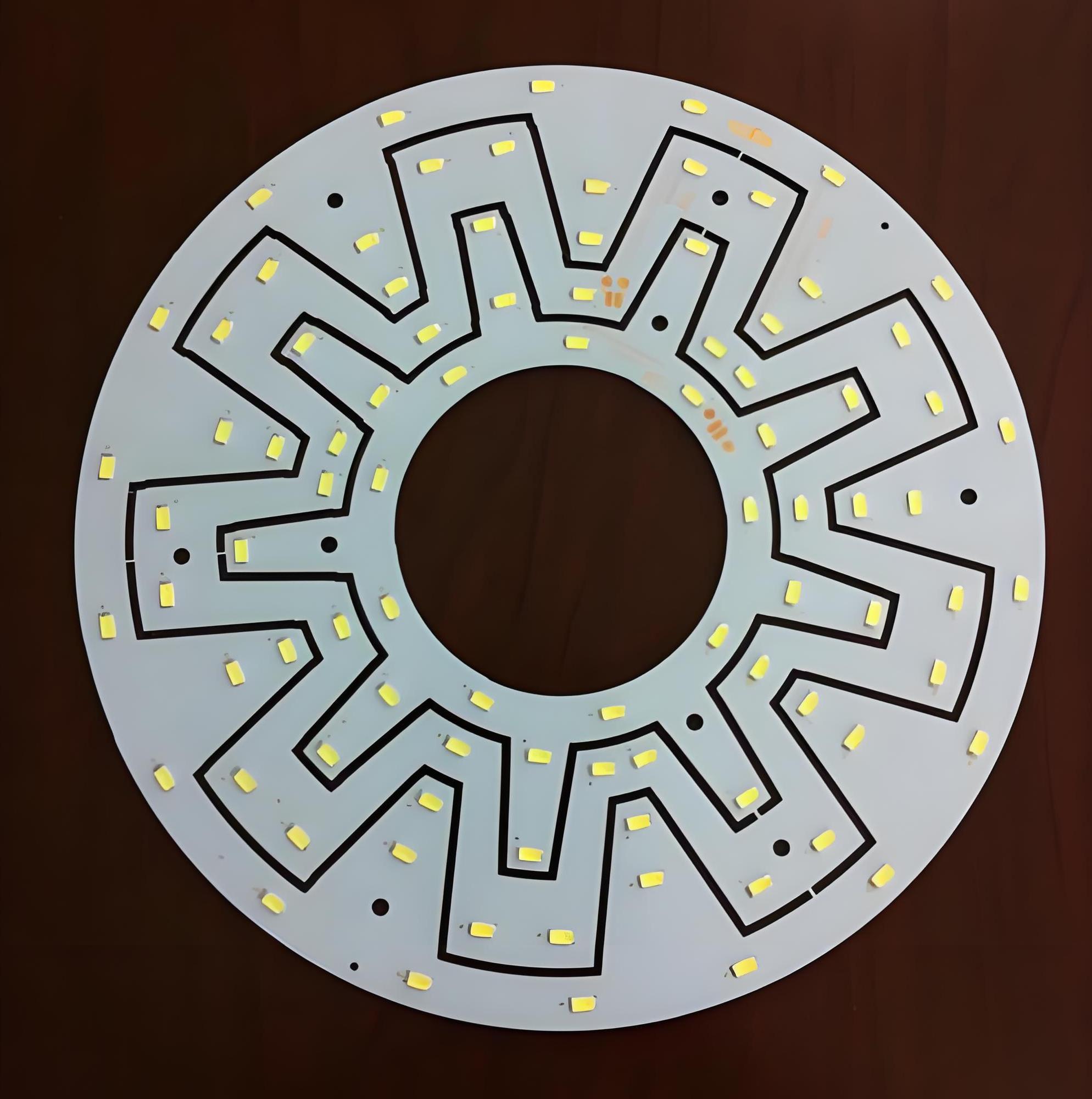
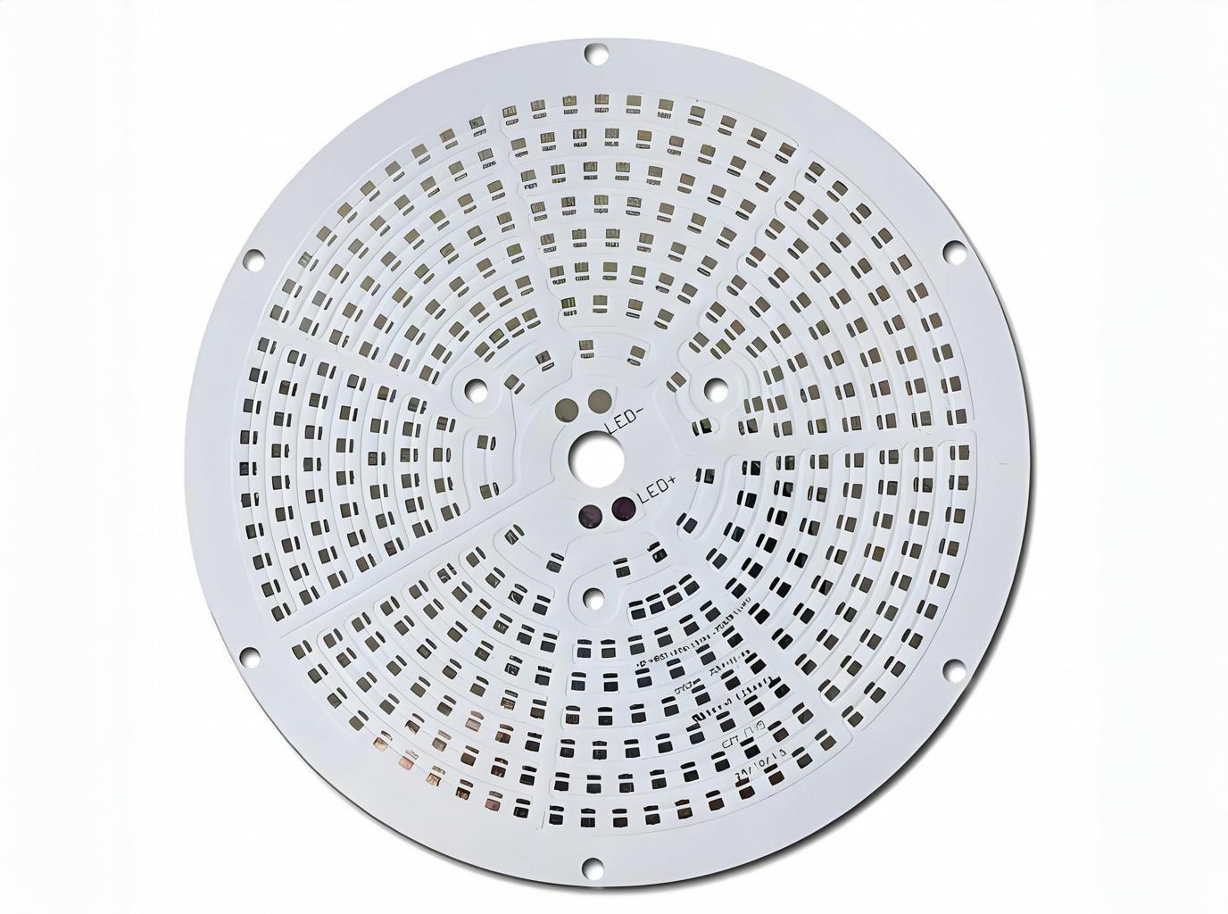
What Is the Meaning of MCPCB LED Plate?
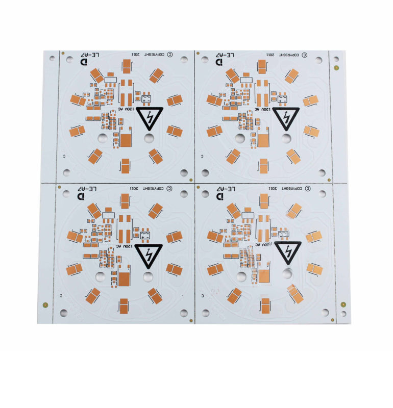
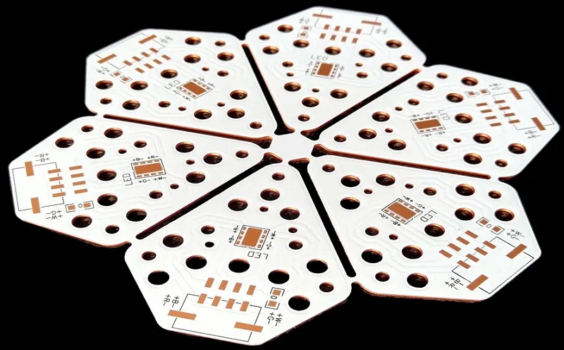
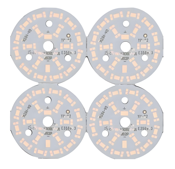
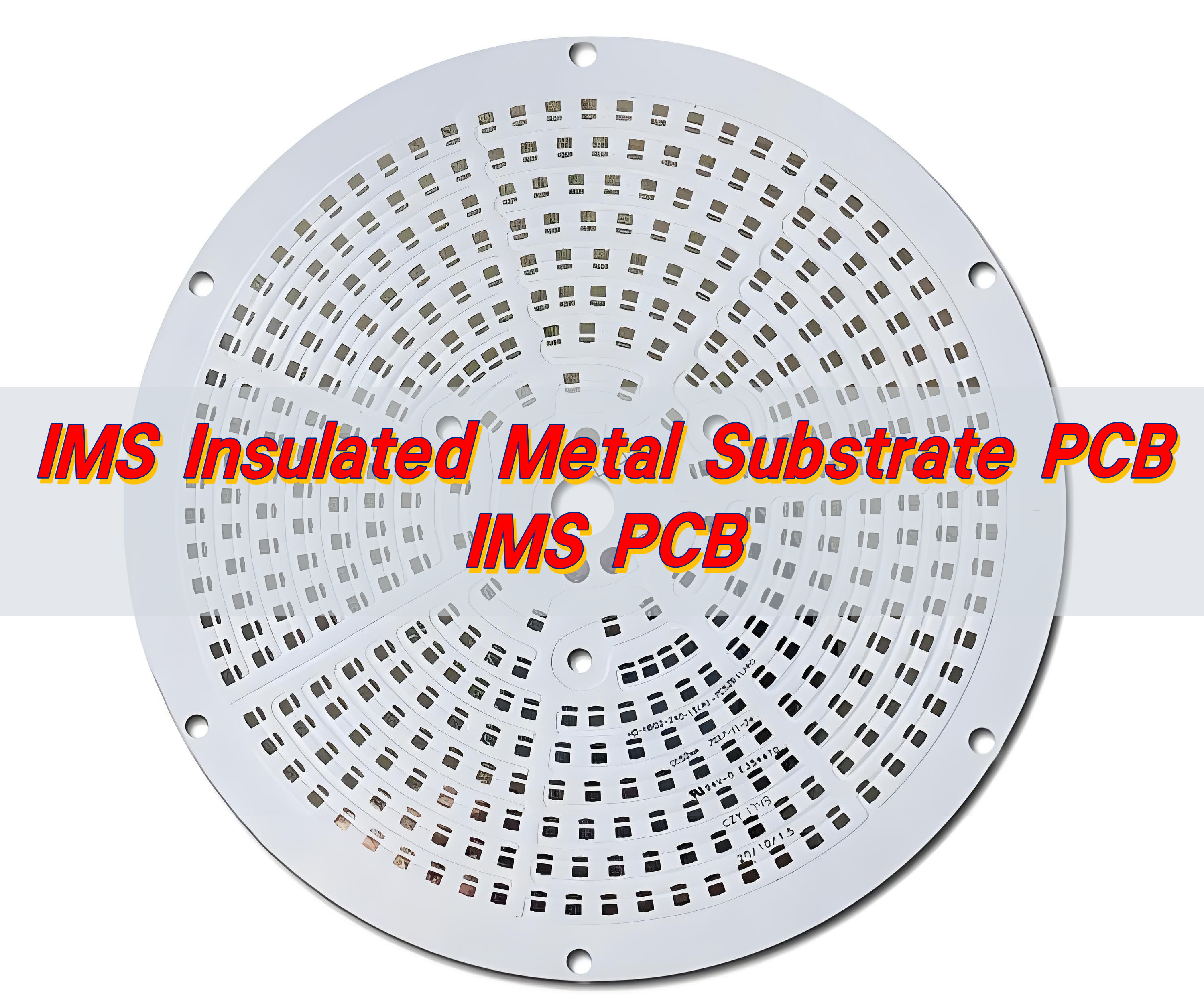
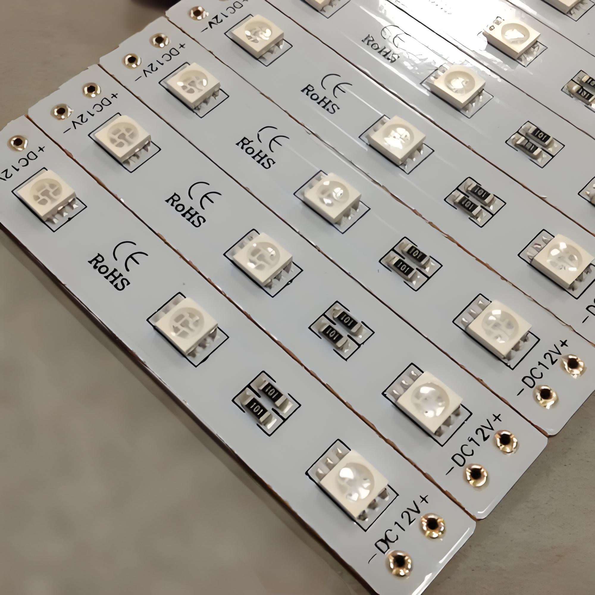
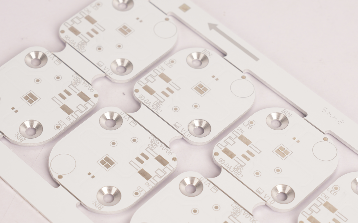
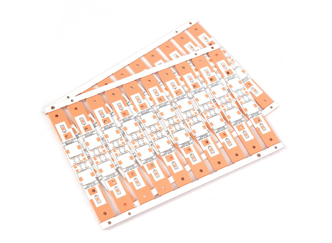
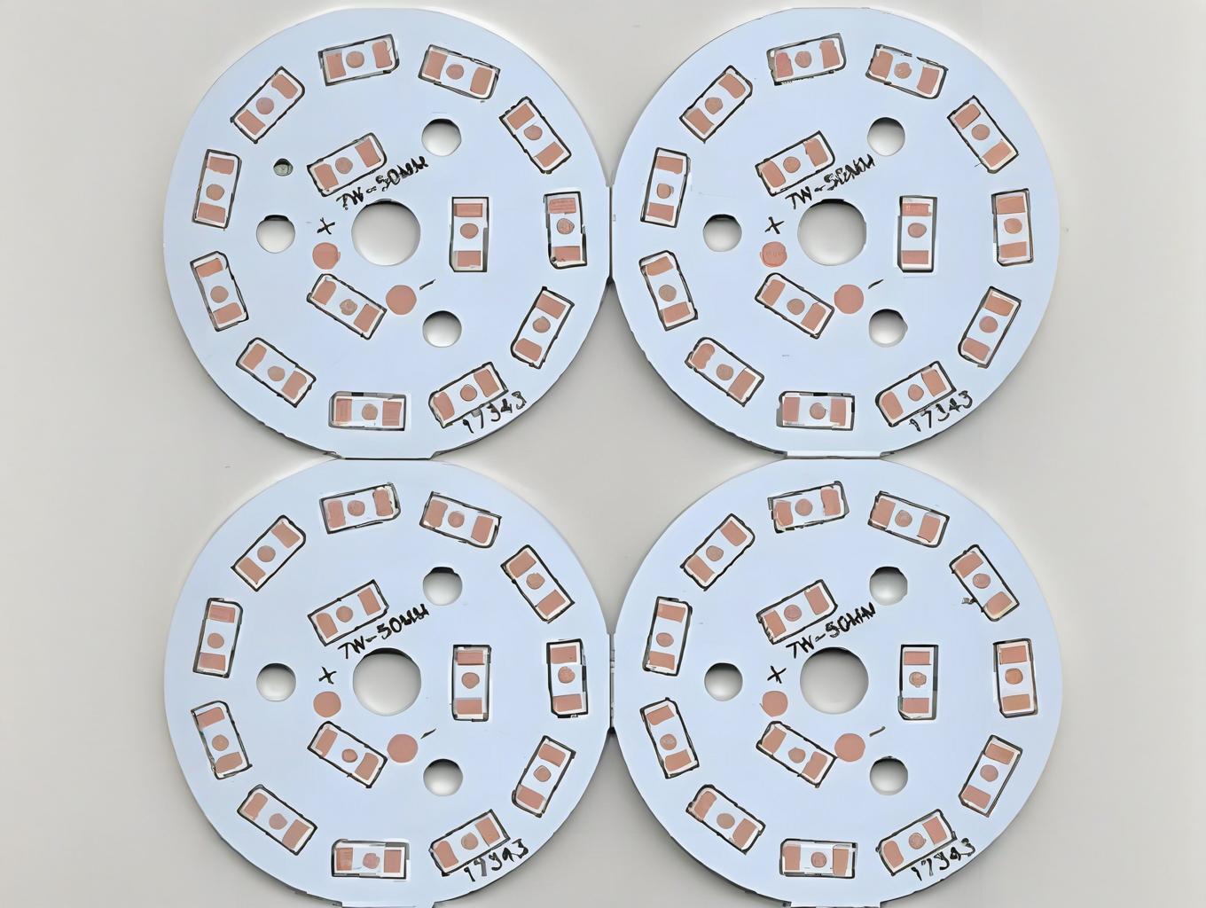
A MCPCB LED plate refers to a Metal Core Printed Circuit Board (MCPCB) specifically engineered for LED lighting applications. It features a metal base (typically aluminum or copper) as the core material, bonded with a thermally conductive dielectric layer and a copper circuit layer. Designed to efficiently dissipate heat generated by high-power LEDs, it ensures optimal performance, reliability, and longevity of LED modules, fixtures, or displays by preventing overheating. Commonly used in automotive lighting, streetlights, and high-brightness LED systems.
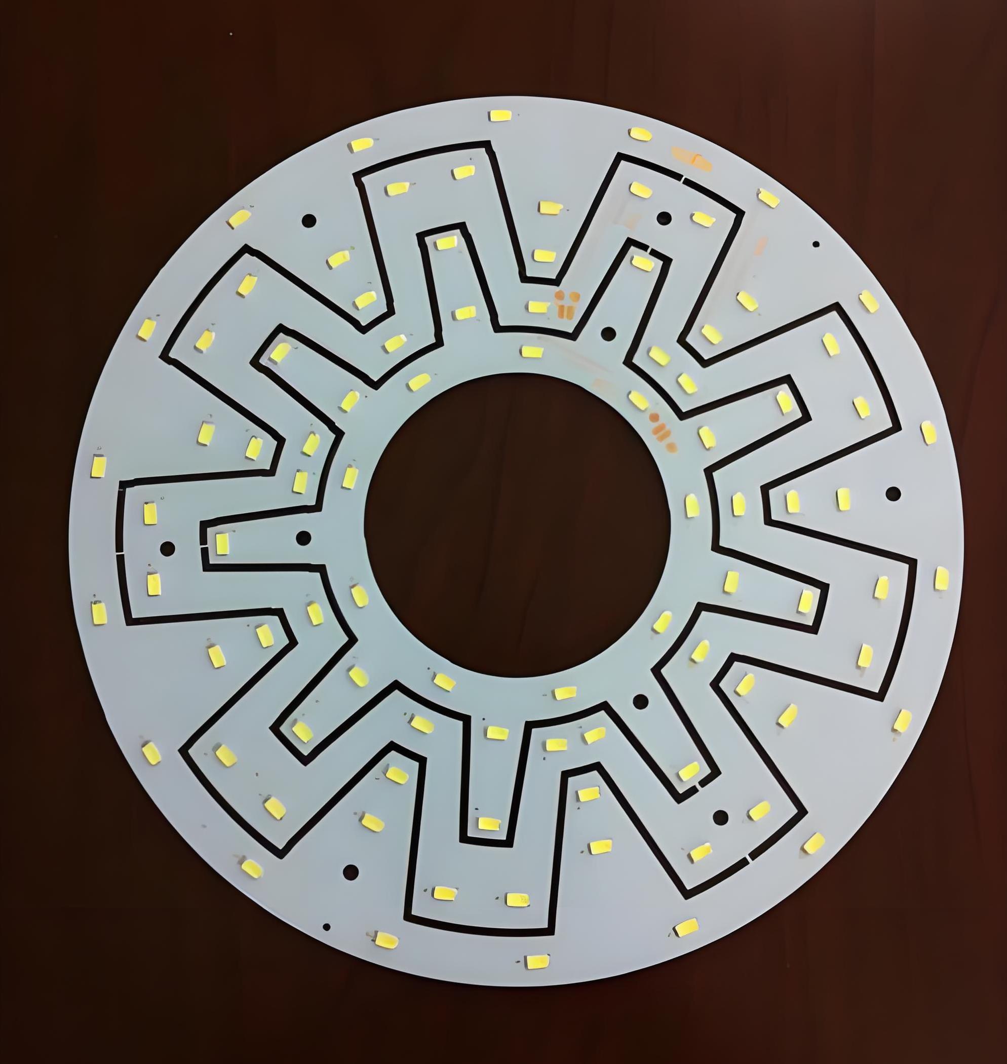
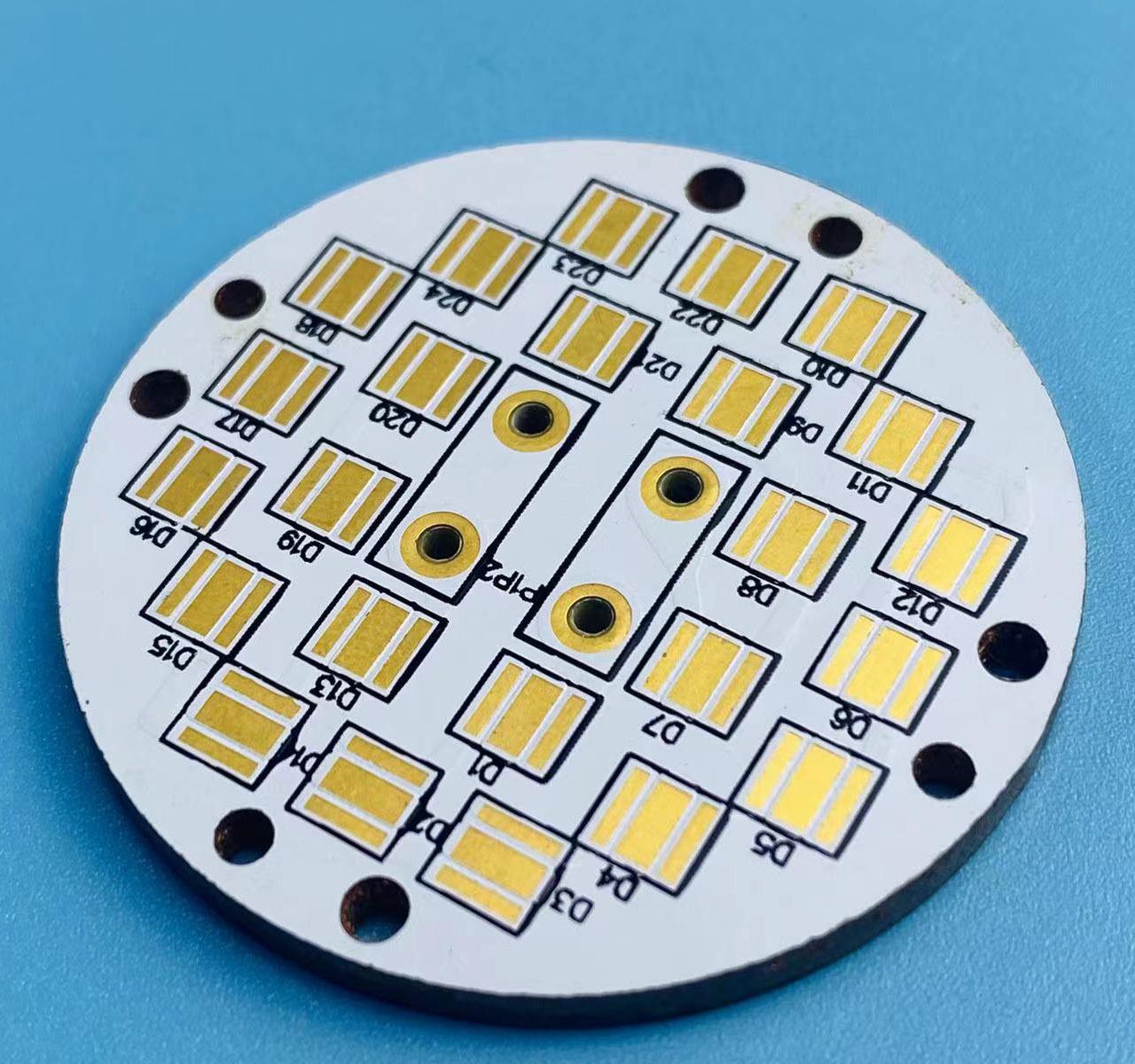
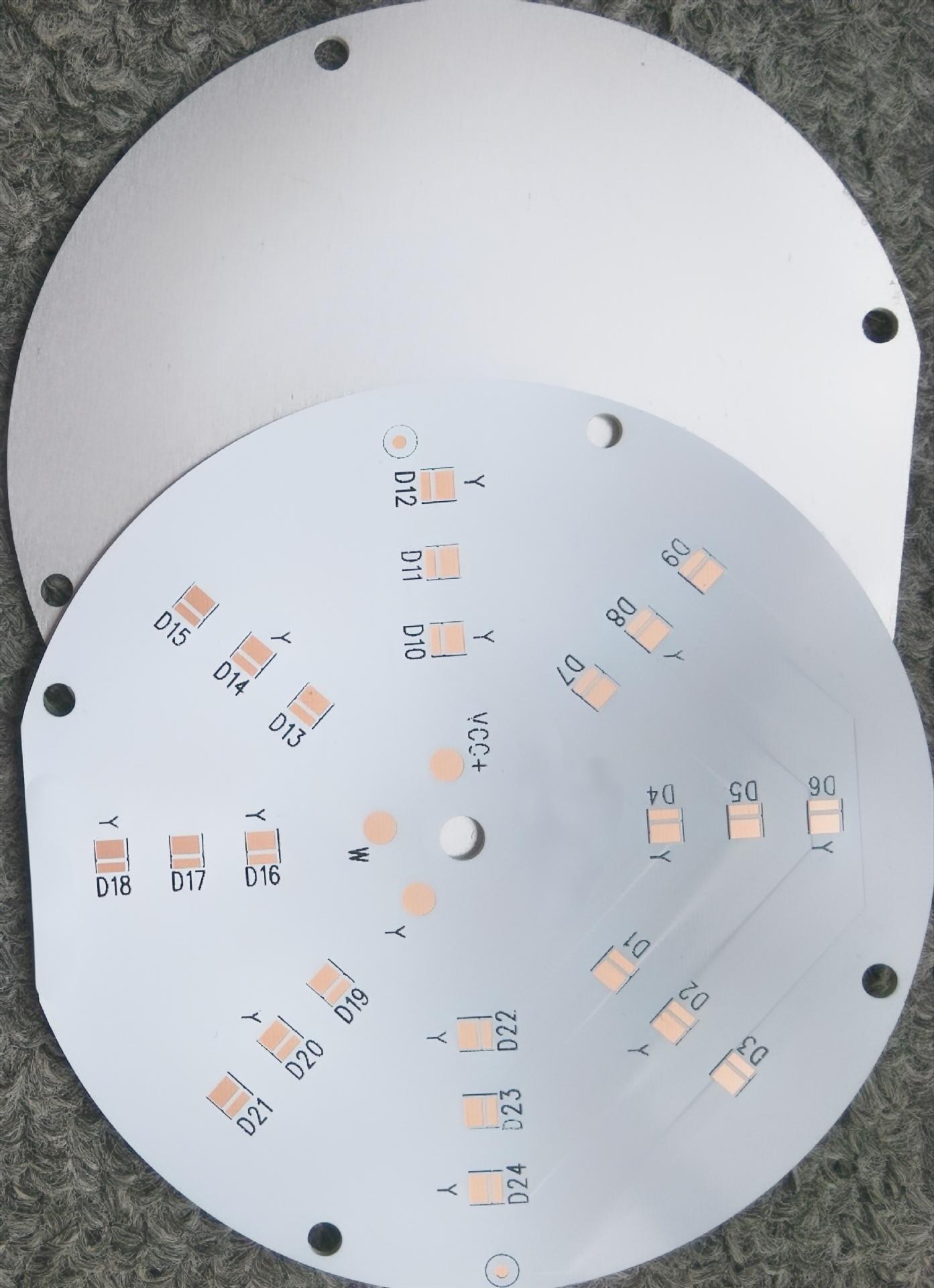
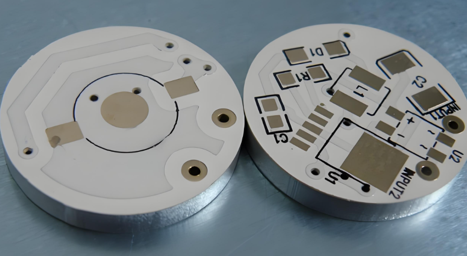
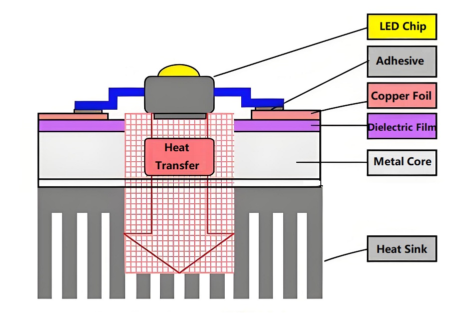
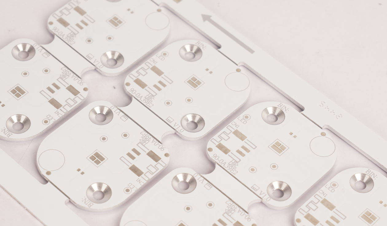
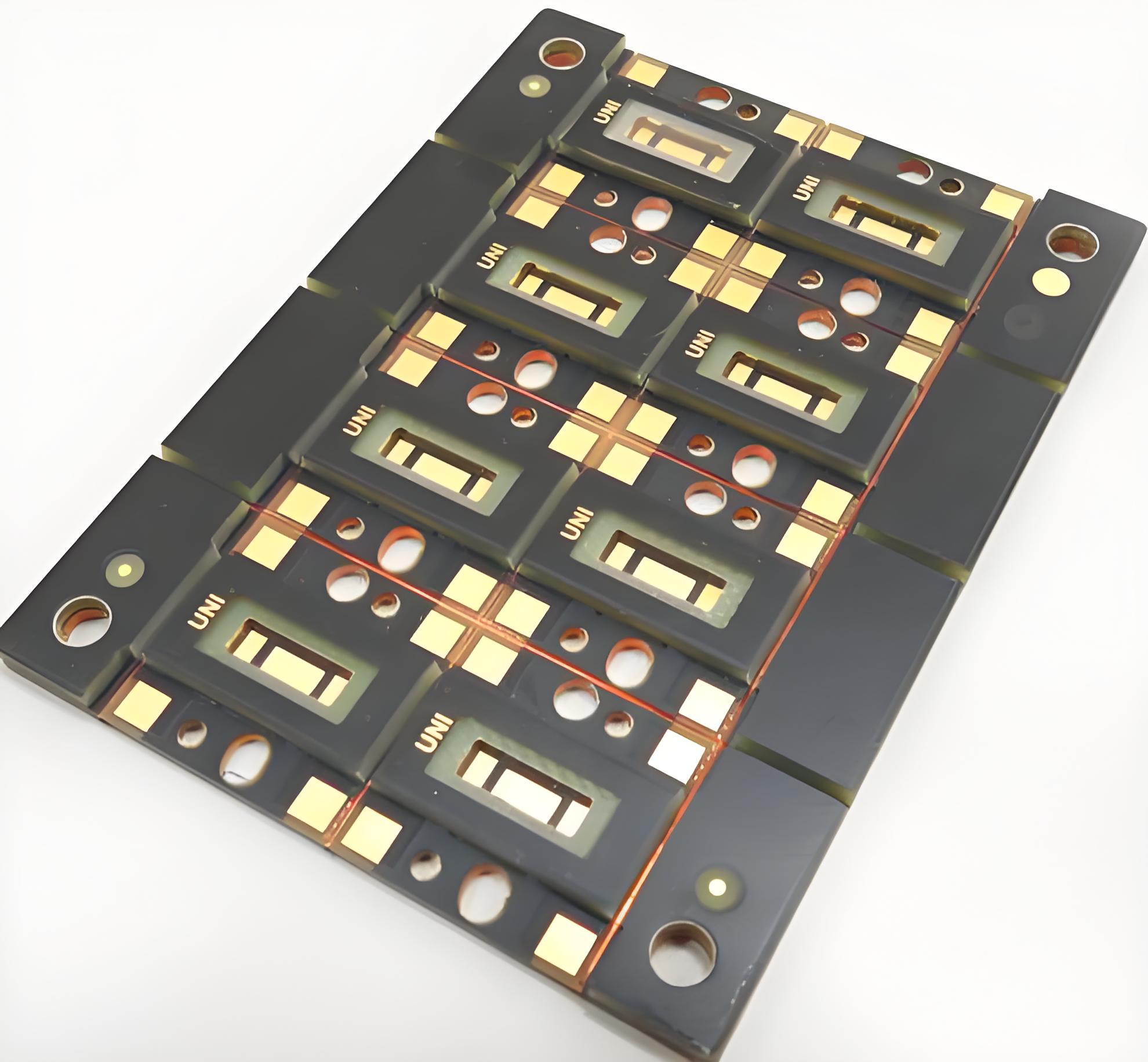
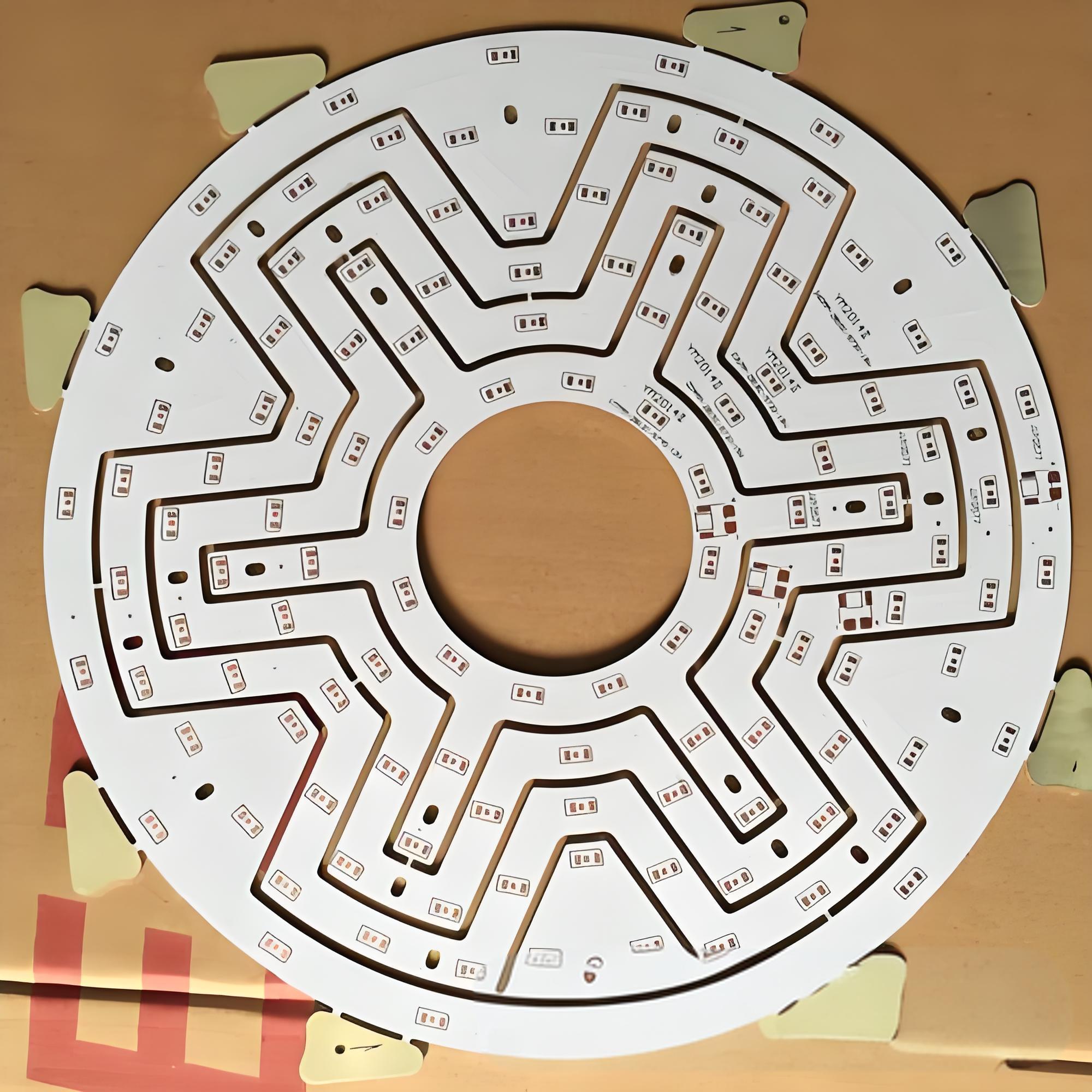
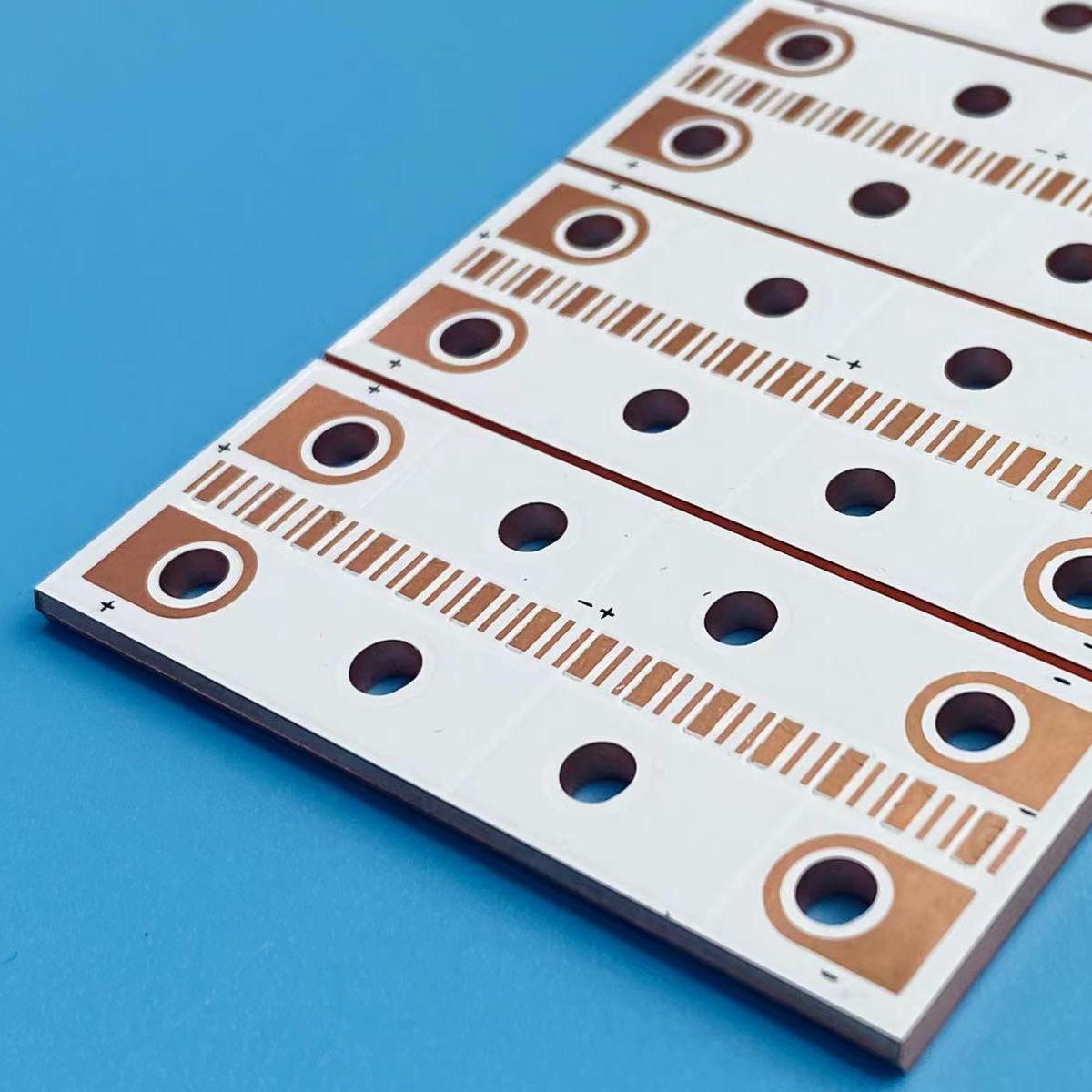
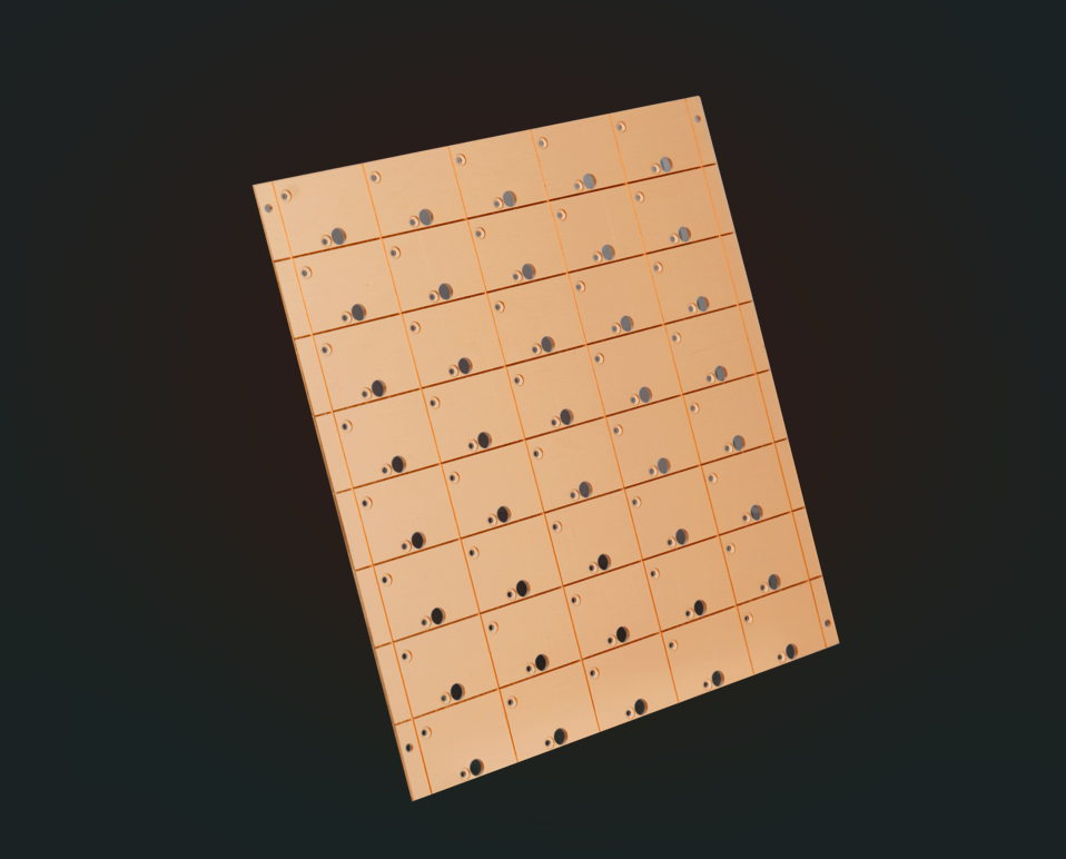
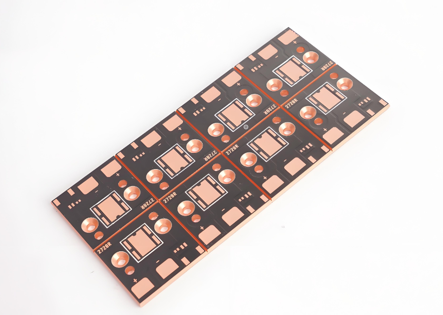
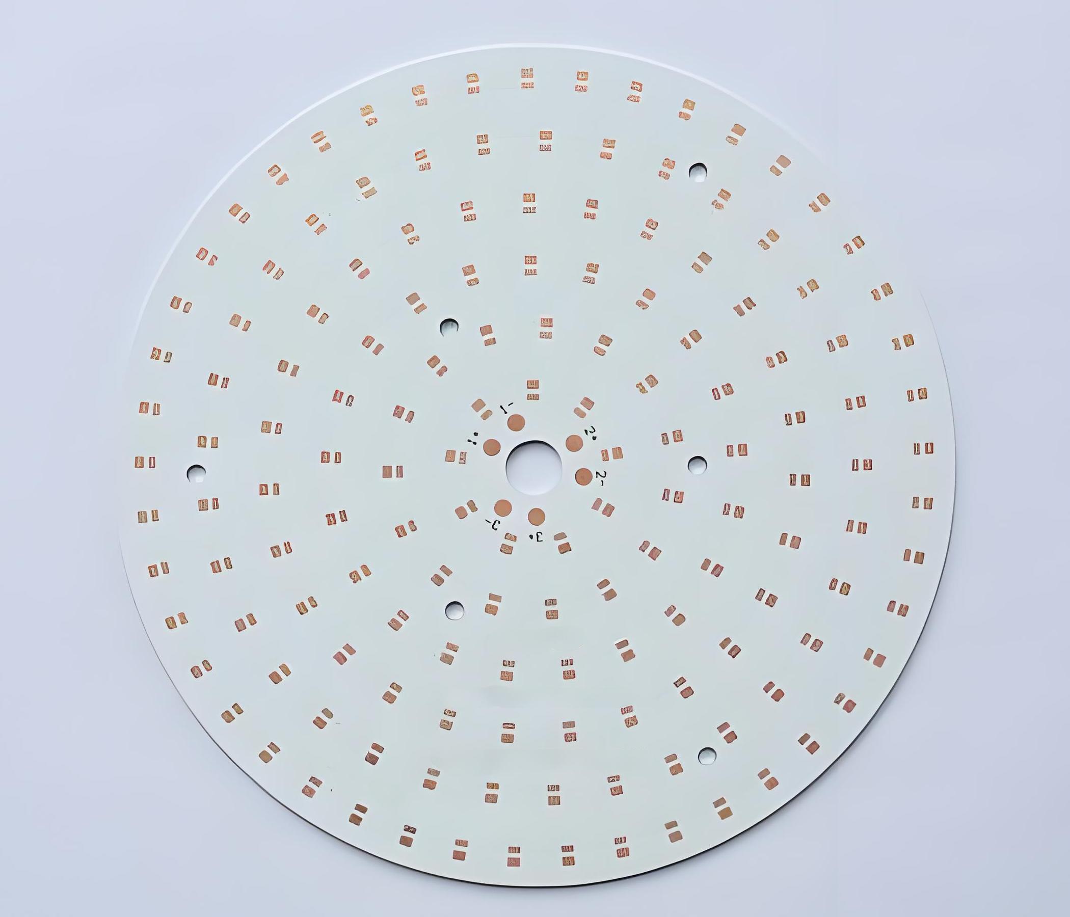
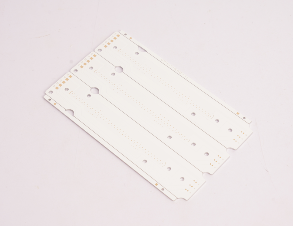
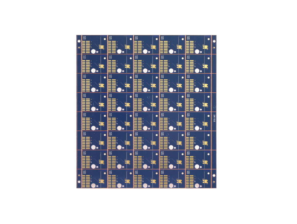
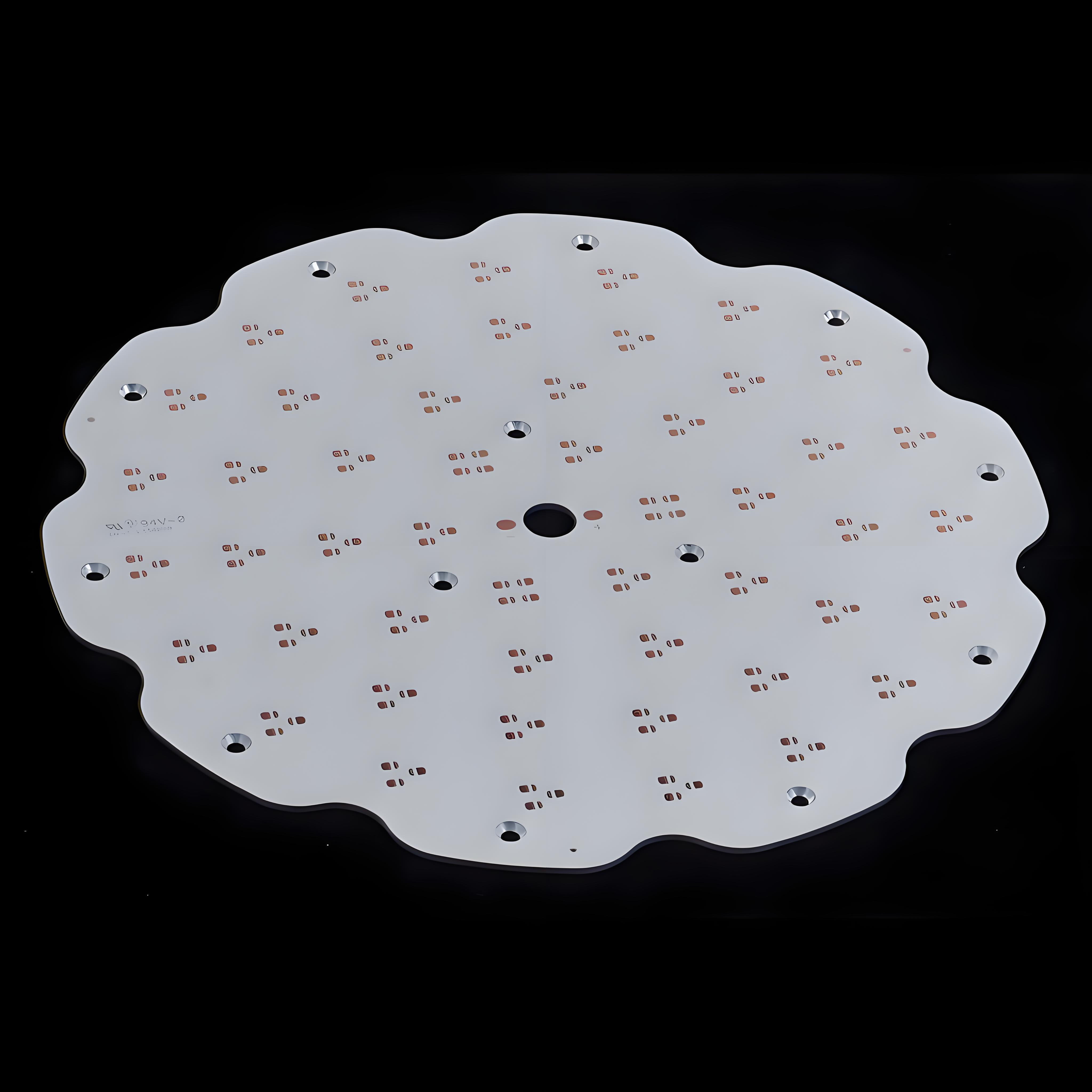
MCPCB LED PCB Construction
Metal Base Layer
- Material: Aluminum (most common) or copper.
- Function: Acts as a heat sink, drawing thermal energy away from LEDs to prevent overheating and extend component lifespan.
Dielectric Layer
- Material: Thermally conductive epoxy or ceramic-filled prepreg.
- Function: Electrically isolates the metal base from copper traces while enabling efficient heat transfer (thermal conductivity: 1–8 W/m·K).
Copper Circuit Layer
- Thickness: 1–10 oz (35–350 µm).
- Function: Transmits electrical signals and power to LEDs; thicker copper (≥2 oz) supports high-current applications (>3A per trace).
Solder Mask Layer
- Material: Epoxy-based or polyimide coating.
- Function: Protects copper traces from oxidation, solder bridging, and environmental contaminants (e.g., moisture, dust).
Surface Finish
- Options: HASL (cost-effective), ENIG (flat surface for fine-pitch SMT), or OSP (organic solderability preservative).
- Function: Ensures reliable solder joints during assembly and prevents corrosion.
How Does the MCPCB LED Plate Work?
- Heat Generation: LEDs convert electrical energy into light, generating waste heat (typically 50–70% of input power).
- Thermal Conduction: Heat transfers from LED junctions through solder joints to the copper circuit layer.
- Dielectric Layer Transfer: The thermally conductive dielectric (epoxy/ceramic) rapidly channels heat from copper traces to the metal base.
- Metal Base Dissipation: Aluminum/copper base acts as a heat sink, spreading heat across its surface area and radiating it into the environment.
- Cooling Efficiency: Reduces LED junction temperature by 20–40% compared to FR4 PCBs, preventing lumen degradation and color shift.
- Performance Impact: Maintains LED efficacy (>90% initial brightness) and lifespan (>50,000 hours) by avoiding thermal runaway.
What Are Application of MCPCB LED Board?
- Automotive Lighting – Headlights, brake lights, DRLs. Ensures reliability in high-temperature engine environments.
- Outdoor Street Lighting – Solar-powered streetlights, floodlights. Enables compact, weather-resistant designs with minimal maintenance.
- Industrial High-Bay Lighting – Warehouses, factories. Stabilizes performance in dusty/hot conditions, cutting energy costs.
- Horticultural Grow Lights – Vertical farming, indoor agriculture. Maintains spectral accuracy for faster plant growth.
- UV LED Systems – Curing, medical sterilization. Prevents wavelength shifts from overheating, ensuring precision.
- Consumer Electronics Backlighting – TVs, laptops, smartphones. Enables thin profiles while preserving brightness and battery life.
MCPCB LED Plate Design Guide
Below is MCPCB LED plate design guideline:
1. Metal Base Selection
- Aluminum (6061/5052): Lightweight, cost-effective, ideal for general LED lighting (streetlights, indoor fixtures).
- Copper: Higher thermal conductivity (3–4× aluminum) for ultra-high-power applications (automotive headlights, UV curing).
- Avoid: Steel (poor thermal performance) or overly thick metals (increases cost/weight without proportional gains).
2. Circuit Layer Design
- Copper Thickness: Use ≥2 oz (70 µm) for currents >3A/trace; ≥4 oz (140 µm) for >5A.
- Trace Width: Follow IPC-2221 standards (e.g., 10 mm width for 5A at 10°C rise).
- Via Design: Place thermal vias (0.3–0.5 mm diameter, 1:1 pitch) under LED pads to channel heat to the metal base.
3. Dielectric Layer Optimization
- Thermal Conductivity: Aim for ≥2 W/m·K (e.g., ceramic-filled epoxy). Avoid low-conductivity fillers (<1 W/m·K).
- Thickness: Keep ≤100 µm to balance insulation and heat transfer. Thicker layers reduce thermal efficiency.
4. Thermal Management Integration
- Heat Sink Attachment: Use thermal gap pads (1–5 W/m·K) or direct metal-to-metal bonding for passive cooling.
- Active Cooling: For >50W/cm² heat loads, add embedded heat pipes or miniature fans (requires PCB hole design).
5. Surface Finish
- ENIG (Electroless Nickel/Immersion Gold): Best for fine-pitch SMT assembly (e.g., 0.4 mm pitch LEDs).
- HASL (Hot Air Solder Leveling): Cost-effective for through-hole components; avoid for high-frequency signals.
6. Design Verification
- Thermal Simulation: Use ANSYS Icepak to model junction temperatures before prototyping.
- Testing: Validate under worst-case conditions (e.g., 85°C ambient, 100% load) to ensure ≤10°C delta between junction and case.
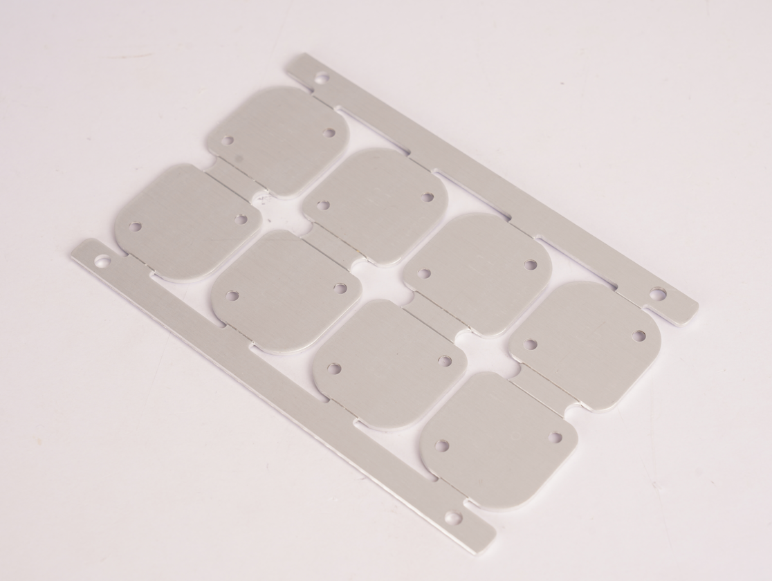
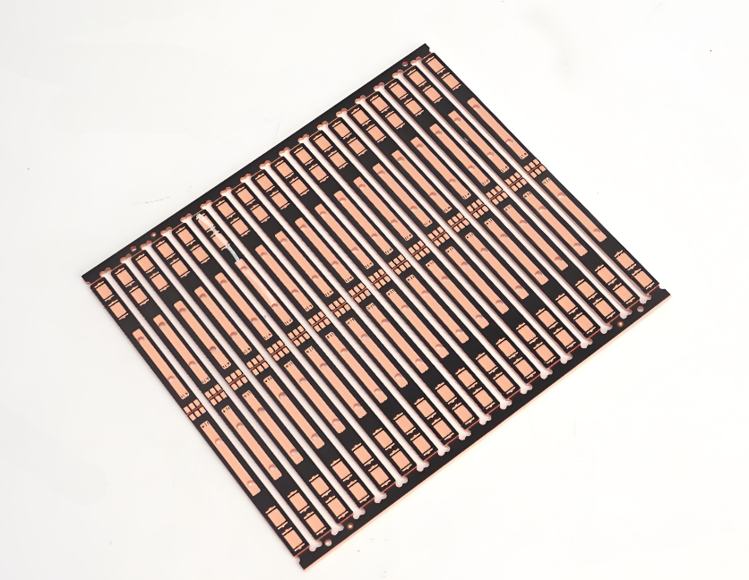
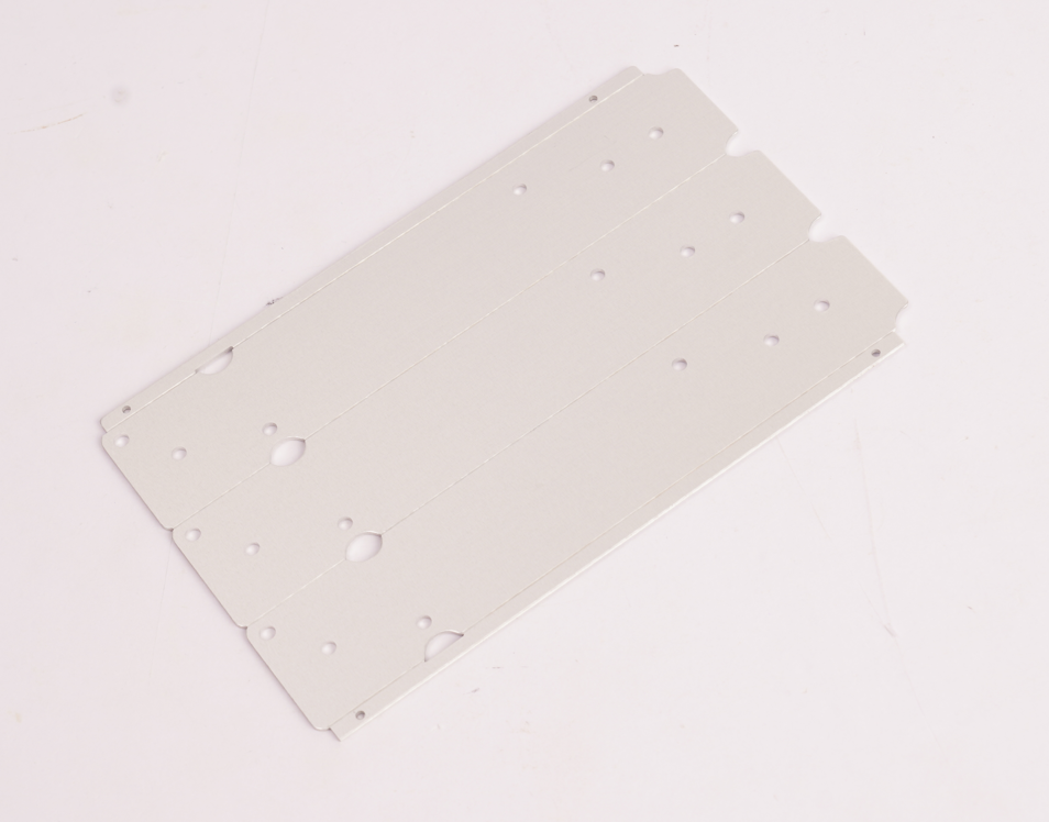
Metal Core PCB LED Plate Manufacturing Processes
MCPCB LED plate manufacturing processes:
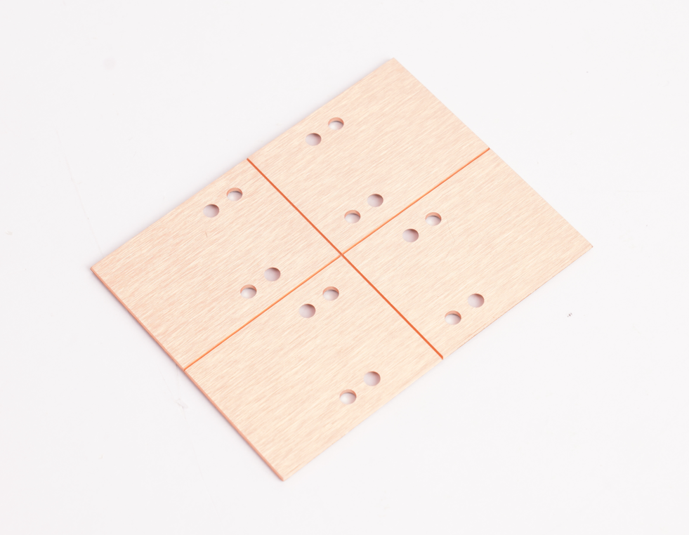
1. Material Cutting
- Metal Base: Cut aluminum (5052/6061) or copper sheets to panel size (e.g., 12″×18″).
- Copper Foil: Slice thin copper sheets (1–4 oz thickness) to match metal base dimensions.
2. Surface Pretreatment
- Metal Base: Ultrasonic clean + chemical etch (e.g., NaOH) to remove oils/oxides, improving adhesion.
- Copper Foil: Micro-etch (H2SO4 + H2O2) to roughen surfaces for better dielectric bonding.
3. Dielectric Layer Application
- Coating: Roll-coat ceramic/epoxy-based thermal interface material (TIM) onto the metal base (thickness ≤100 µm).
- Curing: UV or thermal curing (150–180°C, 30–60 mins) to solidify the layer.
4. Copper Foil Lamination
- Stacking: Align pre-treated copper foil over the cured dielectric layer.
- Pressing: Hot-press (180–200°C, 40–60 kg/cm²) to bond copper foil to the dielectric, forming a single-layer structure.
5. Circuit Formation
- Dry Film Lamination: Attach photosensitive film to copper foil.
- Exposure & Development: UV image transfer to define traces; alkaline wash removes unexposed film.
- Etching: Chemical removal (CuCl2 + HCl) of unprotected copper, leaving precise circuitry.
6. Drilling
- Mechanical Drilling: CNC drill via holes (diameter ≥0.2 mm) for LED mounting and thermal vias.
- Deburring: Remove drilling residues to ensure clean hole walls.
7. Surface Finish
- Electroless Nickel/Immersion Gold (ENIG): Apply 3–5 µm Ni + 0.05–0.1 µm Au for fine-pitch SMT soldering.
- HASL (Hot Air Solder Leveling): Tin coating for through-hole components (cost-effective alternative).
8. Testing & Inspection
- Electrical Test: Flying probe/AOI to detect shorts/opens.
- Thermal Validation: Simulate 85°C operation to verify heat dissipation (junction temp ≤120°C).
9. Cutting & Final QA
- Routing: CNC milling to separate panels into individual boards.
- Visual Inspection: 100% check for defects (e.g., scratches, incomplete plating).
10. Packaging & Shipping
- Vacuum Packaging: Moisture-resistant bags + desiccant to prevent oxidation.
- Labeling: Include lot number, RoHS compliance, and thermal performance specs.
How to Choose a Reliable MCPCB Manufacturer?
Methods about how to choose a trusted MCPCB LED plate Manufacturer:
Verify Certifications:
- Confirm ISO 9001/IATF 16949 (quality), UL (safety), and RoHS compliance.
- Cross-check certificates via official databases (e.g., UL’s online portal).
Inspect Material Quality:
- Request datasheets for thermal conductivity (e.g., aluminum: 1.0–4.0 W/m·K) and dielectric layer specs (thermal resistance <0.1°C·cm²/W).
- Ask for third-party lab reports or in-house test results (e.g., ion contamination checks).
Assess Production Equipment:
- Ensure factories use automated lines, CNC machines, and environmental testing chambers (e.g., thermal shock chambers).
- Check for advanced capabilities like laser drilling (microvias <0.1mm) or thermoelectric separation.
Evaluate Customization Flexibility:
- Confirm support for 1–8 layers, hybrid designs (FR4 + MCPCB), and surface finishes (ENIG, HASL, OSP).
- Inquire about rapid prototyping (e.g., 24-hour turnaround for single-layer boards).
Check Lead Time & MOQ:
- Confirm delivery timelines: 4–21 days for prototypes, 10–15 days for bulk orders (>1,000 pcs).
- Prioritize low MOQ (5–10 pcs) to minimize inventory risk.
Review Reputation:
- Prioritize suppliers with >10 years of MCPCB experience (e.g., E-CER: 30 years).
- Request client references (e.g., automotive or LED OEMs) and check online reviews.
Confirm Technical Support:
- Ensure engineers review Gerber files and provide DFM (Design for Manufacturability) feedback.
- Verify failure analysis capabilities (e.g., X-ray inspection, cross-sectioning).
- Clarify warranty terms (e.g., 1–2 years for material defects).
Compare Pricing Transparency:
- Request itemized quotes (material, labor, tooling) and avoid hidden fees (e.g., NRE costs).
- Negotiate volume discounts (10–30% off for orders >500 pcs).
How Much Does A MCPCB LED Board Cost?
MCPCB LED Board Price Range
- Standard Aluminum PCB (Single-layer, 1oz Cu): Around $0.05–$0.15/cm² (basic LED lighting).
- High-Thermal Copper PCB (Multi-layer, 2oz+ Cu): Around $0.30–$0.80/cm² (automotive/high-power applications).
- Prototype Costs (Small Batch): Around $50–$200/board (engineering fees included).
MCPCB LED Board Cost Influencers
- Substrate Material: Copper-based boards cost 2–3x aluminum due to superior thermal conductivity
- Layer Count: Multi-layer designs increase costs by 30–50% vs. single-layer
- Copper Thickness: 3oz heavy copper adds ~$0.08/cm²
- Surface Finish: Gold plating (ENIG) costs 20–40% more than HASL
- Order Volume: Bulk orders (>1,000pcs) reduce unit costs by 30–50%
For precise pricing, contact EBest Circuit (Best Technology) for a free DFM review and customized quote: sales@bestpcbs.com.