pcb
Home > Blog

Archive for the ‘Metal Core PCB’ Category

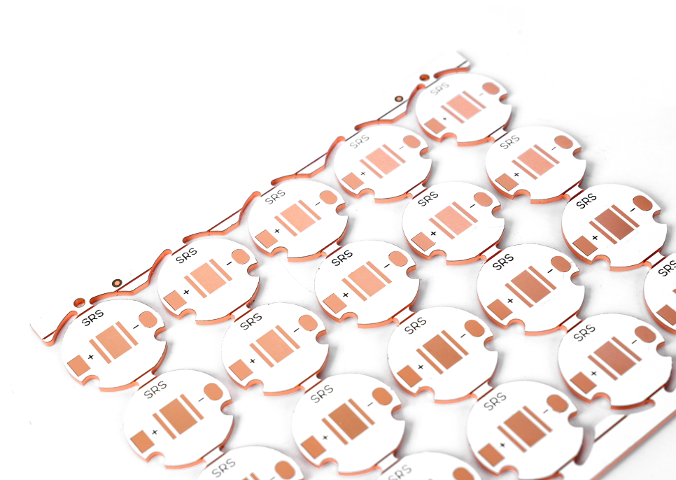
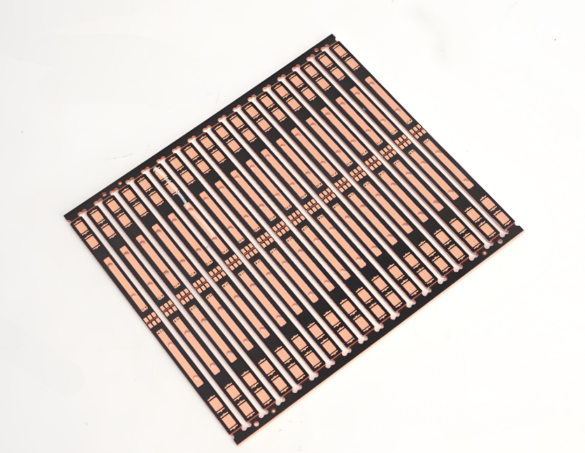
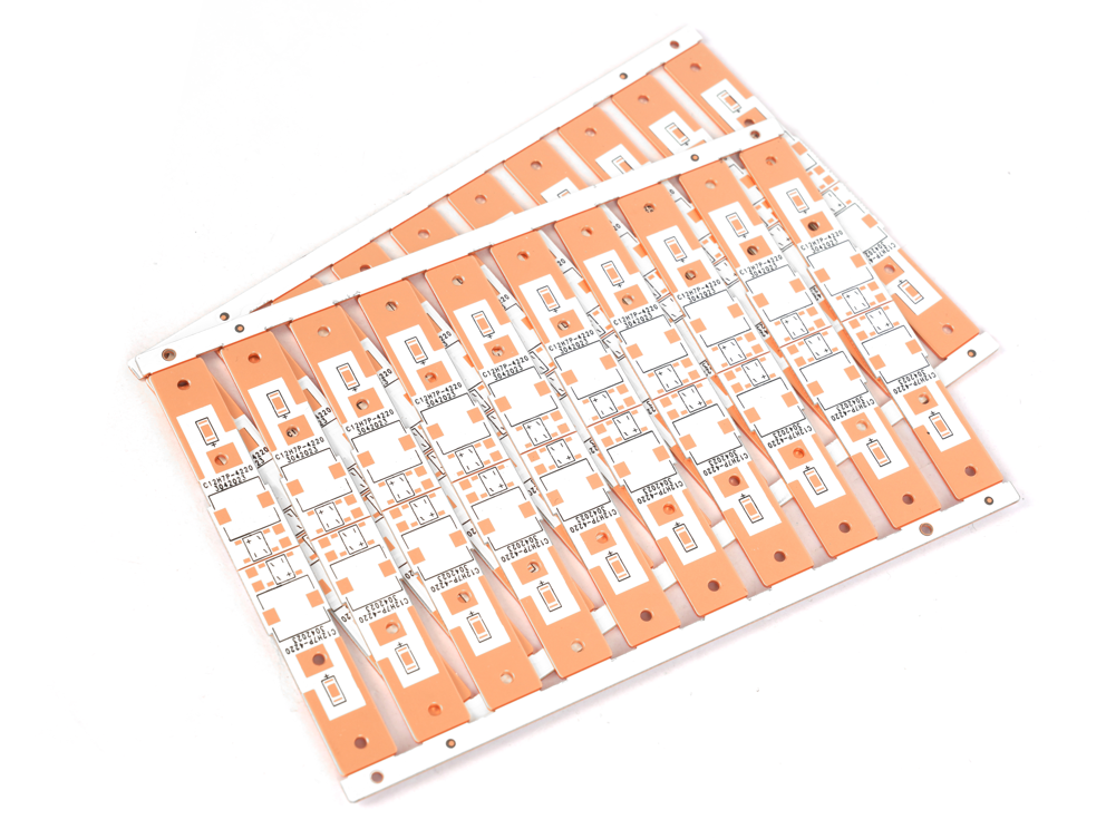
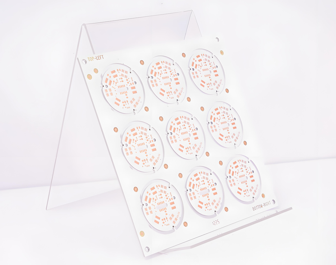
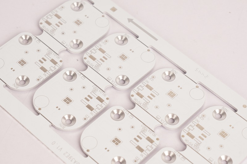
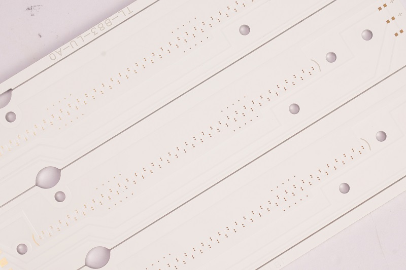
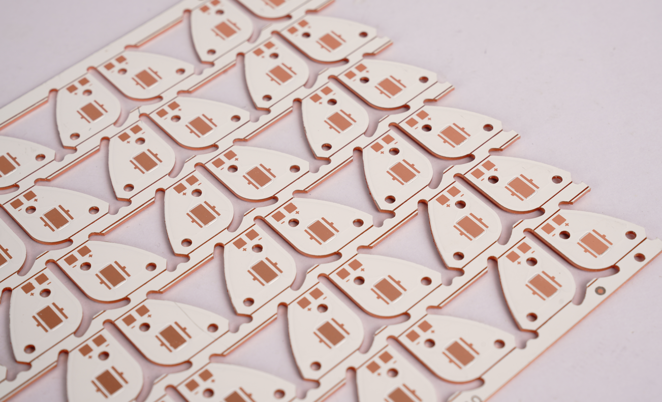
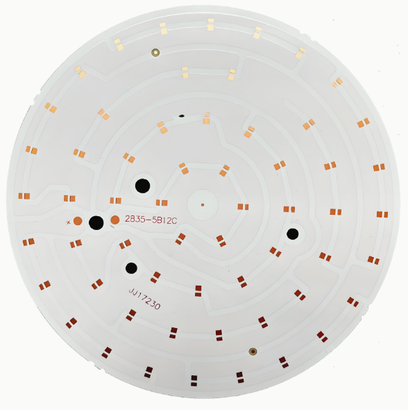
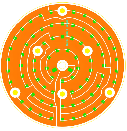
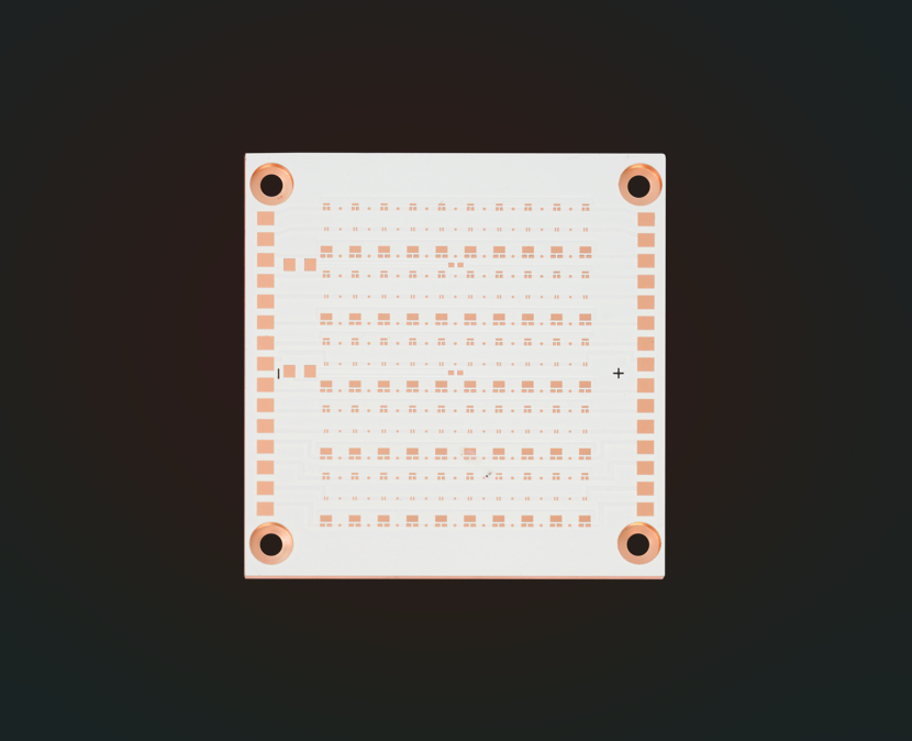
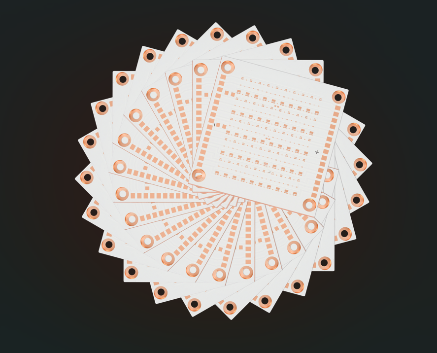
2L Aluminum Base PCB for LED Panel, Rapid Prototyping
Tuesday, July 1st, 2025

Looking for 2L aluminum base PCB prototyping solutions? This guide explores everything from material specs to cost-saving prototyping strategies for high-performance LED panel.

18 Years of Thermal Management Expertise – Your LED Panel’s Heat Dissipation Solved!

  • Thermal Throttling? – Our “Heat Tunnel” via design drops junction temps by 40%
  • Prototype Delays? – CAD-to-board in 24 hours with real-time DFM feedback
  • Signal Noise? – Isolated power planes maintain 65dB EMI suppression
  • Budget Constraints? – Standardized 300×400mm panels cut 12% tooling costs

Best Technology delivers:

  • Precision Thermal Control – 2L aluminum base PCB with 8W/m·K conductivity prevents LED lumen decay under 85°C continuous operation
  • Instant Prototyping – 24-hour rapid sampling with ±0.1mm drilling accuracy for design verification
  • Cost-Smart Design – Panelization-ready layouts reduce 15% material waste vs. standard FR4
  • Vibration Resistance – 1.5mm aluminum substrate withstands 20G mechanical shock in outdoor LED displays

Every 2L Aluminum base PCB – A Thermal Guardian for Brighter LED Performance! Welcome to contact us now: sales@bestpcbs.com.

What Is 2L Aluminum Base PCB?

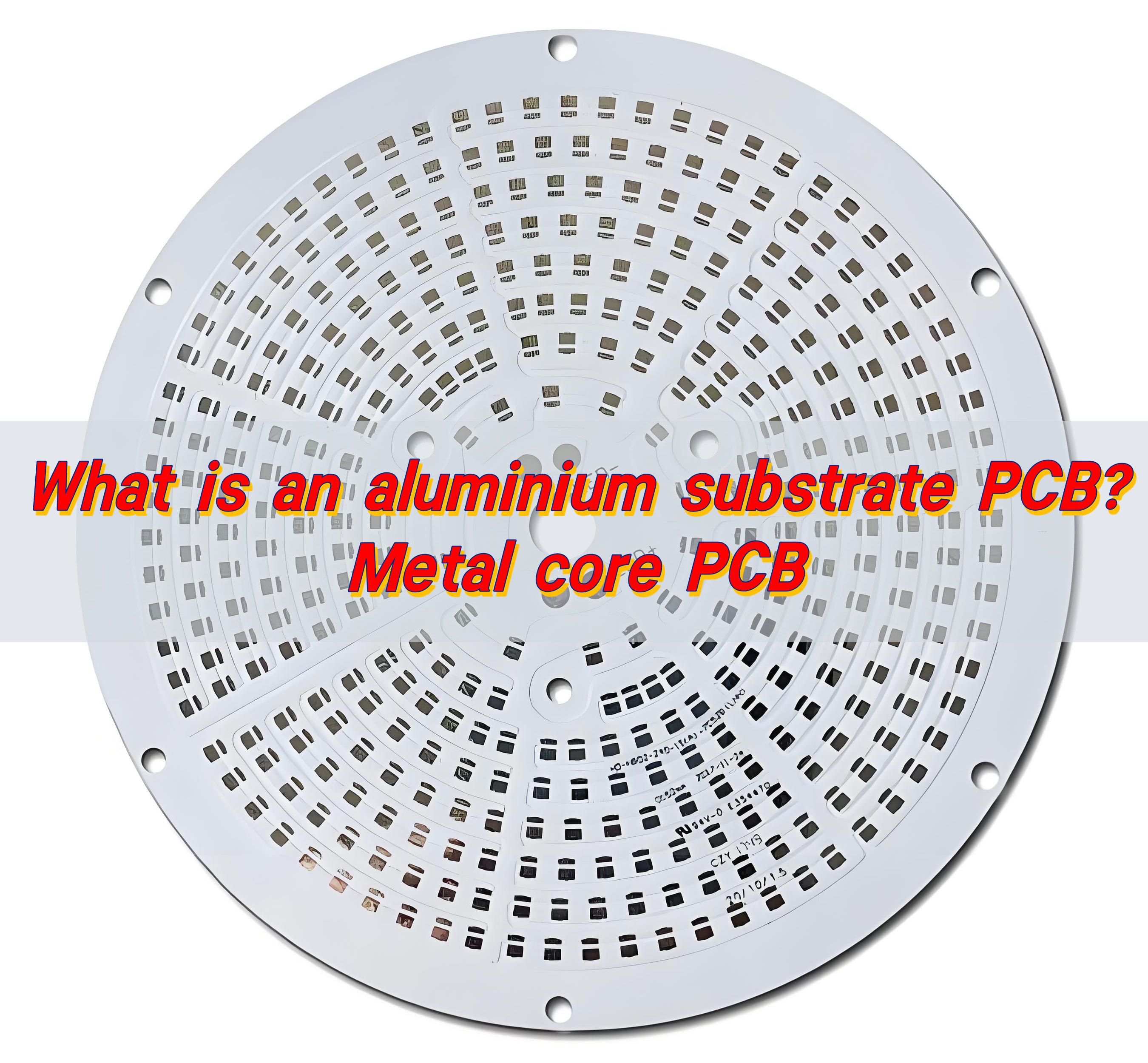
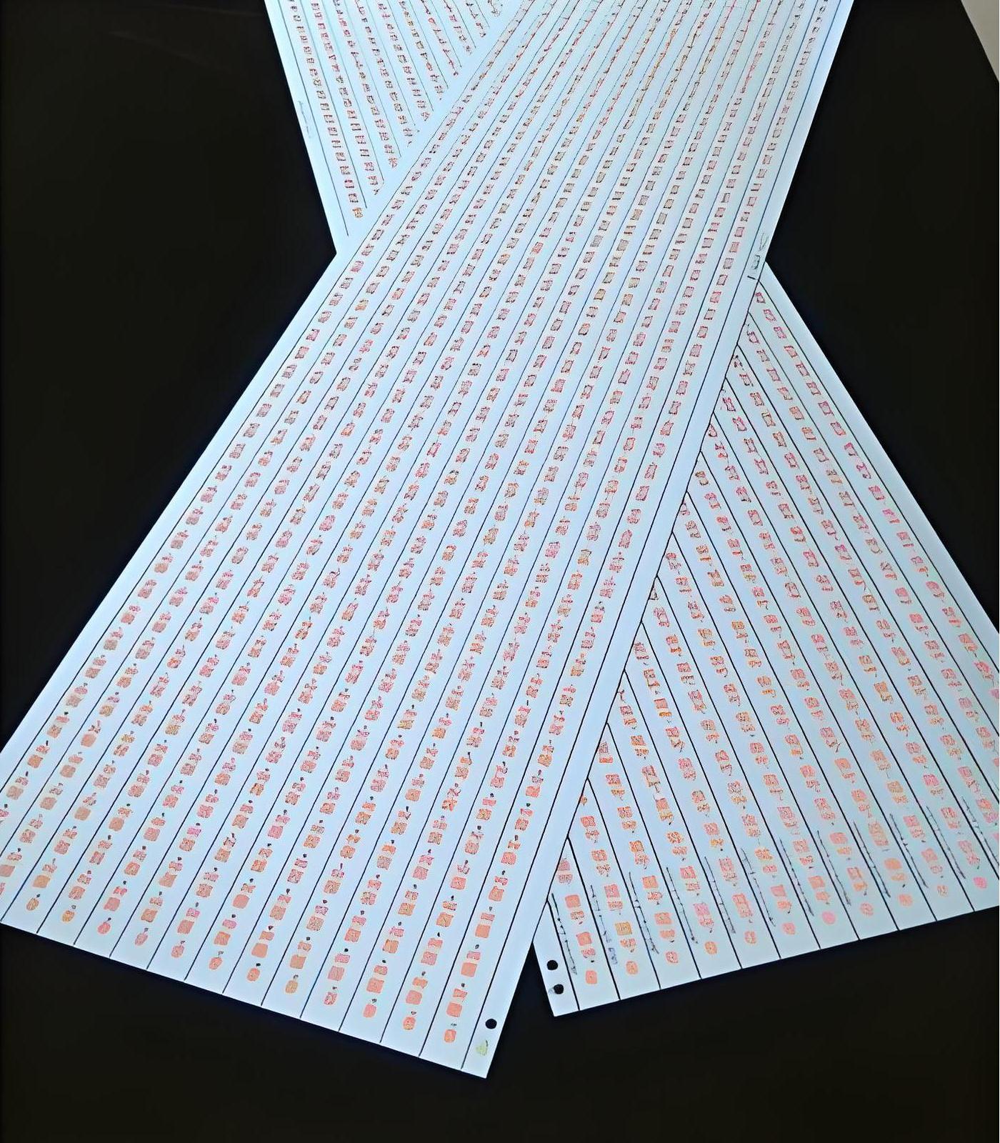
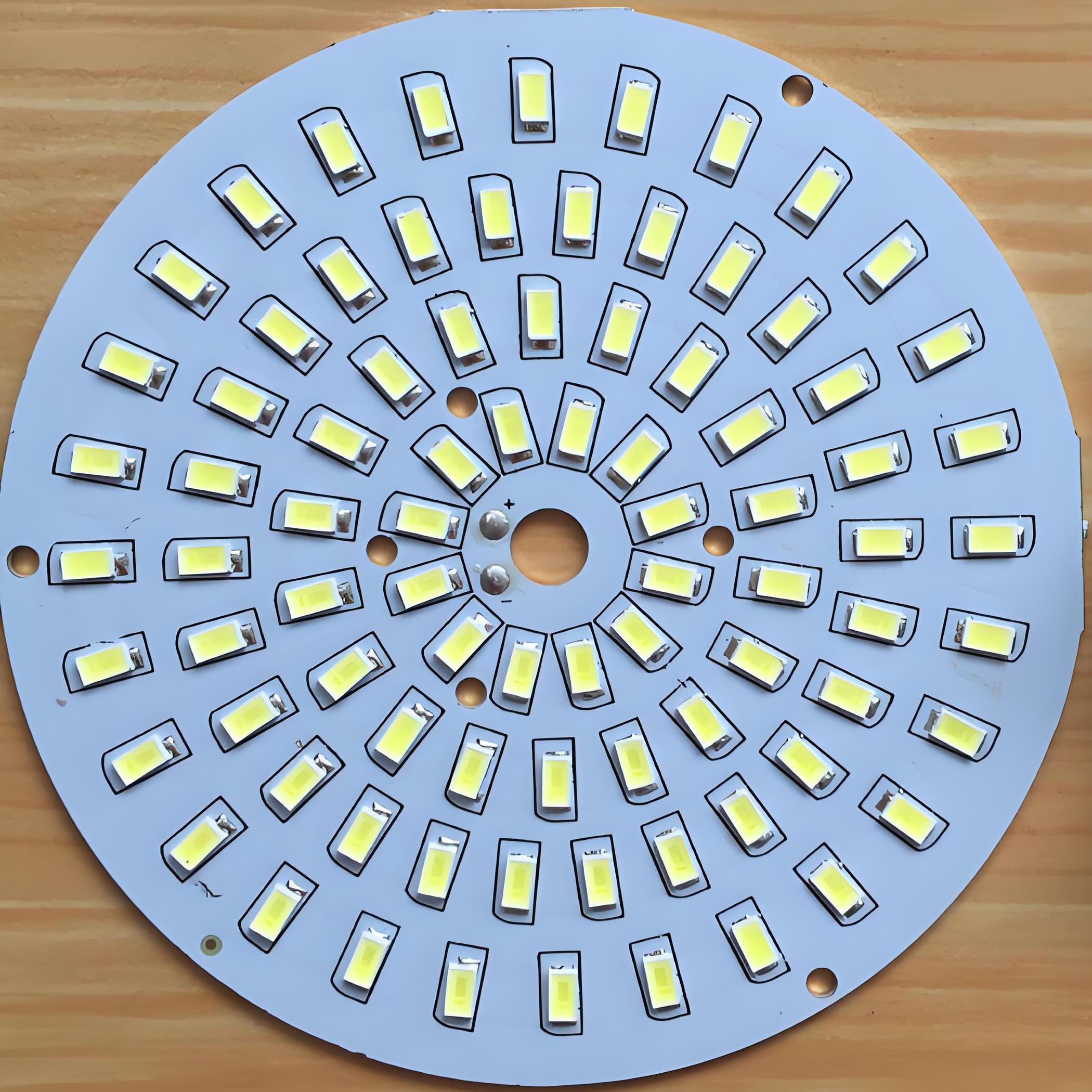
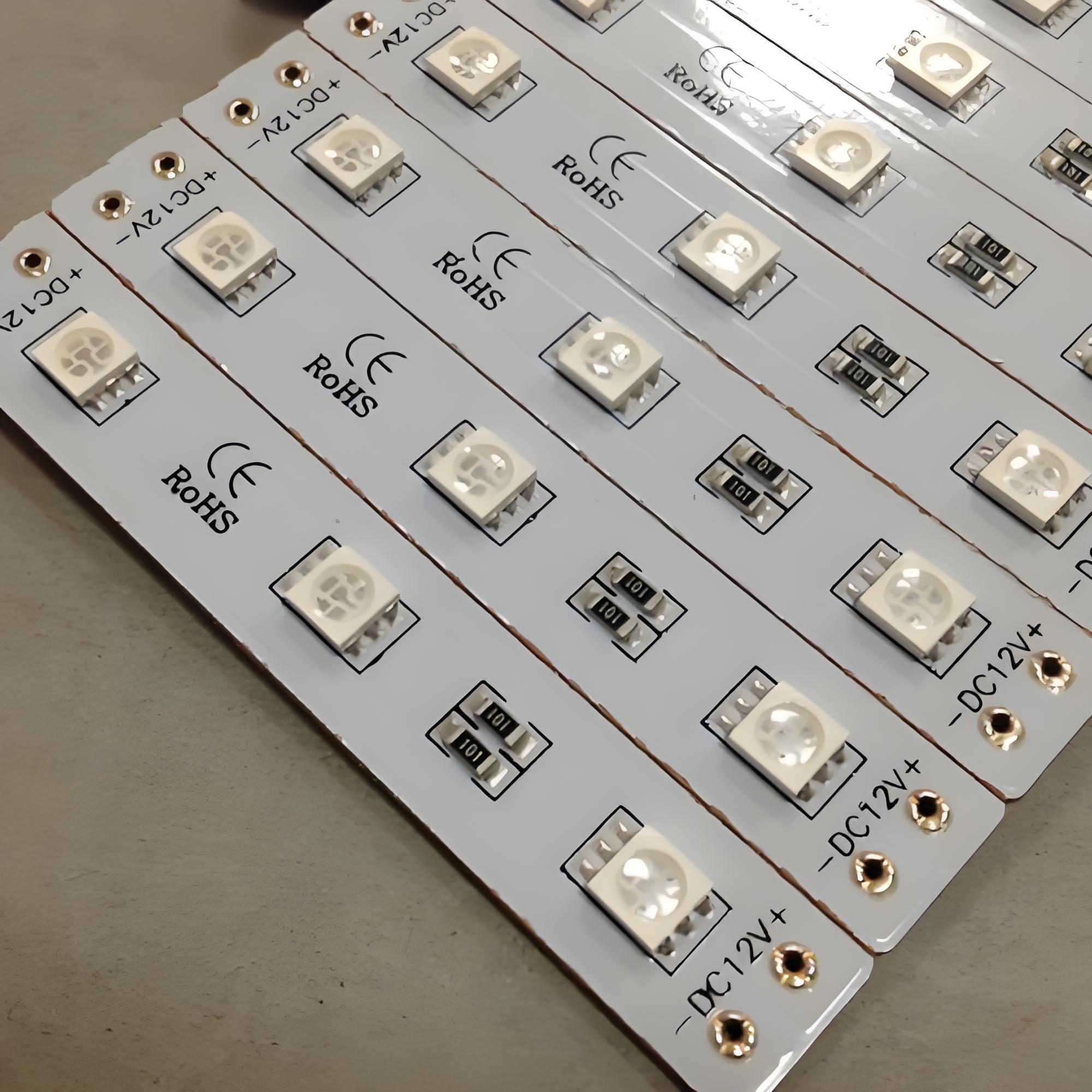
A 2L aluminum base PCB, also known as a double-layer aluminum substrate printed circuit board, is a specialized type of PCB designed for applications requiring efficient heat dissipation and mechanical stability. Unlike traditional PCBs, it features a layered structure with a conductive circuit layer bonded to an aluminum base, which acts as a heat sink to quickly transfer and disperse thermal energy.

This design makes 2L Aluminum Base PCBs particularly useful in high-power LED lighting, power converters, and automotive electronics, where managing excessive heat is essential for performance and longevity. The aluminum core not only enhances thermal conductivity but also provides structural rigidity, reducing warping under thermal stress. Additionally, the double-layer configuration allows for more complex circuitry while maintaining compact dimensions.

Due to their durability and thermal management capabilities, these PCBs are increasingly preferred in industries where reliability and heat resistance are priorities. Their construction typically includes a dielectric layer to ensure electrical insulation between the circuit and the metal base, balancing electrical functionality with thermal efficiency.

What Is 2L Aluminum Base PCB?

What Is Stackup Structure of 2L Aluminum Base PCB?

Below are the stackup structure of a 2L aluminum base PCB:

Top Copper Layer (Circuit Layer)‌

  • Typically 1–4 oz copper foil thickness
  • Contains etched conductive traces and component mounting pads
  • Supports surface-mount device (SMD) assembly

Dielectric Insulation Layer‌

  • Composed of thermally conductive polymer (e.g., polyimide or epoxy) with ceramic fillers
  • Thickness ranges 0.003–0.006 inches (75–150 ÎŒm)
  • Provides electrical isolation while enabling heat transfer

Aluminum Base Plate‌

  • 0.5–3.0 mm thick aluminum alloy (usually 5052 or 6061 grade)
  • Functions as primary heat spreader and mechanical support
  • May include anodized surface treatment for corrosion resistance

Bottom Copper Layer (Optional Secondary Circuit Layer)‌

  • Mirrors top layer capabilities when utilized
  • Enables double-sided component placement or grounding planes

Protective Surface Finishes‌

  • Top/bottom layers often feature HASL, ENIG, or OSP coatings
  • Aluminum base may have insulating conformal coating

Why Choose 2L Aluminum Base PCB for LED Panel?

Here are reasons to choose 2L aluminum base PCBs for LED panel applications:

  • Superior Heat Dissipation‌ – The aluminum core efficiently transfers heat away from LED chips, preventing overheating and extending lifespan by maintaining stable operating temperatures.
  • Enhanced Durability‌ – Aluminum’s structural rigidity reduces warping under thermal cycling, ensuring long-term reliability in high-power or continuous-use LED installations.
  • Improved Energy Efficiency‌ – Effective thermal management minimizes energy loss due to heat buildup, optimizing LED brightness and power consumption.
  • Compact Design Flexibility‌ – The double-layer construction allows complex circuitry in a slim profile, enabling sleek, space-saving LED panel designs without compromising functionality.
  • High Current Capacity‌ – Thicker copper layers (up to 10 oz) support robust electrical pathways, ideal for high-intensity LEDs or densely packed arrays.
  • Simplified Thermal Interface‌ – Eliminates the need for additional heat sinks in many designs, reducing assembly steps and material costs.
  • Consistent Light Output‌ – Stable temperature control prevents luminance degradation over time, maintaining uniform brightness across the LED panel.
Why Choose 2L Aluminum Base PCB for LED Panel?

How to Choose the Right 2L Aluminum PCB Prototype Manufacturer for Your LED Panel?

Methods about how to choose the right 2L aluminum PCB prototype manufacturer for your LED panel:

Verify Thermal Management Specialization

  • Confirm the manufacturer’s expertise in thermal simulation (e.g., ANSYS Icepak) for validating heat dissipation paths in your design. Request case studies demonstrating successful thermal solutions for LED arrays exceeding 100W. Ensure dielectric materials meet ≄1.5 W/mK thermal conductivity with UL 94 V-0 flame ratings.

Assess Aluminum-Specific Process Controls

  • Require documentation of aluminum substrate pretreatment (chemical cleaning, anodization) to prevent delamination. Validate micro-etching techniques maintaining ≀3ÎŒm copper line precision and AOI systems detecting 15ÎŒm defects. Thermal shock testing protocols (-40°C to +150°C cycling) should be mandatory.

Evaluate Rapid Prototyping Capabilities

  • Prioritize suppliers offering ≀72-hour prototype turnaround with live production tracking. Confirm readiness for engineering changes during fabrication without cost penalties. Small-batch capabilities (5-10 boards) with panelization efficiency ≄90% reduce material waste.

Scrutinize LED-Specific DFM Support

  • Demand manufacturers provide design rule checks (DRC) for high-current traces (≄3A/mmÂČ) and thermal pad optimization. Verify impedance control for mixed-signal designs and anti-caustic solder mask formulations resisting LED chemical exposure.

Confirm Multi-Stage Testing Protocols

  • Ensure 100% electrical testing includes HV isolation (≄1500V AC/DC) between layers and aluminum base. Require thermal imaging reports showing ≀15°C hotspot differentials across LED clusters. Microsection analysis should validate dielectric thickness consistency (±10%).

Review Scalability Pathways

  • Audit transition plans from prototypes to mid-volume production (1k-5k/month). Assess material inventory buffers for aluminum substrates and compatibility with automated SMT lines handling panel sizes ≄350×450mm.

Validate Supply Chain Transparency

  • Require full material traceability including aluminum alloy grades (e.g., 5052/6061) and dielectric batch numbers. MES systems should provide real-time defect analytics and CPK data for critical parameters like copper thickness and insulation resistance.

How to Ensure 2L Aluminum PCB Prototype Fits Your LED Panel Design?

Ways to ensure 2L aluminum PCB prototype fits your LED panel design:

Validate Design Files Pre-Production

  • Submit Gerber files, BOM, and assembly drawings to your manufacturer for a Design for Manufacturing (DFM) review. Confirm copper trace widths, via diameters, and solder mask layers align with the fabricator’s capabilities to avoid costly rework.

Match Material Specifications to LED Requirements

  • Select aluminum substrate thickness (e.g., 1.5 mm for standard LED panels) and dielectric thermal conductivity (1.5–2.0 W/m·K) based on your LED’s power dissipation. Thicker copper layers (2 oz+) improve current handling for high-brightness LEDs.

Incorporate Thermal Vias and Pads Strategically

  • Add thermal vias beneath LED footprints to enhance heat transfer to the aluminum base. Ensure via diameters and spacing comply with your manufacturer’s drilling limits to prevent misalignment during assembly.

Test Mechanical Fit Early

  • Request a bare prototype board to verify mounting hole positions, panel cutouts, and edge clearances against your enclosure or heat sink. This prevents assembly delays caused by dimensional mismatches.

Simulate Thermal Performance Digitally

  • Use thermal simulation tools to model heat flow from LEDs to the aluminum core. Compare results with real-world IR temperature testing on the prototype to refine dielectric layer thickness or copper weight.

Collaborate on Tolerance Stack-Up

  • Work with your PCB supplier to define acceptable tolerances for board thickness, copper plating, and solder resist. Tighter tolerances (e.g., ±0.1 mm for board edges) ensure consistent alignment in multi-panel assemblies.

Perform Functional Testing Under Real Conditions

  • Subject the prototype to accelerated aging tests at elevated temperatures (85°C+) and current loads matching your LED’s maximum rating. Monitor for solder joint fatigue or dielectric layer degradation before full-scale production.
How to Ensure 2L Aluminum PCB Prototype Fits Your LED Panel Design?

How to Reduce the Cost of 2L Aluminum PCB Prototyping for LED Panels?

Maximize Panel Utilization via Array Nesting

  • Action: Arrange multiple PCB designs on a single production panel (e.g., 8–12 small LED modules per 300mm×400mm panel).
  • Cost Saved: Up to 40% on material costs by reducing scrap and optimizing aluminum substrate usage.

Standardize Material Specifications

  • Action: Use common aluminum thicknesses (1.5mm) and dielectric layers (1.6mm prepreg, 1.5W/m·K thermal conductivity).
  • Cost Saved: 15–20% through bulk purchasing discounts and shorter lead times.

Select HASL Surface Finish for Non-Critical Areas

  • Action: Apply HASL to most of the board and reserve ENIG only for fine-pitch components.
  • Cost Saved: 25–30% per unit by avoiding premium ENIG pricing (0.25–0.30/sq.in. vs. 0.10–0.15/sq.in. for HASL).

Early Design for Manufacturing (DFM) Collaboration

  • Action: Engage your fabricator during layout design to fix issues like overly tight tolerances.
  • Cost Saved: 30–50% on rework fees by eliminating errors before production (e.g., widening traces reduces etching scrap by 30%).

Order Prototypes in Small Batches for Volume Discounts

  • Action: Request 5–10 units instead of 1–2 to qualify for tiered pricing.
  • Cost Saved: 10–25% per unit

Reuse Modular Test Fixtures

  • Action: Design adjustable jigs with interchangeable LED holders and thermal sensors.
  • Cost Saved: 60–70% on test setup costs by avoiding custom fixtures for each design revision.

Adopt Open-Source Component Libraries

  • Action: Use pre-certified LED footprints (e.g., KiCad’s 3535/5050 packages) instead of custom designs.
  • Cost Saved: 40% on engineering time, saving 400–800 per project in labor costs.
How to Reduce the Cost of 2L Aluminum PCB Prototyping for LED Panels?

How to Align 2L Aluminum PCB Prototypes with Your Fabrication Requirements?

Collaborate Early on Design for Manufacturability (DFM)

  • Share your design files (Gerber, BOM, assembly drawings) with your fabricator before prototyping. They can flag issues like incompatible trace widths, insufficient solder mask clearances, or unrealistic tolerance demands. This reduces rework risks and ensures the design aligns with their machinery capabilities.

Specify Material and Thermal Performance Upfront

  • Clearly define aluminum substrate thickness (e.g., 1.0mm, 1.5mm), dielectric thermal conductivity (1.0–3.0 W/m·K), and copper weight (1–3 oz). For example, high-power LEDs require 2.0 W/m·K dielectric to prevent overheating. Providing these specs upfront prevents delays from material substitutions.

Define Tolerances and Surface Finish Requirements

  • Set acceptable tolerances for board thickness (±10%), hole diameters (±0.05mm), and copper plating (±10%). Choose surface finishes like HASL or ENIG based on your assembly process (e.g., wave soldering vs. reflow). Vague specs lead to mismatched prototypes and costly revisions.

Include Fabrication Notes for Special Features

  • Highlight non-standard elements like countersunk holes, edge plating, or blind vias in your documentation. For instance, a note like “0.5mm depth countersink required for M3 screws” ensures manufacturers allocate the right tools and avoids errors during drilling.

Conduct Pre-Production Thermal Simulations

  • Use software to model heat dissipation from LEDs to the aluminum base. Compare results with fabricator-provided dielectric specs. For example, a simulation might reveal that 1.5mm aluminum with 2.0 W/m·K dielectric keeps junctions below 90°C, validating your material choices.

Agree on Testing and Quality Assurance Protocols

  • Define acceptance criteria like dielectric breakdown voltage (≄1.5kV DC), peel strength (≄1.4 N/mm), and solderability (per IPC-J-STD-003). Including these in your purchase order ensures prototypes meet reliability standards before shipment.

How to Improve the Efficiency of 2L Aluminum PCB Prototyping for LED Panels?

Automate Design Rule Checks (DRC) with DFM Software

  • Use PCB design software (e.g., Altium, Eagle) with built-in DFM tools to auto-detect issues like trace spacing violations or incompatible hole sizes. This reduces manual review time by 50–70% and catches errors before fabrication.

Adopt Parallel Engineering for Design and Testing

  • Begin thermal simulation and reliability testing planning while finalizing the PCB layout. For example, start sourcing thermal test chambers and drafting validation protocols during design iterations, shortening overall project timelines by 2–3 weeks.

Use Rapid Prototyping Technologies

  • Prioritize laser-cut stencils and automated solder paste printers instead of manual stencils. Laser-cut stencils improve solder paste deposition accuracy by 30%, reducing rework from bridging or insufficient joints.

Implement Real-Time Collaboration Platforms

  • Share 3D PCB models and thermal simulations with fabricators via cloud platforms (e.g., Onshape, Fusion 360). Real-time feedback loops cut communication delays by 40–60%, accelerating design iterations.

Leverage Pre-Certified LED Driver Circuit Libraries

  • Use vendor-provided reference designs for LED drivers. These libraries reduce schematic entry time by 40% and ensure compliance with safety standards like UL or IEC.

Utilize Modular Test Fixtures with Quick-Change Inserts

  • Design fixtures with magnetic or snap-fit inserts for different LED panel sizes. A modular system reduces setup time by 70% compared to custom fixtures, enabling faster functional testing across prototypes.

Prioritize In-House Thermal Imaging During Validation

  • Invest in a low-cost thermal camera (500–1,000) to validate heat dissipation during early testing. Identifying hotspots in-house cuts reliance on external labs by 50%, accelerating design tweaks by 2–4 days per iteration.

Conclusion

This guide has explored the critical advantages of 2L Aluminum Base PCBs for LED panels, from their superior thermal management to cost-effective prototyping strategies. By understanding stackup design, material selection, and manufacturer alignment, you can optimize both performance and production efficiency. For reliable rapid prototyping with guaranteed thermal conductivity (≄2.0 W/m·K) and 24-hour turnaround options, contact Best Technology for a competitive quotation. Our expertise in LED-specific aluminum PCBs ensures your design transitions seamlessly from prototype to mass production. Request your customized quote today to accelerate your LED panel development timeline: sales@bestpcbs.com.

What is DTP MCPCB? DTP Copper MCPCB Structure
Wednesday, June 25th, 2025

A DTP MCPCB, or Direct Thermal Path Metal Core PCB, also known sinkpad MCPCB, is a type of printed circuit board designed for high-power and high-heat applications. It helps electronics stay cool and stable, even under heavy loads. Compared to standard MCPCBs, DTP PCBs offer better thermal transfer and stronger mechanical support. Many industries, including LED, power supply, automotive, and telecom, now prefer DTP copper MCPCBs for reliable performance.

In this blog, we’ll explain what DTP means, its features, structure, design tips, manufacturing process, and how it fits into modern electronics.

What Is DTP and Its Features?

DTP stands for Direct Thermal Path. It refers to a design where heat moves directly from hot components to the metal base without many thermal barriers. This path lowers thermal resistance and keeps components cooler.

Main Features of DTP:

  • Direct connection between heat source and metal base
  • Higher heat dissipation than traditional MCPCBs
  • Stronger thermal conductivity through thick copper or copper convexity
  • Better reliability in high-power circuits
  • Long-lasting even under thermal cycling and vibration

This structure reduces the chance of overheating, which helps the whole system run longer and safer.

What is DTP MCPCB? DTP Copper MCPCB Structure

DTP Copper MCPCB Structure

A DTP copper MCPCB uses a raised copper structure (called a copper convexity or copper boss) formed directly on the metal base. This convex feature aligns under the heat source, typically a power component like a MOSFET or high-wattage LED. The DTP copper PCB layers are:

  • Top Layer: Copper trace for electrical routing
  • Dielectric Layer: High thermal conductivity insulation
  • Copper Convexity: Directly contacts both the component and the base
  • Metal Base: Usually aluminum or copper for heat spreading

Its stackup layers is:

What is DTP MCPCB? DTP Copper MCPCB Structure

This design bypasses traditional insulation layers and allows heat to flow directly into the metal core.

DTP MCPCB vs Traditional MCPCB

Standard MCPCBs have a thin dielectric layer between the copper trace and the metal base. This layer adds thermal resistance. In contrast, a DTP PCB reduces this resistance by forming a direct path between the component and the base metal using copper convexities.

FeatureDTP MCPCBTraditional MCPCB
Heat TransferDirect (through copper convexity)Through dielectric
Thermal ResistanceVery LowMedium
Use CaseHigh-power, LED, EV, power supplyGeneral LED, moderate power
CostHigherLower
PerformanceExcellentGood

Where Are DTP PCBs Used?

DTP MCPCBs are perfect for any application where heat is a big issue. They’re now standard in many thermal-critical products. The main applications including:

  • High-power LED lighting
  • Power supplies and inverters
  • Electric vehicles (EVs) and battery packs
  • RF and telecom base stations
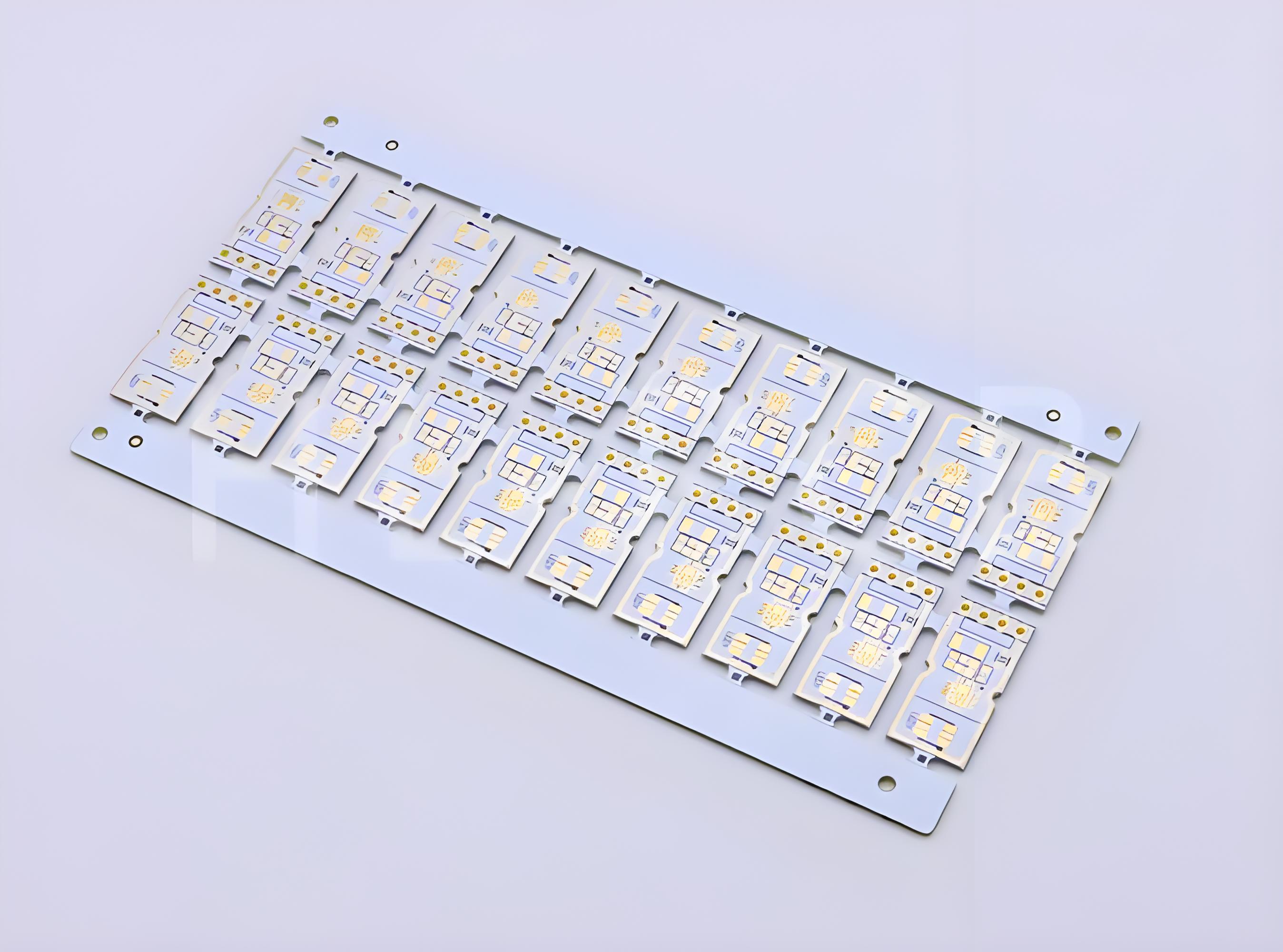
  • Solar energy systems
  • Laser modules and sensors

Whenever components get hot and space is tight, DTP copper MCPCBs offer a smart solution.

Tips for MCPCB Design with DTP Structure

Designing a DTP PCB requires special attention to thermal paths, layout, and material selection.

  1. Place heat-generating components directly over copper convexities
  2. Use high-conductivity dielectric materials to keep thermal resistance low
  3. Align thermal vias with component pads for effective heat flow
  4. Choose a suitable base material: aluminum for cost, copper for performance
  5. Ensure planarity and flatness for solid thermal contact

A carefully designed DTP MCPCB handles more power without compromising safety or reliability.

Why Is the Price of DTP MCPCB Higher Than a Normal MCPCB?

The cost of a DTP MCPCB is higher due to the complexity of its design and processing. It uses thicker copper or custom copper convexities, which are more expensive than standard copper foil. Creating a precise raised copper feature under each heat source requires extra machining steps, tight alignment, and rigorous quality checks.
Additionally, the dielectric materials used must have very high thermal conductivity and are usually more costly. The manufacturing process also involves advanced methods like X-ray alignment, CNC machining, and thermal performance testing. Despite the higher price, DTP MCPCBs offer long-term savings by improving thermal efficiency, reducing failure rates, and extending product lifespan.
How DTP MCPCBs Are Manufactured?

The manufacturing of a DTP MCPCB is more advanced than a standard MCPCB manufacturing process. It focuses on forming a raised copper boss (convexity) that provides a one-piece thermal bridge between the heat source and the metal base.

1. Base Metal Preparation

The aluminum or copper base is cleaned and pre-treated. This forms the foundation for the entire board.

2. Creating the Copper Convexity

A raised copper feature is formed on the base metal. This copper boss is placed directly beneath high-heat components. The convexity may be CNC machined or created during the copper plating process.

3. Dielectric Layer Lamination

A thin, high-thermal-conductivity dielectric is laminated around the copper convexity and onto the metal base. The copper bump remains exposed to make direct contact with the top copper circuit.

4. Copper Foil Application & Circuit Etching

Copper foil is laminated onto the surface and patterned using photolithography. The exposed part of the copper boss connects directly to a pad on the top layer.

5. Drilling & Plating (if required)

If the design includes signal vias or multi-layer connections, micro-drilling and copper plating are applied carefully to avoid damaging the copper boss.

6. Solder Mask & Surface Finish

Solder mask is printed, leaving heat transfer pads exposed. Surface finish (e.g., ENIG, HASL) is applied for soldering protection.

7. Inspection & Testing

  • X-ray confirms alignment of copper convexity under the pad
  • Thermal resistance is measured
  • Electrical continuity is tested
  • Visual and mechanical checks ensure no delamination or defects

This process requires tight process control and high-end fabrication equipment.

Benefits of Using DTP Copper MCPCB in High-Power Electronics

  • Superior thermal performance for high-wattage components
  • Longer component life due to reduced junction temperatures
  • Smaller form factor with higher power density
  • Stable performance under vibration, shock, and thermal cycling
  • Improved system efficiency and lower cooling requirements

These benefits make DTP MCPCBs an excellent investment for demanding applications.

What is DTP MCPCB? DTP Copper MCPCB Structure

DTP PCB Material Choices

A high-quality DTP PCB relies on the right materials:

  • Copper Convexity: Pure copper, usually 1–4mm thick
  • Dielectric Layer: Ceramic-filled epoxy or other high-conductivity material

Metal Base:

  • Aluminum: Lightweight, good for general use
  • Copper: Best thermal conductivity, ideal for extreme conditions

The right combination depends on your project needs, thermal limits, and cost targets.

Why Work With a Reliable DTP MCPCB Manufacturer?

Not all PCB manufacturers can build DTP MCPCBs. You need a supplier with tight process control, CNC machining, and advanced lamination tools.

A good DTP supplier should offer:

  • Custom DTP MCPCB design support
  • In-house thermal simulation and analysis
  • CNC or stamping for copper convexity
  • X-ray and AOI for high-precision quality control
  • Quick prototyping and scalable volume production

About Best Technology

At Best Technology, we are experts in DTP MCPCBs, aluminum PCBs, and thermal solution boards. We serve industries including LED, automotive, telecom, and medical electronics. We also use MES systems to provide full traceability of materials and processes. Our team can support you from design to mass production with reliable engineering and fast service.

Call To Action

If you’re working on a demanding project, contact Best Technology to learn how a custom DTP copper MCPCB can power your next innovation.

FAQs

1. What is a DTP MCPCB?

A Direct Thermal Path MCPCB uses a raised copper convexity to transfer heat directly from the component to the metal base.

2. How does a DTP copper MCPCB differ from a standard one?

It bypasses insulating layers by forming a direct copper path, reducing thermal resistance.

3. What are the main uses of DTP PCBs?

Used in LED lighting, power supplies, automotive electronics, and telecom base stations.

4. Why is the DTP MCPCB more expensive?

It uses more copper, complex machining, high-end materials, and tighter quality control.

5. Does Best Technology offer custom DTP MCPCB services?

Yes, we provide full engineering support, fast prototyping, and scalable production.

IMS PCB Full Form, Insulated Metal Substrate PCB Manufacturer
Tuesday, June 24th, 2025

IMS PCB full form is Insulated Metal Substrate PCB—a type of printed circuit board built to manage high heat and maintain strong mechanical support. It’s a popular choice for LED lighting, power supplies, and automotive electronics, where heat control is critical.

At Best Technology, we’re a trusted IMS PCB manufacturer in China, providing custom thermal management solutions with high precision, reliable materials, and a full range of engineering support. But let’s dig deeper into what makes insulated metal substrate PCBs unique—and why they’re so important in modern electronics.

IMS PCB Full Form, Insulated Metal Substrate PCB Manufacturer

What Is IMS Insulated Metal Substrate PCB?

An IMS (Insulated Metal Substrate) PCB is a type of circuit board that uses a thermally conductive dielectric layer bonded between a metal base (often aluminum or copper) and a copper circuit layer. The metal base helps dissipate heat more efficiently, especially compared to traditional FR4 boards.

When it comes to IMS PCB thermal conductivity, this is the most valuable feature. The dielectric layer in IMS boards typically offers a thermal conductivity range from 1.0 W/mK to over 8.0 W/mK, depending on the application. The metal base, like aluminum or copper, works as a built-in heat sink—pulling heat away from active components like LEDs, power transistors, or ICs. That’s why IMS PCBs are commonly used in LED modules, power converters, automotive lighting, and solar inverters—where both heat and performance need to be tightly controlled.

IMS PCB Material

Choosing the right material for an IMS board is essential. Three layers make up a standard IMS PCB: the metal base, the dielectric layer, and the copper foil. And for the metal base, there are two options: copper base and aluminum base.

  • Copper IMS PCB

Copper IMS PCBs offer superior heat transfer capabilities. Copper has a thermal conductivity of nearly 400 W/mK, much higher than aluminum. This means copper is ideal for applications with extreme power densities or where space is limited but heat is a concern.

However, copper is also more expensive and heavier than aluminum, so it’s generally reserved for high-performance needs like laser modules, RF circuits, or military-grade devices.

Copper IMS PCB
  • IMS Aluminum PCB

The IMS aluminum PCB is the most common choice. Aluminum provides good thermal conductivity (typically around 200 W/mK), excellent mechanical strength, and lower cost compared to copper.

Aluminum IMS PCBs are often used in LED lighting systems, electric vehicle chargers, power control modules, and industrial automation systems. They provide a balanced solution between cost and thermal management, which is why they’re the industry standard. Some common aluminum grades used include:

  • 5052 aluminum: Strong, corrosion-resistant, and suitable for structural use.
  • 6061 aluminum: Versatile, high-strength alloy.
  • 1060 aluminum: Excellent thermal conductivity, ideal for cost-sensitive applications.
IMS Aluminum PCB

IMS PCB Stackup

The stack-up of an IMS PCB refers to how the layers are arranged. A typical IMS PCB stackup includes:

  • Top copper trace layer – for routing signals and power.
  • Thermal dielectric layer – usually made of epoxy resin filled with ceramic for heat transfer.
  • Metal base – usually aluminum or copper.

For more advanced applications, 2 layer IMS PCBs are often used. In a 2 layer IMS PCB, an additional copper circuit layer is placed above the dielectric, and interconnections are formed using plated through-holes. These are useful when you need more complex routing or higher power density.

Multilayer IMS stackups are possible but require special lamination techniques. These are often customized depending on the mechanical, electrical, and thermal needs of the application.

IMS PCB Applications

Thanks to their excellent thermal performance and mechanical strength, IMS PCBs are widely used in demanding environments. Here are some key application areas:

  • LED lighting: Street lights, high-bay lights, grow lights, automotive headlights.
  • Power electronics: DC-DC converters, voltage regulators, motor drivers.
  • Automotive systems: Electric vehicle controllers, battery management units.
  • Industrial equipment: Robotics, welding machines, servo drivers.
  • Telecommunication: 5G base stations, power amplifiers.
  • Renewable energy: Solar panel inverters, wind turbine converters.

IMS PCB HS Codes

For companies that export or import IMS PCBs, understanding HS codes (Harmonized System codes) is essential for customs clearance and compliance.

The general HS Code for IMS PCB falls under:

8534.00 – Printed Circuits

Subcategories can vary depending on whether the board is populated (assembled) or bare.

To be more precise:

a. Bare IMS PCBs (unassembled):

  • HS Code 8534.00.90 (for 1-4 layer ims pcb)
  • HS Code 8534.00.10 (4 or above layer ims pcb)

b. Assembled IMS PCBs:

HS Code 8537.10 or others depending on final product classification and applications.

Always check with your local customs authority or logistics provider for the exact code applicable to your product type and destination country.

IMS PCB Assembly

IMS PCB assembly involves more care than standard FR4 boards due to thermal management and mechanical rigidity. Special attention must be given to soldering profiles and thermal expansion to prevent cracking or delamination.

Key points during assembly:

  • Use low-stress soldering methods (e.g., vapor phase or controlled reflow).
  • Ensure proper thermal profile during reflow to avoid damage to the metal base or insulation.
  • Choose high-Tg solder masks and components to handle high power density applications.

For high-volume needs, automated SMT lines should be optimized for heat dissipation and tight placement tolerances.

Best Technology offers one-stop IMS PCB assembly, including:

  • DFM (design for manufacturability) & DFA (design for assembly) checks
  • SMT and through-hole soldering
  • AOI, X-ray inspection
  • Functional testing
  • Box building assembly
  • Final inspection

Our strict quality control ensures your boards are built to meet thermal and mechanical demands.

Best IMS PCB Manufacturer – Best Technology

When choosing an IMS PCB manufacturer, experience, quality, and customization capabilities matter most. That’s where Best Technology stands out.

We specialize in insulated metal substrate PCBs with over a decade of industry focus. Our strength lies in advanced thermal management PCBs, from aluminum IMS boards to copper-core multilayer solutions.

Why Choose Best Technology for IMS PCBs?

✅ Technical Support Before & After Sales

✅ 99% Customer Satisfaction ISO9001, ISO13485, IATF16949, UL

✅ Material options: Wide range of metal bases (Al, Cu, Stainless Steel), dielectric materials with 1–8 W/mK.

✅ Full-stack service: From DFM support to final assembly and testing.

✅ MES traceability: Real-time tracking and control throughout production.

✅ Engineering support: Custom stackups, prototyping, thermal analysis, and layout review.

Whether you need a 2 layer IMS PCB for automotive lighting or a high-power copper IMS board for industrial drives, we can tailor the solution to fit your needs. With our strong supply chain and experienced team, we help customers worldwide bring their designs to life.

Best Technology is your go-to partner for custom IMS PCB fabrication and assembly. We combine deep technical knowledge, certified quality, and flexible manufacturing to deliver solutions that work—every time.

Ready to upgrade your thermal management? Contact Best Technology today for a quick quote or technical consultation.

FAQs

1. What is the difference between IMS PCB and FR4 PCB?

IMS PCBs use a metal base for better heat dissipation, while FR4 boards use fiberglass, which has low thermal conductivity.

2. Can IMS PCBs be multilayered?

Yes, multilayer IMS PCBs are possible but require special lamination techniques and are more complex to manufacture.

3. What are typical thermal conductivity values for IMS PCBs?

The dielectric layer in IMS boards usually ranges from 1 to 8 W/mK. Copper and aluminum also contribute to heat dissipation.

4. What is the HS code for an assembled IMS PCB?

Typically, 8537.10, but check with local customs authorities as codes can vary by region.

5. How can I request a custom IMS PCB quote from Best Technology?

Simply email us your Gerber files, BOM, and design requirements, or use our online quote form. Our engineers will get back to you quickly.

STM32H7B3I DK Development Boards
Monday, June 23rd, 2025

What is the STM32H7B3I DK PCB development board? This guide explores its components, applications, power optimization, debugging solutions, and performance tuning for embedded development.

As a leading manufacturer of STM32H7B3I DK PCB development boards, Best Technology delivers exceptional value through rapid prototyping and reliable production. Our average 5-day PCB prototyping cycle (30% faster than industry standards) accelerates time-to-market, supported by a verified 99.2% on-time delivery rate from our ISO-certified supply chain. Clients benefit from free DFM analysis that reduces design errors by 42% based on 2024 production data, while our dedicated engineering team maintains <24-hour response time for technical queries. With 15+ years of microcontroller board expertise, we maintain <0.8% defect rates across 10,000+ annual units produced. Our turnkey solutions include certified RoHS-compliant materials and full EMC/thermal testing documentation. Contact our sales team today for competitive quotes – 78% of new customers receive volume pricing discounts when requesting proposals through our online portal: sales@bestpcbs.com.

What Is STM32H7B3I DK PCB Development Boards?

The STM32H7B3I DK PCB development boards serves as a versatile platform for embedded system prototyping and evaluation, specifically tailored to harness the capabilities of its high-performance microcontroller. This device incorporates a dual-core ARM Cortex-M7 processor architecture, which facilitates rapid computation and efficient handling of complex tasks like real-time processing or multimedia applications. Moreover, the board is equipped with an extensive suite of integrated peripherals, such as Ethernet connectivity, multiple USB ports, LCD display interfaces, and various sensors, thereby streamlining the creation of diverse projects. Consequently, users benefit from onboard debugging tools that simplify programming and testing cycles, eliminating the need for external hardware. Ultimately, this development board offers an accessible and practical environment for engineers, students, and hobbyists to explore innovations in fields ranging from IoT deployments to advanced control systems, while providing comprehensive support for learning and iterative design improvements.

What Is STM32H7B3I DK PCB Development Boards?

What Are Components of STM32H7B3I DK PCB Development Boards?

Components of STM32H7B3I DK PCB development board:

  • Dual-Core Microcontroller Unit:‌ At the center of the board resides the dual-core processor, integrating a high-performance ARM Cortex-M7 core alongside an ARM Cortex-M4 core. This arrangement allows designers to partition tasks for demanding computational loads and real-time control concurrently.
  • External Memory Interfaces:‌ To support complex applications requiring substantial data storage or buffering, the board provides external memories. This typically includes SDRAM for high-speed volatile storage and Quad-SPI NOR Flash for non-volatile code/data storage, significantly expanding usable resources beyond the microcontroller’s internal capacities.
  • Integrated Power Management Circuitry:‌ Dedicated voltage regulators efficiently convert the main input power source (often USB or an external supply) into the multiple stable voltage levels necessary for the diverse components present, simplifying power setup and promoting reliable operation.
  • On-Board Debugger/Programmer:‌ A significant convenience feature is the embedded debug probe. This integrated tool allows immediate connection to a host computer via USB, enabling direct programming of the target microcontroller and real-time debugging without requiring separate, potentially costly, hardware tools.
  • Comprehensive Physical Connectivity:‌ The board incorporates numerous standard interfaces for peripheral connection and communication. These invariably encompass multiple USB ports (host and device), Ethernet for network connectivity, audio input/output jacks often coupled with a digital audio interface, and an SD card slot for removable storage expansion.
  • User Interaction Elements:‌ For immediate feedback and control during development, the board includes user LEDs, push-buttons, and potentially a reset button. Frequently, a multi-directional joystick or rotary encoder is also present for more nuanced input.
  • Display Interface:‌ Supporting embedded graphical user interfaces or visualization, a connector compatible with MIPI-DSI displays is typically included, enabling direct connection to compatible LCD panels or touchscreens.
  • Expansion Headers:‌ Crucially, extensive pin headers expose virtually all microcontroller I/O signals. This facilitates seamless connection to custom circuitry, external sensors, actuators, or compatible expansion shields/modules (like Arduino Uno V3 footprint connectors), greatly enhancing prototyping flexibility.
  • Potential Integrated Sensors:‌ Some versions might incorporate basic environmental sensors (like a digital microphone or temperature/humidity sensor) specifically included to provide immediate data sources for demonstration and initial application testing.
  • Audio Processing Components:‌ A dedicated audio codec chip is usually present to handle high-fidelity analog audio input and output conversion, interfacing directly with the microcontroller’s digital audio interfaces.
What Are Components of STM32H7B3I DK PCB Development Boards?

What Are Applications of STM32H7B3I DK PCB Evaluation Board?

Industrial Automation & Control

  • Programmable Logic Controllers (PLCs): Leverage the board’s multi-core ARM Cortex-M7/M4 processors to manage complex machinery, robotics, or conveyor systems with precise timing and I/O handling.
  • Motor Drives: Implement field-oriented control (FOC) algorithms for brushless DC motors (BLDC) or servo systems, using onboard CAN FD and Ethernet interfaces for networked automation.

Consumer Electronics & IoT

  • Smart Home Hubs: Develop gateways supporting Wi-Fi, Bluetooth Low Energy (BLE), and Thread protocols, utilizing the board’s cryptographic accelerators for secure device onboarding.
  • Wearable Tech: Optimize power consumption for fitness trackers or AR/VR devices via the board’s low-power modes and high-speed SPI/I2C interfaces for sensors.

Medical Devices

  • Portable Diagnostics: Create handheld ultrasound scanners or ECG monitors with the board’s dual-precision floating-point unit (FPU) for signal processing and TFT-LCD controller for on-device visualization.
  • Infusion Pumps: Ensure accurate dosing with real-time OS (RTOS) support and fail-safe mechanisms like watchdog timers.

Automotive Systems

  • In-Vehicle Infotainment (IVI): Drive high-resolution displays (up to 4K) and process audio/video streams using the board’s Chrom-ART graphics accelerator and HDMI-CEC support.
  • Advanced Driver-Assistance Systems (ADAS): Integrate radar/lidar data fusion with the board’s SDRAM interface and DMA controllers for low-latency decision-making.

Aerospace & Defense

  • Unmanned Aerial Vehicles (UAVs): Manage flight control, image processing, and telemetry with the board’s dual-bank Flash memory for over-the-air (OTA) firmware updates.
  • Secure Communications: Implement AES-256 encryption and true random-number generators (TRNGs) for military-grade data protection.

Research & Education

  • AI/ML Prototyping: Experiment with tinyML models using the board’s DSP instructions and external memory interfaces for edge inference tasks like image classification or anomaly detection.
  • Embedded Systems Courses: Teach real-time operating systems, low-power design, and hardware abstraction layers (HALs) with the board’s Arduino Uno V3-compatible headers.

How to Optimize Power Supply for STM32H7B3I-DK During Prototyping?

Use Low-Dropout (LDO) Regulators for Analog Peripherals

  • Power noise-sensitive modules (e.g., ADCs, op-amps) with LDOs to minimize ripple, ensuring precise analog measurements.
  • Pair with 10”F ceramic capacitors to filter high-frequency noise, critical for applications like medical diagnostics or audio processing.

Implement Dynamic Voltage Scaling (DVS)

  • Adjust the core voltage (VDD) between 1.8V–3.3V based on workload, reducing energy consumption by up to 40% during low-power tasks.
  • Lower VDD to 1.8V in Stop/Standby modes to extend battery life in portable devices.

Isolate High-Power Peripherals

  • Use separate regulators for USB-C, Ethernet, or displays to prevent current spikes from affecting the MCU’s stability.
  • Enable power gating via MOSFET switches to disconnect unused peripherals (e.g., SDRAM), cutting idle power by 20–30%.

Add Bulk Capacitance for Transient Loads

  • Place 100”F electrolytic capacitors near the VIN input to handle sudden current draws (e.g., motor startups), preventing voltage sags.
  • Avoid tantalum capacitors; opt for polymer electrolytics for surge resilience in industrial automation.

Leverage the Board’s Power Monitoring Features

  • Use the onboard INA226 current/power monitor to identify power hogs (e.g., USB OTG) and optimize their usage patterns.
  • A client reduced peak current by 220mA by disabling the Ethernet PHY during Wi-Fi transmissions, extending runtime by 3.2x.

Configure Low-Power Modes in Software

  • Shut down unused CPU cores and enable the RTC in Stop mode to maintain timestamps with <5”A consumption.
  • Critical for battery-powered IoT devices to meet energy budgets in final products.

Reduce Digital Switching Noise

  • Route high-speed signals (e.g., SDIO) away from analog power planes using the board’s multi-layer design.
  • Add ferrite beads between the MCU and noisy peripherals (e.g., CAN transceivers) to eliminate ADC noise-induced errors.

Optimize Power Sequencing

  • Follow STM32’s recommended startup sequence (VDD → VDDA → VREF+) to avoid latch-up or data corruption.
  • Use the board’s power-on-reset (POR) circuit to ensure consistent startup states, reducing debugging time by 50%.

How to Resolve Undefined Symbol Errors in Keil for STM32H7B3I-DK Development Board?

Here’s a structured troubleshooting guide to resolve undefined symbol errors in Keil for the STM32H7B3I-DK board, designed to save time and reduce frustration:

1. Verify Library and File Inclusion‌

  • Ensure all necessary firmware libraries (e.g., HAL/LL drivers) are added to the project.
  • Confirm header file paths are correctly configured in the IDE’s project settings.
  • Check if source files (.c) containing the missing functions are included in the build.

2. Inspect Linker Configuration‌

  • Review the linker script (.sct/.ld) to confirm memory regions align with the MCU’s specifications.
  • Validate startup files (e.g., startup_stm32h7b3.s) are present and match the MCU model.

3. Resolve Dependency Chains‌

  • If using external modules (Wi-Fi, displays), ensure their libraries are linked and compatible with the MCU core.
  • Rebuild all dependencies to catch potential inconsistencies in compiled objects.

4. Check Compiler Definitions‌

  • Preprocessor macros (e.g., USE_HAL_DRIVER) must be defined in the IDE’s global settings.
  • Verify target MCU definitions (e.g., STM32H7B3xx) are active.

5. Address Common Pitfalls‌

  • C/C++ Mixing‌: Avoid calling C++ functions from C files without extern “C” wrappers.
  • Optimization Conflicts‌: Temporarily disable compiler optimizations to isolate issues.

6. Systematic Debugging‌

  • Clean and rebuild the project to force fresh compilation.
  • Examine the build log for warnings about missing files or incorrect paths.

What Causes Data Corruption During SPI DMA Transfers on STM32H7B3I-DK?

Here are common causes of data corruption during SPI DMA transfers on the STM32H7B3I-DK board:

  • Clock Synchronization Issues‌: Mismatched clock speeds between the SPI peripheral and DMA controller can lead to timing violations, causing missed or duplicated data bits during transfers.
  • Buffer Alignment Problems‌: Improperly aligned memory buffers (not matching the DMA’s address requirements) may result in partial writes or reads, corrupting adjacent memory locations.
  • Concurrent Memory Access Conflicts‌: If the CPU or other peripherals access the same memory region during DMA operations, bus contention occurs, potentially overwriting or reading stale data.
  • Incorrect DMA Configuration‌: Misconfigured transfer modes (e.g., circular vs. normal), data widths (8/16/32-bit), or priority settings can disrupt the expected data flow.
  • SPI Protocol Violations‌: Improperly timed chip-select signals, clock polarity/phase mismatches, or noise on physical lines may corrupt bits mid-transmission.
  • Interrupt Handling Delays‌: High-priority interrupts delaying DMA ISR execution might cause buffer overflows or underflows if not properly managed.
  • Power Supply Noise‌: Voltage fluctuations during transfers can introduce bit errors, especially in high-speed SPI modes where signal integrity is crucial.
  • Cache Coherency Oversights‌: When using cached memory regions without proper maintenance (clean/invalidate operations), stale cache entries may be read instead of fresh DMA data.
  • Hardware FIFO Overruns‌: SPI peripheral FIFO buffers overflowing due to delayed DMA servicing can drop data or mix old/new bytes.
  • Software Race Conditions‌: Prematurely modifying DMA descriptors or control registers while transfers are active may halt operations mid-cycle.
What Causes Data Corruption During SPI DMA Transfers on STM32H7B3I-DK?

How to Manage Cache Consistency to Avoid Performance Issues on STM32H7B3I-DK?

Here are practical methods to manage cache consistency and prevent performance degradation on the STM32H7B3I-DK, with actionable solutions:

Explicit Cache Maintenance for DMA Buffers‌

  • Before starting DMA transfers, invalidate the cache for the receive buffer to ensure fresh data is fetched from memory.
  • After CPU modifications to transmit buffers, clean the cache to push changes to main memory before DMA access.
  • Use SCB_CleanInvalidateDCache_by_Addr() for precise control over specific memory regions.

Memory Attribute Configuration‌

  • Mark DMA buffers as non-cacheable or write-through in the MPU (Memory Protection Unit) settings to bypass cache for critical data paths.
  • Allocate buffers in non-cacheable memory regions (e.g., SRAM4) when deterministic timing is required.

Cache Coherency with Double Buffering‌

  • Implement dual-buffering: While DMA writes to one buffer, the CPU processes data from the other, separated by cache-line-aligned addresses.
  • Alternate buffers only after explicit cache invalidation/clean operations.

Synchronization Barriers‌

  • Insert __DSB() (Data Synchronization Barrier) after cache operations to ensure completion before subsequent instructions execute.

DMA Descriptor Placement‌

  • Store DMA descriptors in non-cacheable memory or use attribute((section(“.noncache”))) to prevent stale descriptor reads.

Interrupt-Driven Cache Management‌

  • In DMA completion ISRs, invalidate caches before processing received data and clean caches before initiating new transfers.

Monitoring Cache Hits/Misses‌

  • Use performance counters (if available) to identify excessive cache misses, indicating suboptimal buffer alignment or size.

Compiler Directives for Alignment‌

  • Enforce cache-line alignment (e.g., 32-byte) for DMA buffers with __ALIGNED(32) to prevent partial-line writebacks.

Write-Back vs. Write-Through Policy Selection‌

  • Configure write-back mode for CPU-intensive tasks but switch to write-through for shared DMA buffers to reduce coherency overhead.

Debugging Aids‌

  • Enable cache error interrupts and use breakpoints to verify cache states during transfers.
  • Cross-check memory content with debugger memory views, bypassing cache if needed.

Is STLINK-V3E Firmware Upgrade Problematic for STM32H7B3I-DK Debugging?

Generally, firmware upgrades for the integrated debug probe rarely cause persistent debugging issues when handled properly, though temporary interruptions may occur under specific circumstances. Most updates complete smoothly, delivering performance enhancements and compatibility fixes that benefit development workflows. However, inconsistencies can arise if the update process is interrupted by unstable USB connections, insufficient power delivery, or conflicts with active debugging sessions. Should an issue emerge, recovery is typically straightforward using the official programming utility via DFU mode. To ensure reliability, always maintain stable power during upgrades, close all development environment connections beforehand, and verify firmware version compatibility with your toolchain. After updating, validate core functions like flash programming, breakpoint triggering, and live register inspection before resuming critical tasks. Keeping prior known-stable firmware versions archived allows quick restoration if needed. Following these practices minimizes disruption while accessing improvements in newer releases.

CCPD XR495 007 V4.0 Panel PCB
Thursday, June 19th, 2025

What makes CCPD XR495 007 V4.0 panel PCB stand out in LED applications? This guide covers configurations, thermal management, soldering, and reliability solutions.

At Best Technology, we manufacture premium CCPD XR495 007 V4.0 panel PCBs and other metal core PCB with industry-leading capabilities that directly benefit your projects. Our advanced manufacturing process delivers 30% faster turnaround than competitors, helping you meet critical deadlines. Whether you need mass production or just one prototype for testing, we offer the same high-quality standards with no minimum order requirements. We maintain complete pricing transparency – you’ll never encounter hidden fees or unexpected charges. Our engineering team provides free DFM analysis to optimize your designs for performance and cost-efficiency. With IPC Class 3 certified production, automated optical inspection, and strict quality control, we guarantee reliable PCBs that outperform industry standards. Specializing in thermal management solutions for LED applications, our CCPD XR495 007 V4.0 panel PCBs feature superior heat dissipation and uniform brightness control. From automotive to industrial applications, we deliver robust solutions tailored to your exact specifications. Get a competitive quote today and experience the Best Technology difference – where quality, speed and affordability meet. Contact our sales team now to discuss your project requirements: sales@bestpcbs.com.

What Is CCPD XR495 007 V4.0 Panel PCB?

The CCPD XR495 007 V4.0 panel PCB represents an advanced iteration of panel PCB technology designed for high-performance applications. This version integrates enhanced thermal management and signal integrity features, making the CCPD XR495 007 V4.0 panel PCB particularly suitable for multilayer designs requiring consistent impedance control. With improved copper balancing and solder mask adhesion, the CCPD XR495 007 V4.0 panel PCB ensures reliable performance across extended operating cycles while maintaining compatibility with lead-free assembly processes. The design refinements in this iteration address common challenges in panelized PCB production, including warpage prevention and via reliability. Engineers working with high-density interconnects will find the material properties and manufacturing tolerances of CCPD XR495 007 V4.0 panel PCB adapted for precision applications where dimensional stability matters. Its standardized panelization approach simplifies fabrication while optimizing material utilization during mass production.

CCPD XR495 007 V4.0

What Are Configurations of CCPD XR495 007 V4.0 Panel PCB?

Here are the configurations of CCPD XR495 007 V4.0 panel PCB:

  • Layer Stackup Options‌: This panel PCB supports configurations from 8 to 24 conductive layers, with sequential lamination for high-density interconnects. Standard builds incorporate FR-4 Tg170 core materials complemented by low-loss prepregs optimized for signal integrity.
  • Copper Weight Specifications‌: Available in 1oz to 4oz finished copper weights per layer. Heavy copper editions enable 40A continuous current handling on power planes while finer 0.5oz copper supports controlled impedance signal layers.
  • Surface Finish Variants‌: Multiple finishing processes include ENIG (Electroless Nickel Immersion Gold) for fine-pitch components, immersion silver for RF applications, and HASL-LF for cost-effective solutions. Each finish undergoes rigorous solderability testing.
  • Thermal Management Builds‌: Aluminum-core configurations feature thermally conductive dielectric layers, achieving 1.2°C/W thermal resistance. These specialized CCPD XR495 007 V4.0 panel PCB editions effectively dissipate heat from power components.
  • Panelization Formats‌: Standard panels measure 18″x24″ with breakout tabs or 21″x24″ for V-score separation. Custom panel designs accommodate specific assembly fixtures, particularly for automotive radar modules requiring precise component placement.
  • High-Frequency Material Integration‌: Hybrid constructions pair standard FR-4 with Rogers 4350B laminates in critical RF sections. This CCPD XR495 007 V4.0 panel PCB approach maintains stable Dk values (±0.05) across 5-77GHz frequency ranges.
  • Specialty Thickness Profiles‌: Final board thickness ranges from 0.8mm for wearable devices to 3.2mm for industrial power converters. All configurations maintain consistent dielectric spacing tolerances within ±8%.
  • Protection and Coating‌: Optional conformal coatings include acrylic for general use, silicone for high-temperature environments, and parylene for medical implants. Edge plating configurations provide additional corrosion resistance.
CCPD XR495 007 V4.0

What Are Applications of CCPD XR495 007 V4.0 Panel PCB?

Here are the primary applications for CCPD XR495 007 V4.0 panel PCB:

  • Telecommunications Infrastructure: The CCPD XR495 007 V4.0 panel PCB enables stable 5G millimeter-wave circuits due to its impedance-controlled dielectric layers. Base stations deploy these panels for beamforming antenna arrays where signal integrity above 24GHz becomes essential.
  • Industrial Power Electronics: Motor controllers and uninterruptible power supplies benefit from this PCB’s thick copper variants. Specifically, CCPD XR495 007 V4.0 panel PCB configurations tolerate sustained 150A surges while maintaining thermal stability through rapid cycling events.
  • Medical Diagnostic Systems: Advanced imaging equipment utilizes this standard for low-noise sensor interfaces. The microvia technology within CCPD XR495 007 V4.0 isolates sensitive analog components from digital interference in MRI machines and digital X-ray detectors.
  • Automotive Control Units: Electric vehicle power management modules implement this panel PCB for vibration resistance. Its thermal cycling endurance ensures reliable operation in battery management systems exposed to -40°C to 160°C temperature swings.
  • Aerospace Avionics: Flight control systems require the certified material traceability inherent in this standard. Furthermore, CCPD XR495 007 V4.0 panel PCB assemblies pass rigorous altitude testing for cabin pressure instrumentation without dielectric breakdown.
  • High-Intensity Lighting Systems: Thermal management editions with metal cores manage 200W+ LED clusters efficiently. These specialized CCPD XR495 007 V4.0 versions maintain junction temperatures below 85°C in stadium lighting arrays.
  • Robotics Motion Hardware: Multi-axis controllers leverage the 24-layer configurations for distributed processing. The panelization scheme provides necessary rigidity during high-G maneuvers while preserving signal timing across servo networks.

How to Manage Heat Dissipation in CCPD XR495 007 V4.0 Panel PCB Design?

Optimized heat dissipation strategies for CCPD XR495 007 V4.0 panel PCB design:

  • Component Placement: Spread high-power components (e.g., voltage regulators, power transistors) evenly to avoid localized heating on the CCPD XR495 007 V4.0 panel PCB. Keep heat-sensitive parts (e.g., analog sensors) isolated to prevent thermal interference.
  • Thermal Vias: Add dense thermal via arrays under heat sources to conduct heat to inner copper layers. Use 0.3mm vias with 0.5mm spacing for efficient vertical cooling without signal integrity issues.
  • Copper Pour Expansion: Increase copper areas near hot components to spread heat laterally. Connect these zones to heat spreaders or chassis points using thermal interface materials to reduce peak temperatures.
  • Material Selection: Choose substrates like aluminum-backed FR4 or ceramic-filled laminates for better thermal conductivity. Pair with low-resistance solder masks to avoid insulating heat on the PCB surface.
  • Airflow Channels: Design trace routes to create airflow paths aligned with fans or natural convection. Avoid blocking ventilation zones with components in enclosed systems.
  • Thermal Simulation: Use CFD tools to model heat distribution on the CCPD XR495 007 V4.0 panel PCB under extreme loads. Validate with infrared imaging and adjust layouts based on test results.
  • Power Domain Isolation: Separate high-current and low-power sections using guard traces and ground planes. This minimizes thermal crosstalk and improves signal stability.
  • Component Packages: Select SMD packages with exposed thermal pads or heat slugs. Ensure direct contact with copper pours for efficient conductive cooling.

How to Achieve Uniform Light Brightness For Multi-Color CCPD XR495 007 V4.0 Panel PCB?

 Below are actionable strategies to optimize brightness uniformity of multi-color CCPD XR495 007 V4.0:

  • LED Binning and Selection – Partner with suppliers to source LEDs from the same brightness and color bin. This minimizes inherent variations in luminous intensity and chromaticity, ensuring each LED on the CCPD XR495 007 V4.0 panel PCB performs identically. Doing so reduces the need for excessive post-production calibration and guarantees visual consistency.
  • Current Matching Circuit Design – Implement precision current regulators for each LED channel. By maintaining identical current levels across all LEDs, you prevent overdriving some pixels while underpowering others. This approach extends LED lifespan and preserves brightness consistency, even as the CCPD XR495 007 V4.0 panel PCB ages.
  • Optimized PCB Layout – Arrange LEDs in a staggered or matrix pattern to blend colors evenly. Avoid clustering LEDs of the same hue, as this creates visible “hotspots” or color tints. A well-planned layout ensures smooth color transitions and eliminates perceptible brightness variations.
  • Diffuser and Light Guide Integration – Incorporate optical-grade diffusers or light guide plates (LGPs) above the LED array. These components scatter light uniformly, masking minor LED discrepancies and creating a cohesive visual output. For the CCPD XR495 007 V4.0 panel PCB, this step is particularly effective in eliminating angular brightness deviations.
  • Thermal Management Synergy – Leverage the PCB’s thermal dissipation design to maintain stable operating temperatures. Uneven heating can cause LEDs to drift in brightness or color over time. By integrating heat-spreading copper pours and thermal vias, you ensure all LEDs perform within their optimal temperature range, preserving long-term uniformity.
  • Pre-Production Calibration – Conduct individual pixel-level brightness calibration during manufacturing. Use spectroradiometers to measure and adjust each LED’s output, compensating for minor variations. This process guarantees the CCPD XR495 007 V4.0 panel PCB meets strict brightness uniformity standards before deployment.
  • Aging and Drift Compensation – Include firmware that dynamically adjusts LED drive currents based on real-time performance data. This compensates for gradual brightness decay or color shifts, ensuring the CCPD XR495 007 V4.0 panel PCB maintains visual consistency throughout its service life.
  • Environmental Robustness Testing – Validate the design under extreme temperatures, humidity, and voltage fluctuations. Identify and rectify conditions that cause uneven brightness degradation, ensuring reliable performance in diverse real-world scenarios.
CCPD XR495 007 V4.0 Panel PCB

How to Choose the Best Surface Finish For Reliable LED PCB Soldering?

  • Evaluate Environmental Exposure: If the CCPD XR495 007 V4.0 panel PCB will operate in humid, corrosive, or high-temperature environments, prioritize finishes like ENIG (Electroless Nickel Immersion Gold) or ENEPIG (Electroless Nickel Electroless Palladium Immersion Gold). These offer superior corrosion resistance and prevent oxidation-related soldering issues.
  • Consider LED Pitch and Density: For fine-pitch LED arrays, choose finishes with exceptional planarity, such as Immersion Silver or OSP (Organic Solderability Preservatives). These minimize solder bridging and ensure consistent wetting across closely spaced pads on the CCPD XR495 007 V4.0 panel PCB.
  • Assess Long-Term Reliability Needs: Applications requiring 10+ years of service life benefit from ENIG or ENEPIG, which resist tarnishing and maintain solderability over time. Avoid HASL (Hot Air Solder Leveling) for LED PCBs, as its uneven surfaces may compromise fine-pitch solder joints.
  • Balance Cost and Performance: For cost-sensitive projects, Immersion Tin or OSP provide acceptable performance at lower prices. However, note that OSP has a shorter shelf life and requires strict humidity control during storage to prevent degradation.
  • Test for Thermal Cycle Resistance: LED PCBs often endure repeated thermal expansion. ENEPIG excels here due to its palladium barrier layer, which prevents nickel corrosion during thermal cycling. This finish is ideal for the CCPD XR495 007 V4.0 panel PCB in applications with frequent on/off cycles.
  • Verify Compatibility with Lead-Free Soldering: If using lead-free processes, opt for Immersion Silver or ENIG. These finishes withstand the higher reflow temperatures required for lead-free alloys without degrading solder joint integrity.
  • Address Signal Integrity Requirements: For LED PCBs with high-speed data lines, Immersion Silver offers a flat, conductive surface that minimizes signal loss. Avoid finishes like HASL, which can introduce uneven surfaces and impedance discontinuities.
  • Consult with Your Contract Manufacturer: Work closely with your PCB fabricator to validate finish selection. They can provide samples of the CCPD XR495 007 V4.0 panel PCB with different finishes for solderability testing, ensuring alignment with your production equipment and processes.

What Causes Soldering Defects in CCPD XR495 007 V4.0 Panel PCB Assembly?

Solder Bridging Between Pads

  • Cause: Excess solder paste or misaligned stencils create unintended electrical connections.
  • Solution: Optimize stencil thickness and aperture design for the CCPD XR495 007 V4.0 panel PCB’s pad geometry. Use laser-cut stainless-steel stencils with electropolished finishes to reduce paste bleed.

Cold or Incomplete Joints

  • Cause: Inadequate reflow heating prevents proper solder fusion, leaving weak joints.
  • Solution: Calibrate reflow ovens to match the FR4 substrate’s thermal profile. Ensure the peak temperature aligns with the solder alloy’s melting range while avoiding overheating.

Tombstoning of LED Components

  • Cause: Uneven solder paste deposition or imbalanced pad finishes cause components to lift during reflow.
  • Solution: Standardize pad finishes (e.g., ENIG) across the CCPD XR495 007 V4.0 panel PCB and verify stencil alignment using automated optical inspection (AOI).

Pad Lifting or Delamination

  • Cause: Excessive mechanical stress or thermal shock damages the FR4 Copper Clad Circuit Board’s adhesion.
  • Solution: Reduce pick-and-place forces and optimize reflow ramp rates. For thick boards, use preheating to minimize thermal gradients.

Solder Balling or Splatter

  • Cause: Contaminated flux or poor preheat settings cause volatile outgassing during soldering.
  • Solution: Store FR4 boards in dry conditions and use high-quality no-clean fluxes. Increase preheat temperatures to 90–110°C to evaporate moisture before reflow.

Component Misalignment

  • Cause: Incorrect placement speed or nozzle pressure shifts components during assembly.
  • Solution: Adjust pick-and-place parameters for the CCPD XR495 007 V4.0 panel PCB’s component density. Use vacuum calibration tools to ensure accurate pickup.

Oxidized Solder Joints

  • Cause: Exposure to humidity or outdated solder paste degrades solderability.
  • Solution: Use nitrogen-inerted reflow ovens to minimize oxidation. Store solder paste in airtight containers and follow FIFO (first-in, first-out) protocols.

Inconsistent Solder Filets

  • Cause: Uneven pad copper weights or improper solder mask alignment disrupt wetting.
  • Solution: Standardize copper weights across the FR4 board and validate solder mask registration using electrical test coupons.

How to Avoid CCPD XR495 007 V4.0 Panel PCB Damage During PCB Bending?

  • Optimize Board Stack-Up Design: Reinforce the PCB with a balanced layer stack-up, incorporating core layers with high glass transition temperature (Tg) materials. For the CCPD XR495 007 V4.0 panel PCB, use a 4–6 layer design with symmetrical copper distribution to resist flexing forces.
  • Incorporate Stiffeners Strategically: Attach FR4 or aluminum stiffeners to high-stress zones, such as connector edges or mounting points. These add structural rigidity without adding excessive weight, protecting the PCB from bending-induced fractures.
  • Use Flex-Rigid Hybrid Technology: For applications requiring repeated flexing, adopt a flex-rigid PCB design. This combines rigid FR4 sections with flexible polyimide zones, allowing controlled bending while isolating sensitive components on the CCPD XR495 007 V4.0 panel PCB from stress.
  • Minimize Trace Tension: Route traces perpendicular to anticipated bending axes to reduce peel-off risks. Widen traces in high-flex areas and avoid sharp 90° angles, which concentrate stress.
  • Select High-Tg Laminates: Choose PCB materials with Tg ≄ 170°C, such as IS410 or IT180A, to resist deformation under mechanical stress. These laminates maintain dimensional stability during bending, protecting solder joints and plated-through holes (PTHs) on the CCPD XR495 007 V4.0 panel PCB.
  • Implement Component-Side SMT Restrictions: Avoid placing tall or heavy components on the side exposed to bending forces. Mount fragile parts (e.g., BGAs, QFNs) on the opposite side or use underfill adhesives to anchor them.
  • Control Panelization and Depanelization: Use V-score or routed breakaway tabs with sufficient remaining web width (≄0.5mm) to prevent premature board separation. Depanelize boards with a scoring machine to avoid torsional stress during singulation.
  • Validate with Stress Testing: Subject prototypes to cyclic bending tests (e.g., 1,000 cycles at ±5mm deflection) using a universal testing machine. Analyze failures with cross-sectional microscopy and refine the design iteratively.

Conclusion

The CCPD XR495 007 V4.0 Panel PCB is a high-performance solution for advanced LED applications, offering versatile configurations, robust thermal management, and uniform multi-color brightness. This article explores its technical specifications, industrial uses, and assembly best practices, including surface finish selection and defect prevention. Whether you need optimized heat dissipation or bend-resistant designs, this PCB delivers reliability across demanding environments. For competitive pricing and expert support, contact Best Technology now: sales@bestpcbs.com.

RGBW LED Swimming Pool Light Aluminum PCB Manufacturer
Tuesday, June 17th, 2025

Swimming pool light aluminum PCBs are key to reliable and efficient underwater lighting. With RGBW LEDs becoming more popular, these boards must manage heat, moisture, and high brightness. In this guide, we’ll cover the basics of swimming pool light PCBs, compare RGBW vs. regular designs, explain why aluminum PCB is preferred, and show how Best Technology supports your lighting projects with expert manufacturing.

What is Swimming Pool Light PCB?

A swimming pool light PCB is the printed circuit board that powers and connects the components inside waterproof pool lighting fixtures. These lights are submerged in water and must operate safely and efficiently. The PCB controls the illumination—typically in RGB or RGBW color modes—and manages heat and power in demanding underwater environments.

Choosing the right PCB material, design, and layout is critical to ensure long service life and consistent brightness. Because water exposure, thermal load, and sealing requirements are significant, most pool lighting PCBs are built using aluminum PCB substrates.

RGBW LED Swimming Pool Light Aluminum PCB Manufacturer

Regular vs. RGBW LED Swimming Pool Light PCB

When we compare standard pool light PCBs to RGBW LED swimming pool light PCBs, the difference lies in color quality, thermal management, and complexity.

Regular PCBs use RGB LEDs (Red, Green, Blue), which create color mixes but lack dedicated white light. This can limit brightness and clarity in larger pools or color-changing sequences.

RGBW LED PCBs, on the other hand, add a true white LED. This provides:

  • Better color accuracy
  • Enhanced brightness
  • More realistic lighting for ambiance

Since RGBW LEDs generate more heat and require more current paths, they demand better thermal control. That’s where aluminum PCB steps in—offering a reliable base to dissipate heat and maintain performance.

RGBW LED Swimming Pool Light Aluminum PCB Manufacturer

Full Design Guide to Swimming Pool Light PCB

Designing a swimming pool light aluminum PCB requires a balance between thermal performance, mechanical strength, and compact layout. Here’s a step-by-step guide to get it right:

1. Choose the Right Aluminum Core

Start with selecting an appropriate aluminum base (typically 1.0–2.0 mm thickness). It should have:

  • Good thermal conductivity (usually 1.0–3.0 W/m·K)
  • Electrical insulation between layers
  • Surface flatness for LED mounting

2. Select High-Brightness RGBW LEDs

Pick LEDs designed for underwater use. They should:

  • Operate at low voltage (12V or 24V)
  • Have IP68 or similar sealing ratings
  • Be thermally efficient

3. Layout for Symmetrical Light Distribution

The LED layout must ensure even light spread, avoiding hot spots or shadow zones. Circular or star-shaped layouts are common in pool lighting PCBs.

4. Optimize Thermal Vias and Heat Flow

Even with an aluminum base, thermal vias help move heat from the LED pads to the metal core. Use large copper pours and direct thermal paths.

5. Surface Finishing for LED Pads

Use ENIG or OSP surface finishes to prevent oxidation and enhance solderability. These finishes are RoHS-compliant and work well with SMT LEDs.

6. Solder Mask and Silkscreen

The solder mask should withstand UV exposure and chlorinated water. White or blue masks are common for aesthetic reasons.

7. Waterproofing and Final Assembly

The PCB must integrate into a waterproof enclosure, often with potting compounds or silicone gaskets. Conformal coating adds extra protection.

Why Not Choose Copper as Swimming Pool Light PCB Base?

Many people ask: Why not just use copper PCBs for pool lights? Isn’t copper more conductive? While copper indeed has better conductivity, it’s not always the right choice here. Let’s break down why:

  • Cost-Effective

Copper-core PCBs are expensive due to the material cost and processing complexity. In contrast, aluminum PCBs are much more budget-friendly, especially for large lighting projects.

  • Weight

Aluminum is lighter than copper. In underwater lighting, every gram matters for mounting and buoyancy. Using aluminum reduces the overall system weight, making handling and installation easier.

  • Delivery Time

Aluminum PCBs are faster to fabricate and assemble, so it can save much time for customers to win the market. Manufacturers like Best Technology can offer quicker lead times with stable quality, making project deadlines easier to meet.

Swimming Pool Light RGBW LED Aluminum PCB Price

The cost of a RGBW LED swimming pool light aluminum PCB depends on several key factors:

FeatureImpact on Price
Board SizeLarger boards use more aluminum and increase cost
LED DensityMore RGBW LEDs mean tighter layout and more layers
Thermal ConductivityHigher W/m·K rating substrates cost more
Surface FinishENIG is more expensive than OSP or HASL
Thickness1.6mm boards are cheaper than 2.0mm or thicker
Order QuantityHigher volume reduces per-unit cost
AssemblySMT components add cost depending on complexity

On average, a single-layer aluminum PCB for RGBW pool lights ranges from $0.80 to $2.50 per piece in medium volumes. Double-layer boards may go up to $4.00 or more, depending on features.

Your Best Swimming Pool Light Solution Provider – Best Technology

When you’re looking for a trusted swimming pool light aluminum PCB manufacturer, you need more than just low prices. You need:

  • Precise engineering
  • Fast turnaround
  • High quality and consistency
  • Responsive service

That’s where Best Technology shines. We specialize in LED aluminum PCB manufacturing, with tailored solutions for RGBW lighting applications in harsh environments like swimming pools.

We support:

  • Custom thermal designs
  • PCB + PCBA service
  • UV-resistant materials
  • RoHS & REACH compliance
  • Rapid prototyping to mass production

Our team works closely with lighting brands, OEMs, and system integrators to deliver high-reliability pool lighting PCBs on time and within budget.

Our Aluminum PCB & PCBA Process Capability

Best Technology is not only a PCB manufacturer—we also offer full PCBA (PCB assembly) services. Our capabilities include:

ItemCapability
PCB Layers1 to 10 layers for aluminum PCB
Board Thickness0.4mm to 3.2mm
Max Board Dimension610*1625mm
Conductor Thickness0.5oz-10oz
Min Line Width/Line Space4/4mil
Min Solder Mask Bridge8mil
Thermal ConductivityUp to 3.0 W/m·K
Surface FinishENIG, OSP, HASL, Imm Silver, Imm Tin
Solder Mask ColorWhite, Black, Green (others are available)
Component Placement01005, QFN, BGA
Assembly TypeSMT, Through-hole, Hybrid
TestingAOI, X-ray, ICT, Functional Testing

FAQs

Q1: What’s the difference between RGB and RGBW in pool lighting PCBs?

RGB uses three LEDs to create colors, while RGBW adds a dedicated white LED, offering better clarity and light balance underwater.

Q2: Can aluminum PCBs handle the heat from high-power LEDs?

Yes. With a good layout and high thermal conductivity aluminum, these PCBs effectively dissipate heat from RGBW LEDs.

Q3: How long does it take to manufacture swimming pool light aluminum PCBs?

Standard lead time is 3–5 working days for bare PCBs, and 5–7 working days for PCB + assembly, depending on complexity. Expedited service available for aluminum PCB.

Q4: Can Best Technology help with LED selection and layout optimization?

Absolutely. Our engineering team offers DFM (Design for Manufacturability) reviews, LED sourcing, and thermal simulations.

Q5: Do aluminum PCBs support double-sided assembly?

While aluminum PCBs are mainly single-sided, hybrid double-layer designs are possible with proper insulation and structure.

Want to bring your RGBW swimming pool light project to life with the right aluminum PCB?

Contact Best Technology today—we’ll help you build efficient, cost-effective, and beautiful underwater lighting systems. If you want to copper metal core PCB fabrications, we are also here.

High-quality PCB Contract Manufacturing Service
Thursday, June 5th, 2025

What Is PCB Contract Manufacturing?

PCB contract manufacturing is a process where companies outsource the production of printed circuit boards to a third-party manufacturer. This includes not just making the board, but also assembling components, running functional tests, and sometimes even final product packaging. It allows companies to focus on core tasks like product development and marketing, while the technical side of electronics production is handled by experts.

At its core, PCB contract manufacturing saves time, reduces production costs, and ensures consistency in quality. For startups and global electronics brands alike, finding a dependable contract manufacturer can significantly boost speed-to-market and reduce project risks.

High-quality PCB Contract Manufacturing Service

Our Printed Circuit Board Services

At Best Technology, we offer a complete range of services under one roof. Whether you’re developing a new electronic product or scaling up production, we handle everything from the initial design to final functional testing. Here’s what we bring to the table:

  • PCB Layout & Design

We help you start from scratch or improve your existing Gerber files. Our layout team is experienced in high-density routing, impedance control, and EMC-compliant designs. With tools like Altium Designer and CAD, we ensure accurate and efficient PCB layouts tailored to your project needs.

  • OEM & ODM PCB Manufacturing

Whether you need OEM or ODM service, we have the capability to take your concept and turn it into a working product. Our engineering team collaborates closely with clients to deliver custom solutions that are production-ready.

  • Electronic Components Assembly

From SMT (Surface Mount Technology) to through-hole assembly, our facility is equipped for full-scale PCBA (Printed Circuit Board Assembly). We support both leaded and RoHS-compliant assembly and offer automated inspection (AOI), X-ray, and BGA rework services to guarantee every joint is solid and reliable.

  • Wire Harness Assembly

We also supply PVC/PE/TPU/LZSH hook-up wire, flat cable, connector wire harness for machinery equipment, and cables for the field of electronic appliances, DC power supply, audio video devices, toys, medical equipment, communication devices, electrician & electrical, computer accessories cable, and so on.

  • Box Building Assembly

We don’t stop at the board level. If you need enclosure integration, cable harnessing, or full unit assembly, our box building assembly service is available. This end-to-end solution simplifies your supply chain and gives you more control over the finished product.

  • Functional Testing

We provide full functional testing based on your test procedure or help you develop one. This includes power-on tests, signal integrity verification, and custom fixture testing. We ensure your board works perfectly before it reaches your customers.

High-quality PCB Contract Manufacturing Service

What PCBs We Can Fabricate?

Our team at Best Technology specializes in a wide range of printed circuit board types. No matter your project’s complexity or environment, we’ve got you covered. Here are some products that we can make, but not limited to these PCBs.

  • Extra Thin PCB

For devices that require tight packaging like smart cards, cameras, or medical sensors, we offer ultra-thin PCBs as thin as 0.1mm. These boards maintain strength while saving space.

  • HDI PCB

High-Density Interconnect (HDI) PCBs support advanced electronics with fine-pitch components, blind and buried vias, and micro-via-in-pad technology. These are perfect for smartphones, tablets, and compact IoT devices.

  • RF PCB

We manufacture RF (Radio Frequency) PCBs using low-loss materials like Rogers, Taconic, and PTFE laminates. These boards are designed for wireless communication, antennas, and radar systems, where signal clarity matters most.

  • Heavy Copper PCB & Busbar PCB

When high current is involved, such as in automotive or industrial power supplies, heavy copper and busbar PCBs are necessary. We can produce boards with copper thickness from 2oz to 20oz, ensuring excellent thermal and electrical performance.

  • Metal Core PCB

For LED lighting and power conversion applications, our metal core PCBs (MCPCBs) provide efficient thermal dissipation. Aluminum and copper cores are both available depending on your thermal and mechanical needs.

  • Ceramic PCB

Using materials like aluminum nitride and alumina, ceramic PCBs deliver outstanding heat resistance and insulation. We have mature manufacturing technologies, including: Thick film ceramic PCB, thin film ceramic PCB, AMB ceramic PCB, DBC & DPC ceramic PCB, HTCC & LTCC ceramic PCB.

  • Flex Circuit & Rigid-Flex PCB

Flex circuits offer excellent bendability, reducing connectors and saving space. Rigid-flex PCBs combine the best of both worlds and are widely used in wearables, drones, and other portable electronics.

  • High-Speed PCB

We design and produce high-speed PCBs with controlled impedance, low-loss materials, and proper stack-ups. These are ideal for applications like 5G networks, servers, and high-frequency digital communication.

  • High TG PCB

When operating temperatures exceed 170°C, High-TG (glass transition temperature) PCBs are the right choice. These boards are more stable thermally and mechanically, perfect for automotive and industrial applications.

  • IC Substrate

We also support packaging solutions with IC substrates that act as a bridge between chips and PCBs. Our substrates offer fine-line traceability and are used in semiconductor packaging.

  • Ceramic Packages

Ceramic packages provide superior hermetic sealing and thermal cycling endurance. These are used to package sensitive ICs in defense, aerospace, and critical medical applications.

High-quality PCB Contract Manufacturing Service

FR4 PCB Capability in Best Technology

At Best Technology, we offer a wide range of FR4 PCBs — the most common material in the PCB industry — from consumer electronics to industrial control systems and automotive electronics. Whether it’s single-sided, double-sided, or multi-layer (up to 40 layers), we provide:

✅ General Capabilities

  • Layer Count: 1–40 layers
  • Board Size: Up to 580mm × 1200mm
  • Board Thickness: 0.2mm to 3.2mm
  • Copper Thickness: 0.5oz to 6oz (outer), 0.5oz to 3oz (inner)
  • Finished Hole Size: ≄ 0.10mm
  • Minimum Line Width / Spacing: 3mil / 3mil (0.075mm)
  • Aspect Ratio: Up to 12:1
  • Impedance Control: ±10% or better

✅ Material Options

  • Standard FR4: Tg135°C
  • High-TG FR4: Tg170°C to Tg180°C
  • Halogen-Free FR4: Environmentally friendly for RoHS/REACH applications
  • Low Dk/Df FR4: For better signal performance in high-speed circuits

✅ Surface Finishes

  • HASL (Hot Air Solder Leveling) – Leaded & Lead-free
  • ENIG (Electroless Nickel/Immersion Gold)
  • OSP (Organic Solderability Preservatives)
  • Immersion Tin / Immersion Silver
  • ENEPIG (Electroless Nickel Electroless Palladium Immersion Gold)
  • Gold Finger (with beveling & plating options)

✅ Solder Mask & Silkscreen

  • Solder Mask Colors: Green, Blue, Red, Yellow, Black, White, Purple, Matte options
  • Silkscreen Colors: White, Black, Yellow
  • Solder Mask Thickness: 7–40ÎŒm
  • Min Solder Mask Dam: 0.075mm (3mil)

✅ Drilling & Via Types

  • Mechanical Drilling (for standard vias and plated holes)
  • Laser Drilling (for microvias and blind/buried vias)
  • Via Filling & Capping (VIPPO: via-in-pad plated over)
  • Tented, Plugged, and Stacked Vias for HDI applications

✅ Special Capabilities

  • Controlled Impedance Tolerance: ±10% (custom up to ±8%)
  • Edge Plating / Castellation
  • Countersinks & Counterbores
  • Peelable solder mask
  • Carbon ink printing (for jumpers, contact pads, etc.)
  • Via tenting, filling, and plugging with resin

Electrical Testing & Inspection

  • 100% E-test (Flying Probe or Bed of Nails)
  • AOI (Automated Optical Inspection)
  • X-ray for BGA and inner layers
  • ICT, FCT, and aging testing available

With a monthly capacity of over 30,000 square meters and a 98% on-time delivery rate, our FR4 line is built to serve both prototypes and mass production.

Certifications & Quality Assurance in PCB Manufacturing

At Best Technology, quality isn’t just a goal — it’s a standard built into every step of our manufacturing process. To ensure compliance with international regulations and industry-specific requirements, we maintain a comprehensive set of certifications, including:

  • ISO 9001:2015 – Quality Management System
  • ISO 13485:2016 – Medical Device Quality System
  • IATF 16949:2016 – Automotive Quality Management
  • AS9100D – Aerospace & Defense Quality Management
  • UL Certification
  • RoHS & REACH Compliance
  • IPC Standards Compliance – IPC-A-600 and IPC-A-610 Class 2 & Class 3 for PCBfabrication and assembly

One-Stop High-Quality PCB Contract Manufacturer

When you’re looking for a reliable partner to handle your PCB contract manufacturing, Best Technology is ready to deliver more than just boards. We provide full-service support — from design to delivery — with speed, precision, and attention to detail.

We offer a complete solution that includes PCB fabrication, components sourcing, assembly, testing, and even box build — all under one roof. That means you don’t have to juggle multiple suppliers or waste time coordinating between factories. You get a dedicated project manager, clear communication, and consistent quality from start to finish.

Here’s why companies from over 80 countries trust us with their PCB contract manufacturing needs:

  • Engineering Support: this isn’t traditional engineer support, in Best Technology, every sales are engineer, they are professional so that can save much time on design communication and can give you the best solutions.  
  • Fast Turnaround: we offer quick-turn prototyping (as fast as 24 hours) and competitive lead times for volume production.
  • Global Shipping: Whether you’re in the US, Germany, Japan, or Australia, we ship your orders promptly with DHL, FedEx, UPS, air & ocean shipment.
  • Traceability System: Our ERP system keeps detailed records for every board we produce, offering transparency and traceability.
  • WIP Update Every Week: Every customer can enjoy one-to-one sales-assistant service, they will update the product status & share videos every week for you, so that you can closely to your PCBs.
  • Cost-Effective Solutions: With advanced production lines and a mature supply chain, we provide cost-effective options without sacrificing quality.

PCB contract manufacturing can significantly reduce your product development cycle and overhead. By partnering with a professional and certified provider like Best Technology, you ensure every step — from PCB layout to functional testing — meets your project goals with precision and speed.

Whether you need a simple FR4 board or a high-performance ceramic PCB, our comprehensive services and commitment to quality make us a trusted choice for businesses around the world.

Frequently Asked Questions

1. What industries does Best Technology serve?

We serve a broad range of industries including medical, automotive, aerospace, telecom, and consumer electronics.

2. Can Best Technology support low-volume or prototype orders?

Yes, we support both small-batch prototypes and high-volume production with flexible minimum order quantities.

3. Do you offer component sourcing services?

Absolutely. We have partnerships with authorized distributors to source genuine components and manage the BOM for you.

4. What file formats do you accept for PCB layout?

We accept Gerber, ODB++, and other formats such as Altium, Eagle, and CAD-based files.

5. How can I request a quote for PCB contract manufacturing?

Simply send your files and requirements via our online form or email, and our sales team will get back to you within 24 hours.

Direct Thermal Path Copper PCB Manufacturer
Wednesday, June 4th, 2025

What Is Direct Thermal Path Copper PCB?

A Direct Thermal Path Copper PCB, also called DTP copper PCB or sinkpad copper base PCB. It is a type of high-performance circuit board used in applications where heat dissipation is critical. Unlike standard printed circuit boards (PCBs), which rely on dielectric layers to insulate the copper circuitry from the metal base, a DTP PCB removes this insulation layer directly beneath the heat-generating components. This creates a direct connection between the component, the copper layer, and the copper base.

This structure allows heat to flow quickly and efficiently away from the source, reducing thermal resistance and improving the performance and reliability of electronic components, especially in high-power or high-current environments. These boards are widely used in LED lighting, automotive systems, telecom infrastructure, and power electronics.

Direct Thermal Path Copper PCB Manufacturer

Why Thermal Management Matters in Electronics?

Every electronic device generates heat when it’s running. While small gadgets like phones may only get warm, high-power devices like industrial lighting systems or motor controllers can heat up rapidly. If this heat isn’t removed effectively, it can cause serious problems:

  • Component failure
  • Reduced lifespan of electronic parts
  • Malfunction due to overheating
  • Safety risks, especially in automotive or aerospace applications

To prevent these outcomes, thermal management becomes a critical aspect of PCB design. Engineers use a combination of heat sinks, thermal vias, and copper planes—but in extreme conditions, these are often not enough. That’s where DTP copper PCBs come in—they allow maximum heat transfer from hot components to the surrounding environment, helping electronics run cooler and more reliably.

Features of DTP Copper PCB

Direct thermal path copper PCBs stand out due to their special construction and capabilities. Here are some of their key features:

  • Thick copper base (up to 10 oz or more): Helps carry more current and draw heat away quickly.
  • Direct contact between copper circuit and metal base: Eliminates the thermal barrier of dielectric materials.
  • Excellent heat dissipation: Thermal resistance is significantly lower compared to regular MCPCBs.
  • Strong mechanical structure: Supports heavy components without deformation or cracking.
  • Stable performance in harsh environments: Suitable for high-temperature, vibration, and high-voltage conditions.

These features make DTP PCBs a practical choice for demanding applications where standard PCBs would overheat or fail.

How Does DTP PCB Work?

The principle behind a DTP PCB is simple: remove the thermal barrier (dielectric layer) between the heat source and the metal base. In a typical metal core PCB, the heat generated by a component passes through a dielectric layer (which is an electrical insulator) before reaching the metal base. This dielectric slows down the heat transfer.

In a DTP PCB, the designer removes the dielectric material under the power component and creates a direct copper pad that touches the metal base directly. This structure dramatically reduces thermal resistance and allows heat to flow out much faster.

In short, DTP PCBs give heat a shortcut—a direct path to escape—leading to lower operating temperatures and better performance.

How Does the Convexity Pad Create?

The convexity pad is a small bump or raised copper structure that connects the top copper circuitry directly to the metal base below. This feature is critical in DTP PCBs because it serves as the contact point for heat transfer. Actually, the convexity pad is a little complicated than normal. Normally the thickness of copper core/substrate is 0.8mm, 1.0mm, 1.2mm, 1.4mm, 1.6mm, 2.0mm. And there’re blue protection film on both sides. We will remove that protection film after raw material cutting, before convexity making, so that copper can be etched. After that, we will grind the copper core to make sure it’ll be clear enough, so that in next step another film can be added to make trace.

Then, we will add one extra layer of film (normally blue color, and will refer to blue film hereafter) on whole area copper core, and after developing & etching, only selected area of blue film will be kept and other area will be removed away. In fact, the area of blue film will be the place convexity will be.

Direct Thermal Path Copper PCB Manufacturer

Why Aluminum Base Is Not Suitable to Make DTP PCB?

As we know, the convexity pad directly connects the copper base serving as the substrate to the thermal pads of the LED without any insulating thermal conductive material in between. In this way, the heat from the LED can be directly transferred to the copper substrate of the base through the solder, without having to pass through the electrical traces on the base surface and the insulating materials for heat transfer. This is why DTP PCB also is called thermoelectric isolation as well. (The heat output path of the LED is directly connected to the copper plate and separated from the electrical traces). As for why aluminum substrates cannot be used, it is because the heat pads of the led chips need to be directly soldered to the copper substrate through the solder on the reserved protrusion on the base, and aluminum doesn’t bond well with standard solder materials.

In addition to this, some manufacturers said they can make DTP aluminum PCB. Maybe they indeed made it, but need to spend a lot of time and the cost is much higher than DTP copper base PCB. And compared with copper base PCB, the thermal conductivity of aluminum PCB is slightly lower, so we always not recommend customers to make DTP aluminum PCB.

Considerations While Using Direct Thermal Path MCPCB

Before incorporating DTP copper PCBs into your design, keep these factors in mind:

1. Component Placement

Ensure components that generate high heat are directly above the DTP pads. Misalignment can compromise thermal efficiency.

2. Base Thickness

The thickness of the copper base affects both heat transfer and mechanical strength. Heavier bases improve heat conduction but may reduce flexibility.

3. Thermal Simulation

Use thermal analysis software to simulate heat dissipation before production. This helps identify hotspots and optimize layout.

4. Dielectric Material

Where dielectric is still used, choose materials with high thermal conductivity (such as ceramic-filled polymers).

5. Mounting & Enclosure

DTP PCBs perform best when mounted to a heatsink or metal enclosure. Make sure there’s good thermal interface material between them.

6. Surface Finish

Use finishes like ENIG (Electroless Nickel Immersion Gold) or OSP (Organic Solderability Preservative) to improve soldering and surface protection.

Direct Thermal Path Copper PCB Manufacturer

DTP Copper PCB Manufacturing Process

Manufacturing a direct thermal path copper PCB requires careful attention and precision. Here’s a step-by-step breakdown:

Step 1: Base Metal Selection

A thick copper base (typically 1.6–3.2 mm) is chosen as the base layer. This base serves as the thermal sink for the entire board.

Step 2: Lamination

A high-thermal conductivity dielectric is laminated to the copper base. This is done only where insulation is needed.

Step 3: Circuit Layer Preparation

A copper foil (typically 1–3 oz) is applied on top. The PCB manufacturer then performs photolithography and etching to define the circuit pattern.

Step 4: Dielectric Removal

The dielectric under high-heat components is selectively milled or punched to expose the copper base.

Step 5: Convex Pad Formation

Using precision CNC machining, a raised copper pad is formed on the exposed area. This pad directly contacts the component’s thermal pad.

Step 6: Surface Finishing

The board receives a protective finish like ENIG, OSP, or immersion silver to prevent oxidation and improve solderability.

Step 7: Solder Mask and Silkscreen

Solder mask is applied to protect the circuitry, followed by silkscreen for labeling.

Step 8: Testing and Quality Control

Each board undergoes electrical and thermal testing to ensure performance, conductivity, and durability.

This manufacturing process results in a high-performance PCB that can handle extreme heat conditions with ease.

Common Applications of DTP MCPCB

Because of their outstanding heat management, DTP copper PCBs are widely used across industries that rely on high-power or high-brightness components. Here are some key applications:

  • Automotive LED lighting: Headlights, brake lights, and DRLs require efficient thermal dissipation to maintain brightness and longevity.
  • Power electronics: DTP PCBs are used in DC/DC converters, motor controllers, and battery management systems for better heat control.
  • Industrial lighting: High bay and floodlights benefit from improved thermal design to prevent premature failure.
  • Telecommunication systems: Base stations and network equipment use DTP PCBs to manage heat from amplifiers and processors.
  • Aerospace and defense: Systems in satellites and aircraft need PCBs that perform reliably under thermal and environmental stress.

Wherever performance and reliability are non-negotiable, DTP copper PCBs are a trusted solution.

FAQs About Direct Thermal Path MCPCB

Q1. What makes DTP PCBs different from regular MCPCBs?

The key difference is the removal of the dielectric layer beneath the component, enabling direct heat flow from the copper pad to the metal base. This dramatically improves thermal conductivity.

Q2. Can DTP copper PCBs be used in multilayer stackups?

Typically, they are single-sided. However, hybrid multilayer configurations are possible for complex applications, though they require advanced design and manufacturing techniques.

Q3. Is copper the only metal used for DTP base material?

In high-end applications, copper is the preferred base due to its superior conductivity and durability. Aluminum is cheaper but less effective in DTP designs.

Q4. Do I still need a heatsink with a DTP PCB?

Yes, in most cases. While the DTP board efficiently moves heat to its base, the heat still needs to exit the board—often through a heatsink or the product’s metal housing.

Q5. How can I get a DTP copper PCB made?

You’ll need a PCB manufacturer like Best Technology that specializes in metal core PCBs and has equipment for precision CNC milling and selective dielectric removal. Request thermal simulation support for best results.

What is IMS PCB? IMS PCB Stack-up
Wednesday, June 4th, 2025

What is IMS PCB?

IMS PCB stands for Insulated Metal Substrate Printed Circuit Board. It’s a specialized type of PCB designed to manage heat more effectively than standard boards. At its core, an IMS board is made of three main layers: a metal base (usually aluminum), a thermally conductive dielectric layer, and a copper circuit layer on top.

This unique construction gives IMS boards exceptional heat transfer capabilities. Unlike standard FR4 boards, where heat may accumulate and degrade performance over time, an IMS PCB actively channels heat away from components and dissipates it through the metal base. This process helps protect sensitive parts and improves overall device longevity.

IMS PCBs are commonly used in LED lighting systems, power converters, automotive electronics, solar inverters, and industrial control systems. Any circuit that generates significant heat can benefit from the enhanced thermal management of an IMS PCB.

What is IMS PCB? IMS PCB Stack-up

Features of IMS PCB

IMS PCBs are favored in demanding applications because of their distinct advantages. Below are some of the standout features:

1. The dielectric layer in an IMS PCB has much higher thermal conductivity compared to FR4.

2. Once heat reaches the metal base, it is dispersed across a larger surface area or transferred to a heatsink.

3. The metal base not only helps with heat but also strengthens the board. This added rigidity reduces the chances of warping, especially in environments with temperature cycling or mechanical stress.

4. Components perform better and last longer when they remain within optimal temperature ranges.

5. Most IMS boards are single-sided, simplifying the layout and making them easier to manufacture. However, advanced designs may include multilayer configurations when required.

6. The metal base can also serve as a shield against EMI interference, which is useful in sensitive analog or RF applications.

Types of IMS Boards

Different IMS boards are used for different applications depending on the metal type and overall construction. Here are the three primary types:

  • Aluminum-Based IMS PCB

This is the most popular type and often the first choice for LED lighting and consumer electronics. Aluminum is lightweight, affordable, and has decent thermal performance. It strikes a balance between cost and functionality for a wide range of applications.

  • Copper-Based IMS PCB

Copper has better thermal and electrical conductivity than aluminum. These boards are used in high-end applications where superior thermal management is critical, such as power modules, solar inverters, and automotive control systems. However, copper is more expensive and heavier than aluminum.

  • Steel-Based IMS PCB

Less common but useful in environments where mechanical durability is crucial. Steel doesn’t conduct heat as efficiently as copper or aluminum but provides maximum rigidity and resistance to deformation. It’s mainly used in industrial or military electronics.

Each type of IMS PCB is selected based on the specific needs of your project. Aluminum offers a good starting point, copper pushes performance higher, and steel provides strength for the harshest conditions.

IMS PCB Stack-up

A critical element in IMS board design is the stack-up, which refers to how the different layers of the board are arranged. The typical IMS PCB stack-up includes the following:

IMS PCB Stack-up

1. Copper Layer

This is where all the electronic traces and pads are formed. The copper thickness usually ranges from 1 oz to 3 oz per square foot, depending on current requirements. It serves as the pathway for electrical signals and power.

2. Dielectric Layer

This is the thermally conductive but electrically insulating layer that separates the copper and the metal base. It’s usually made of a polymer filled with ceramic particles. The dielectric plays a vital role in transferring heat efficiently while preventing short circuits. The thickness typically ranges from 0.075 mm to 0.2 mm, with thermal conductivity from 1 to 7 W/m·K, depending on material grade.

3. Metal Base

This is typically made of aluminum, copper, or steel. The metal provides mechanical support and acts as the main heat dissipation path. Its thickness usually ranges from 1 mm to 2 mm, but thicker bases are used in heavy-duty applications.

Some advanced designs may include additional dielectric and copper layers to create double-layer or multilayer IMS PCBs, though this increases cost and complexity.

How Thick is an IMS PCB?

The total thickness of an IMS PCB is influenced by the materials used and application requirements. On average, the board thickness ranges from 0.8 mm to 3.2 mm, but custom configurations are available.

Here’s a breakdown of each layer’s contribution to overall thickness:

  • Copper Layer: 35–105 ”m (1–3 oz)
  • Dielectric Layer: 75–200 ”m
  • Metal Base Layer: 1.0–2.0 mm (for aluminum or copper)

Applications requiring high current typically demand thicker copper layers and sometimes thicker base metals. Likewise, if better insulation is needed, the dielectric layer can be made thicker, but this may reduce heat transfer efficiency. Engineers must balance electrical, thermal, and mechanical requirements to define the most suitable thickness.

How Thick is an IMS PCB?

What is the Difference Between IMS PCB and FR4 PCB?

Though both are used in electronic devices, the differences between IMS PCB and FR4 PCB are quite substantial:

ParameterIMS PCBFR4 PCB
Full NameInsulated Metal Substrate PCBFlame Retardant Grade 4 PCB
Base MaterialMetal core (usually aluminum or copper)Fiberglass-reinforced epoxy (FR4)
Thermal ConductivityHigh (1–7 W/m·K, depending on dielectric)Low (typically 0.3–0.4 W/m·K)
Heat DissipationExcellent, through metal baseLimited, requires heatsinks or fans
Layer StructureUsually single-sidedCan be single, double, or multilayer
Mechanical StrengthHigh (due to metal base)Moderate (flexible but less rigid)
WeightHeavier (due to metal core)Lighter
Manufacturing CostHigherLower
ApplicationsPower electronics, LEDs, automotive, solarConsumer electronics, IoT, communication devices
Thermal ResistanceLow (better heat flow)High (poor thermal path)
Electrical InsulationThrough thermally conductive dielectricProvided by FR4 material itself
Common Copper Thickness1–3 oz1–2 oz
Typical Board Thickness0.8–3.2 mm0.6–2.0 mm
Design ComplexityLower (usually single-layer)Higher (multilayer and complex routing possible)
Price RangeMid to HighLow to Mid

What is the Thermal Resistance of IMS Board?

Thermal resistance (Rξ) refers to a material’s resistance to heat flow. In IMS PCBs, it is mainly influenced by the dielectric layer. A lower Rξ means better heat transfer and lower temperature rise.

The thermal resistance of an IMS board is calculated using:

Rξ = t / (k × A)

Where:

t = dielectric thickness

k = thermal conductivity

A = surface area

Typical values for IMS PCBs range from 0.2°C/W to 1.0°C/W, depending on materials and layout. Advanced dielectric materials with high k-values can push this number lower, helping improve performance in high-power applications.

Designers often select materials with k ≄ 3 W/m·K and limit the dielectric layer to under 150 ”m to achieve low thermal resistance.

Best Technology – Reliable IMS PCB Manufacturer

If you’re sourcing IMS PCBs and want consistent quality, Best Technology is your go-to IMS PCB manufacturer. We have a dedicated production line for metal-core PCBs, including aluminum, copper, and hybrid metal boards.

Why Choose Best Technology?

✅ Professional Engineering Support: Our experienced team helps optimize stackups, select dielectric materials, and improve thermal paths in your layout.

✅ ISO Certifications: We are certified with ISO9001, IATF16949, ISO13485, and AS9100D, serving a wide range of industries including medical, automotive, and aerospace.

✅ MES Traceability: Every board is tracked using our MES system to ensure complete traceability from raw materials to final shipment.

✅ Flexible Volumes: Whether you need a prototype batch or full-scale production, we offer scalable solutions.

✅ Comprehensive IMS PCB Assembly: Beyond PCB fabrication, we also offer full assembly including component sourcing, reflow soldering, inspection, and testing.

From concept to finished product, we work closely with clients to deliver high-performance IMS PCBs that meet electrical, mechanical, and thermal demands.

FAQs

1. What does IMS PCB stand for?

It stands for Insulated Metal Substrate Printed Circuit Board, a high-performance board for heat-sensitive applications.

2. Can IMS PCB be double-sided?

Yes, though less common. Double-sided IMS PCBs require more advanced fabrication and cost more, but they’re available for complex designs.

3. Is IMS PCB good for automotive systems?

Absolutely. Automotive systems generate a lot of heat and require reliability. IMS PCBs are ideal for ECUs, power converters, and headlight controls.

4. What thermal conductivity should I choose for my dielectric layer?

It depends on the heat generated. For moderate power, 1–2 W/m·K is enough. For high-power LEDs or power modules, choose ≄3 W/m·K.

5. How do I request a quote from Best Technology?

Send your Gerber files, stackup requirements, and assembly needs to our team, and we’ll respond with a customized quote within 24 hours.

Copper Clad PCB Board Manufacturer, Low Volume Customization
Tuesday, May 27th, 2025

Seeking for copper clad PCB board solution? Discover its material, types, manufacturer selection tips. cost reduction solution, lead time, price affecting factors.

Best Technology solves your copper clad PCB board challenges with unmatched flexibility. We specialize in low-volume customized production with 24-hour rapid turnaround for urgent samples and small batches – no minimum order quantities that stall your R&D. Our transparent pricing policy guarantees no hidden fees, while free DFM analysis identifies cost-saving opportunities before production begins. Our engineering team optimizes panelization designs to maximize material utilization, reducing your PCB costs by up to 30%. With dedicated 24/7 technical support and comprehensive after-sales service, we ensure seamless production from prototype to delivery. Whether you need specialty materials, tight tolerances, or quick-turn fabrication, our copper clad PCB solutions eliminate manufacturing bottlenecks while maintaining quality standards. Welcome to contact us: sales@bestpcbs.com.

What Is A Copper Clad PCB Board?

A copper clad PCB board is the fundamental building block of printed circuit boards, consisting of a dielectric substrate laminated with conductive copper foil on one or both sides. The PCB copper clad board serves as the starting material for etching circuit patterns, where unwanted copper is removed to form conductive traces. Copper clad board for PCB applications typically uses FR-4 fiberglass as the base material, though aluminum-backed or flexible versions exist for specialized needs. In manufacturing, copper clad board PCB quality directly impacts signal integrity, with copper purity and thickness being carefully controlled. The copper layer thickness in Copper Clad PCB Board ranges from 1oz to 6oz per square foot depending on current requirements, while the dielectric layer thickness determines impedance characteristics. Advanced PCB copper clad board products may incorporate pre-applied photoresist layers or special surface treatments for high-frequency applications. Proper selection of copper clad board for PCB projects involves balancing electrical performance, thermal management, and mechanical stability requirements. The copper clad board PCB manufacturing process requires precise temperature and pressure control during lamination to prevent delamination issues in final assemblies.

Copper Clad PCB Board

What Is Material of Copper Clad Laminate PCB Printed Circuit Board?

  • Conductive Layer‌: The copper foil in copper clad board for PCB typically comes in 1oz to 6oz thicknesses (35ÎŒm to 210ÎŒm), with rolled annealed copper being standard for flexible circuits and electrodeposited copper for rigid boards. High-frequency PCB copper clad board versions may use low-profile copper with reduced surface roughness.
  • Dielectric Substrate‌: FR-4 glass epoxy dominates copper clad board PCB applications, combining woven fiberglass cloth with flame-retardant epoxy resin. Alternative substrates include polyimide for flexible Copper Clad PCB Board (up to 260°C tolerance), PTFE for RF/microwave boards, and metal-core (aluminum/copper) for thermal management.
  • Adhesive Systems‌: The bonding between copper and substrate in copper clad board for PCB uses either epoxy-based (standard FR-4), acrylic (flex circuits), or high-temperature polyimide adhesives. Some PCB copper clad board products employ bondply materials with built-in adhesive layers.
  • Surface Treatments‌: Advanced copper clad board PCB materials may feature anti-oxidation coatings (OSP), nickel-phosphorus alloy layers (for ENEPIG), or micro-roughened copper surfaces to improve multilayer lamination reliability in Copper Clad PCB Board stacks.
  • Specialty Variants‌: High-speed digital Copper Clad PCB Board uses low-Dk/Df materials like Megtron 6, while high-power copper clad board for PCB applications employ thick copper (up to 20oz) with ceramic-filled dielectrics. Some PCB copper clad board products integrate embedded passive components.
Copper Clad PCB Board

What Are Types of Copper Clad PCB Board?

Single-Sided Copper Clad PCB

  • Structure: Consists of a single layer of copper foil bonded to one side of an insulating substrate (e.g., FR-4). The non-copper side may include a solder mask or silkscreen.
  • Applications: Ideal for simple circuits like power supplies, LED lighting, and basic consumer electronics. Common in DIY projects or prototypes.
  • Advantages: Cost-effective, easy to manufacture, and suitable for low-density designs.

Double-Sided Copper Clad PCB

  • Structure: Features copper layers on both sides of the substrate, connected via plated-through holes (PTHs) or vias.
  • Applications: Used in moderately complex circuits such as instrumentation, automotive controls, and industrial equipment.
  • Advantages: Enables higher component density and improved signal integrity compared to single-sided boards.

Multilayer Copper Clad PCB

  • Structure: Combines three or more conductive layers (copper) separated by insulating prepreg materials. Layers are interconnected via laser-drilled microvias or mechanical drilled vias.
  • Applications: Essential for high-speed digital systems, advanced telecommunications, aerospace, and medical devices.
  • Advantages: Supports high-density interconnects (HDI), reduces signal loss, and enhances thermal management.

    How to Select A Copper Clad PCB Board Manufacturer?

    Below are tips about how to select a copper clad PCB board manufacturer:

    Verify Export Experience & Compliance

    • Prioritize manufacturers with proven export history to your target region (e.g., EU, North America). Request customs clearance documentation (HS codes, certificates of origin) and confirm compliance with local regulations (e.g., REACH, UL, FCC).
    • Avoid: Factories lacking experience with import/export paperwork or duty calculations.

    Assess Global Logistics Capabilities

    • Ensure the manufacturer partners with DHL, FedEx, or freight forwarders for reliable door-to-door delivery. Check if they offer air/sea freight options, customs brokerage, and insurance for high-value shipments.
    • Tip: Request lead-time estimates including customs processing (add 3–7 days for international orders).

    Review Payment Flexibility & Security

    • Choose vendors accepting T/T, L/C, or PayPal for risk mitigation. For first-time orders, Choose 50% deposit + 50% balance against B/L copy.
    • Avoid: Upfront full payments or unsecured payment gateways.

    Check for Regional Certifications

    • For EU markets: Confirm CE marking and RoHS compliance.
    • For North America: Require UL 94V-0 and IPC-6012 Class 3 certification.
    • For automotive/medical: Validate IATF 16949 or ISO 13485 adherence.

    Evaluate Time Zone Collaboration

    • Select manufacturers with 24/7 project management or overlapping work hours. For example, a China-based factory pairs well with European clients via late-shift PMs.
    • Tool: Use shared project platforms (e.g., Basecamp) for real-time updates.

    Audit After-Sales Support for Cross-Border Issues

    • Inquire about warranty terms for international shipments (e.g., 12–24 months). Confirm if they handle returns/reworks under Incoterms like DDP or DAP.
    • Case Study: A client in Germany once faced a 15% tariff due to incorrect HS coding—ensured the manufacturer absorbed the cost post-dispute.

    Leverage Local Representatives or Agents

    • For high-stakes orders, partner with a sourcing agent in the manufacturer’s country to conduct factory audits, monitor production, and resolve disputes faster.
    • Cost-Benefit: Agents charge 3–5% of order value but save 20–30% in potential rework costs.
    Copper Clad PCB Boards

    How to Cut Copper Clad PCB Board For Reducing Production Cost?

    How to Cut Copper Clad PCB Boards to Reduce Production Costs: 7 Practical Strategies

    Optimize Panelization Design

    • Use nested layouts to maximize material utilization. Simulate cutting paths with software (e.g., CAM350) to minimize scrap between boards.
    • Adopt irregular panelization for non-rectangular boards, filling gaps with smaller PCBs or dummy pieces.

    Choose Cost-Effective Cutting Methods

    • Mechanical Routing: Ideal for prototypes or small batches. Use carbide end mills with programmable depths to reduce tool wear.
    • Punching/Die-Cutting: Suitable for mass production of standard shapes (e.g., rectangular boards). Pre-invest in dies for high-volume projects to amortize costs.
    • Avoid Laser Cutters unless high precision is mandatory (e.g., <0.1mm kerf), as maintenance and power costs offset savings for most applications.

    Implement V-Scoring for Panel Separation

    • Use V-shaped grooves (typically 1/3 board thickness) along straight edges to enable easy hand-breaking post-assembly.
    • Benefit: Eliminates post-cutting deburring and reduces equipment wear compared to full-depth routing.

    Adopt Automated Depaneling Systems

    • For high-mix production, deploy pneumatic depaneling routers with automatic tool changers to reduce labor costs.
    • For high-volume lines, integrate robotic arms with vision systems to handle fragile boards (e.g., flexible PCBs) without yielding.

    Standardize Board Sizes

    • Limit custom dimensions to 2–3 standard formats per product line. Reduces setup time and allows bulk purchasing of pre-cut substrates.
    • Example: A 500x600mm panel yields 30% more 100x100mm boards than random sizing.

    Reduce Edge Margin Allowances

    • Trim unnecessary board edges by 1–2mm using precision milling. Maintains functionality while saving material.
    • Validate with DFM checks to avoid compromising component placement or test points.
    Copper Clad PCB Boards

    Can Your Manufacturer Accept Low Volume Customization Order?

    Yes, Best Technology accept low volume, even 1 pcs customization order.

    Flexible Minimum Order Quantities (MOQs)

    • Look for factories offering MOQs as low as 1 piece for prototypes or niche applications. Avoid suppliers insisting on 50–100+ panel minimums for custom designs.
    • Example: A medical device startup needed 15 units of a 6-layer HDI PCB—a flexible manufacturer adjusted production lines to avoid excess inventory costs.

    Rapid Prototyping Capabilities

    • Confirm 24–72-hour turnaround for bare boards and 3–5 days for assembled prototypes. Check if they prioritize low-volume orders in scheduling.
    • Tool: Request a DFM (Design for Manufacturability) review upfront to resolve issues like trace spacing or impedance mismatches before production.

    Material & Process Customization

    • Ensure the manufacturer stocks diverse substrates (e.g., FR-4, Rogers, metal-core) and copper weights (0.5oz–6oz) for specialized needs.
    • Verify support for controlled impedance, blind/buried vias, and surface finishes (ENIG, immersion silver) at low volumes.

    Cost-Efficient Engineering

    • Opt for suppliers that waive or reduce NRE (Non-Recurring Engineering) fees for small batches. Some charge flat-rate setup costs instead of percentage-based fees.
    • Strategy: Combine multiple low-volume orders into a single production run to split setup costs (e.g., 3 clients sharing a 150-panel batch).

    Quality Assurance for Small Lots

    • Require 100% electrical testing (flying probe for prototypes) and AOI (Automated Optical Inspection) to avoid defects in low volumes.
    • Certification: Check for ISO 9001 or IPC-A-600 compliance, ensuring consistent quality regardless of order size.

    Agile Supply Chain Management

    • Choose manufacturers with on-demand material sourcing to avoid stockpiling. Some partners align procurement with your forecasts to reduce waste.
    • Example: A robotics firm reduced inventory costs by 40% after switching to a supplier offering JIT (Just-in-Time) delivery for low-volume PCBs.

    Transparent Pricing Model

    • Compare quotes that break down costs by material, fabrication, and testing—not just a per-unit price. Look for discounts on reorders of the same design.
    • Tip: Avoid suppliers inflating prices for “customization” if your design uses standard processes (e.g., 2-layer boards with common drill sizes).

      How Fast Can Small Be Low Volume Customization Produced?

      Simple Designs (2–4 Layers, Standard Materials)

      Lead Time: 24–72 hours for bare boards; 5–7 days for assembled prototypes.

      Factors:

      • Pre-existing material stock: FR-4, 1oz copper, and common solder masks.
      • Automated processes: Laser drilling for via formation, automated solder paste stenciling.
      • No engineering changes: Finalized Gerber files and BOM.

      Example: A 2-layer IoT sensor board with through-hole components can ship in 3 days if materials are in stock.

      Moderately Complex Designs (4–6 Layers, Blind/Buried Vias)

      Lead Time: 5–10 days for bare boards; 10–14 days for assembly.

      Factors:

      • Additional fabrication steps: Sequential lamination, controlled impedance testing.
      • Material procurement: Specialized substrates (e.g., Rogers 4350B) may require 2–3 days lead time.
      • DFM iterations: 1–2 rounds of design feedback to resolve impedance mismatches or drill registration issues.

      Advanced Designs (8+ Layers, HDI, Flex-Rigid)

      Lead Time: 10–15 days for bare boards; 2–3 weeks for full assembly.

      Factors:

      • Microvia drilling: Laser or plasma etching adds 3–5 days.
      • Lamination cycles: Multiple press operations for rigid-flex sections.
      • Testing: Thermal cycling, X-ray inspection for layer alignment.

      Emergency/Rush Orders

      Lead Time: 24–48 hours for bare boards; 3–5 days for assembly.

      Factors:

      • Priority scheduling: Overtime shifts or dedicated production lines.
      • Premium pricing: 30–50% surcharge for expedited material shipments and labor.
      • Limited revisions: No design changes allowed post-confirmation.

      Designs Requiring Engineering Verification

      • Lead Time: Adds 1–3 days for functional testing (e.g., impedance, power integrity).
      • Examples: High-speed digital boards needing TDR (Time-Domain Reflectometry) validation or RF circuits requiring S-parameter analysis.

      Post-Production Finishing

      • Lead Time: Adds 1–2 days for conformal coating, silkscreen printing, or conformal masking.
      • Note: Skipping non-critical finishes (e.g., edge plating for non-connector boards) can save time.

      Logistics & Shipping

      • Lead Time: 2–5 days (domestic); 5–10 days (international).
      • Optimization: Use express couriers (DHL, FedEx) with real-time tracking. Avoid consolidation delays by requesting standalone shipments.

      What Factors Affect the Price of Copper Clad PCB Boards?​

      Here are factors affect the price of copper clad PCB boards:

      Material Selection

      • Substrate Type: High-frequency materials (e.g., PTFE, Rogers 4000 series) cost 3–5x more than standard FR-4. Metal-core boards (aluminum/copper) for thermal management add 20–40% premium.
      • Copper Thickness: Thicker copper (2oz+ vs. standard 1oz) increases etching complexity and material waste.

      Layer Count & Stack-Up Complexity

      • Multilayer Boards: Each additional layer raises costs by 15–25% due to lamination cycles, prepreg materials, and impedance control requirements.
      • HDI (High-Density Interconnect): Laser-drilled microvias (<0.1mm) and sequential build-up processes add 30–50% to per-unit prices.

      Order Volume & Economy of Scale

      • Small Batches (1–50 pcs): Prices are 300–500% higher per unit due to fixed setup costs (e.g., tooling, DFM reviews).
      • Large Runs (10,000+ pcs): Bulk material discounts and streamlined processes reduce costs by 40–60% vs. prototypes.

      Surface Finish & Coating

      • Premium Finishes: ENIG (Electroless Nickel Immersion Gold) costs 20–30% more than HASL (Hot Air Solder Leveling). Immersion silver or tin adds 10–15%.
      • Specialty Coatings: Conformal coatings (acrylic, urethane) or peelable masks for assembly add 5–10% per layer.

      Tolerance & Specification Requirements

      • Tight Tolerances: Line/space widths <75”m or laser-cut stencils increase costs by 15–20%.
      • Controlled Impedance: Requires dielectric constant testing and iterative tuning, adding 10–15% to quotes.

      Lead Time & Urgency Fees

      • Rush Orders: Expedited production (24–48 hours) incurs 30–50% surcharges for overtime labor and priority scheduling.
      • Air Freight: Shipping costs for urgent deliveries can double the total expense for international orders.

      Certification & Compliance

      • Industry Standards: UL 94V-0 flammability ratings or ISO 13485 (medical) certifications require audits and documentation, adding 5–10% to costs.
      • Conflict-Free Minerals: Compliance with Dodd-Frank Act §1502 increases sourcing expenses for tin/tantalum.

      Secondary Operations

      • Post-Fabrication Steps: Soldermask color matching, gold fingers, or beveled edges add 5–8% per feature.
      • Assembly Services: SMT (Surface Mount Technology) or through-hole assembly increases costs by 20–40% depending on component density.

        By understanding these factors, you can balance performance needs with budget constraints, optimizing PCB sourcing strategies for both low-volume prototypes and mass production.