Curious about DIY LED PCB? This guide covers DIY LED PCB’s tools, substrates, ring light design, manufacturer selection, cost-saving strategies, small-batch production, and SMD soldering techniques without special equipment.
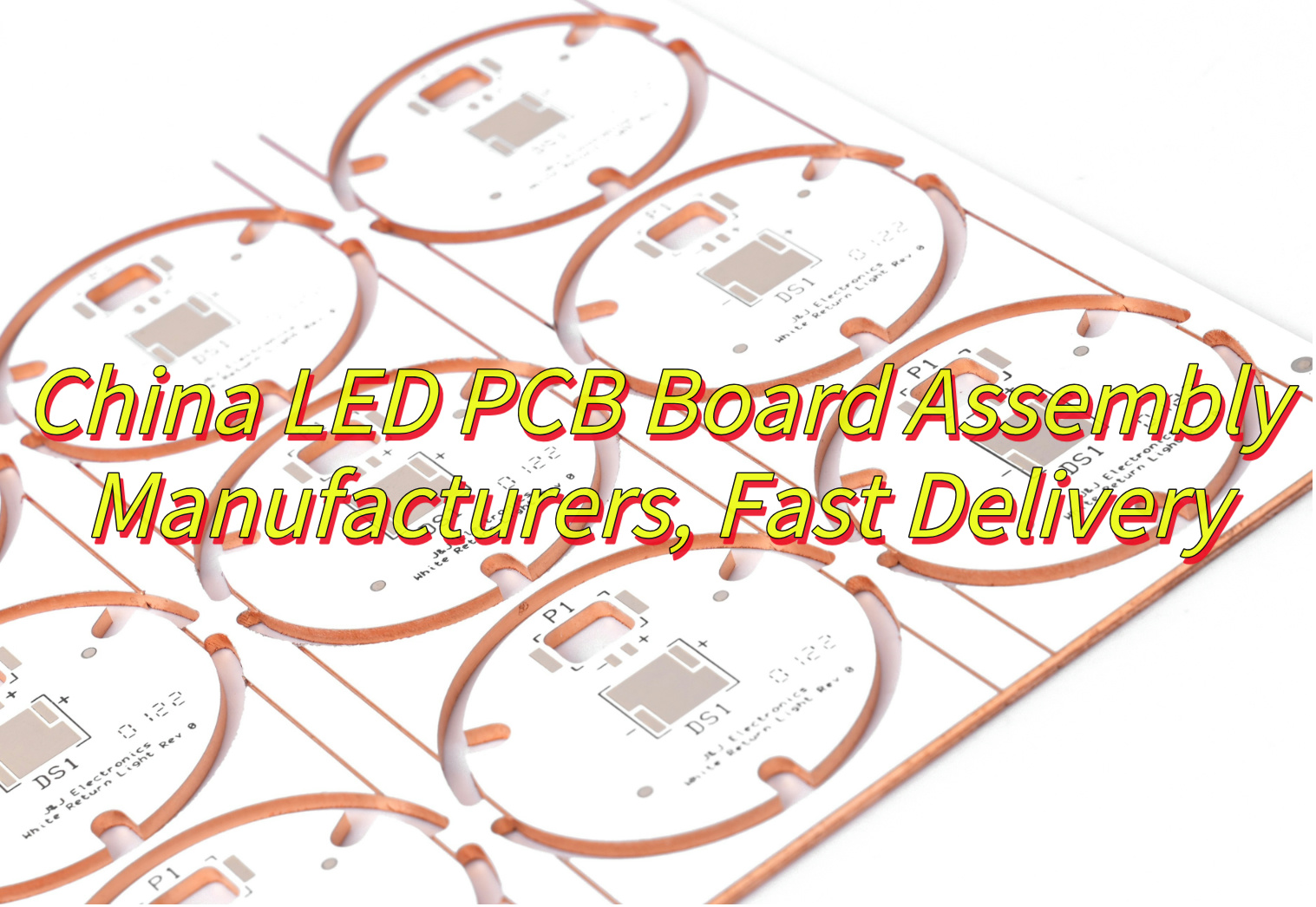
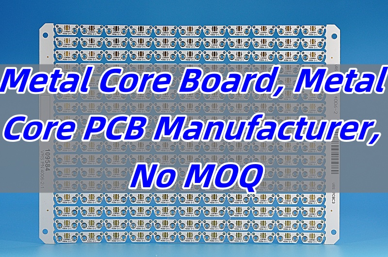
With lightning-fast 24-hour rapid prototyping and production cycles as short as 3–5 days, EBest Circuit (Best Technology) specialize in DIY LED PCB manufacturing with ultra-low MOQs, accepting orders starting at just 1 piece, making us ideal for prototyping or niche projects. Our flexible small-batch customization supports unique board geometries, materials (FR-4, aluminum-core), and finishes, ensuring your idea translates perfectly into functional PCBs. Backed by a dedicated one to one engineering team offering free DFM analysis, we proactively resolve design flaws upfront to avoid costly revisions. Rigorous quality checks using automated optical inspection (AOI) and X-ray testing guarantee flawless LED performance, while competitive pricing—enhanced by shared panelization strategies—keeps budgets lean. From concept to delivery, we combine speed, precision, and personalized support to turn your DIY ideas into reality. Start your project risk-free today if you have any request for DIY LED PCB: sales@bestpcbs.com.
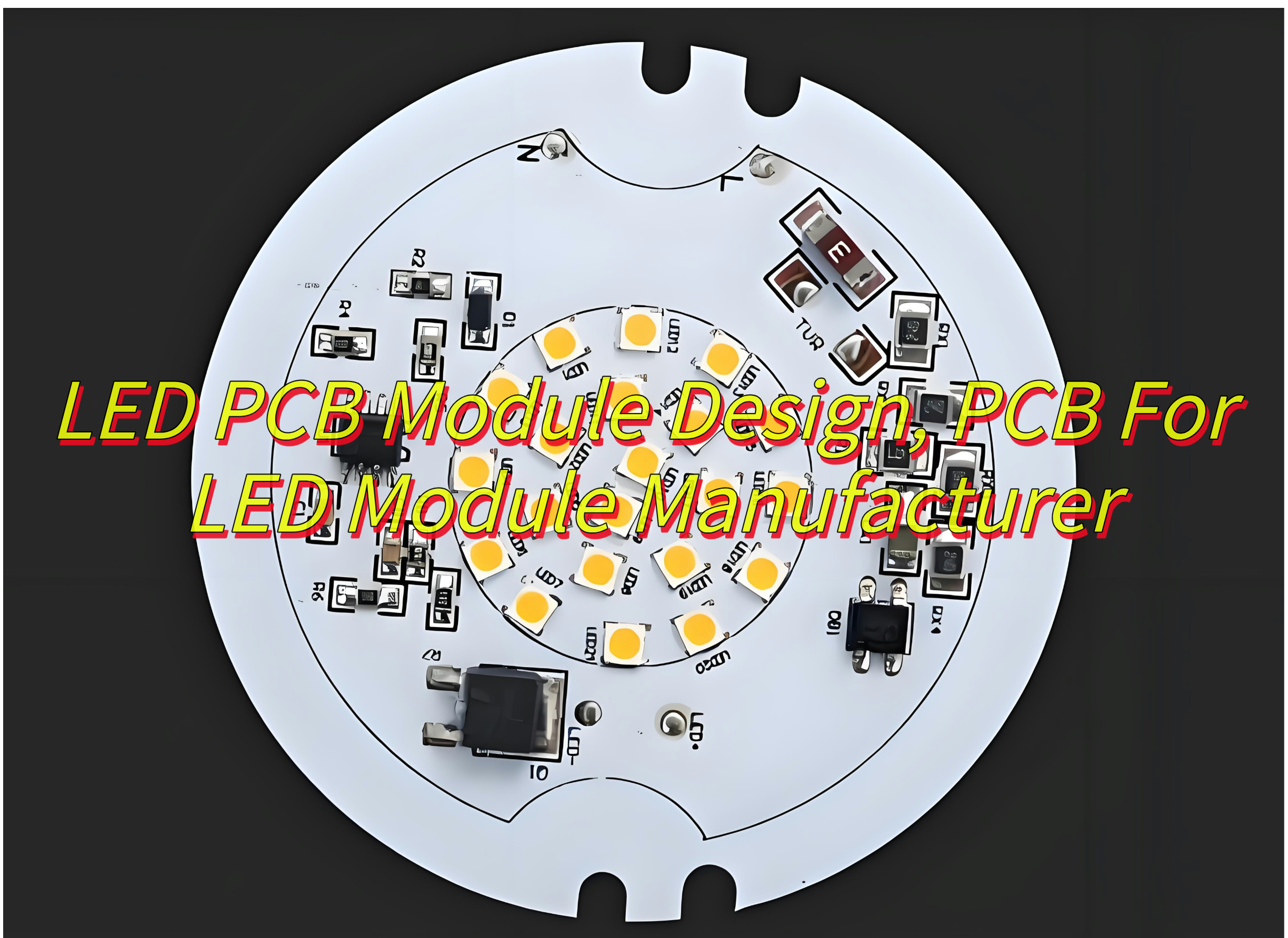
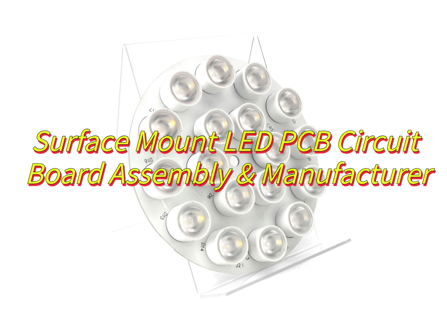
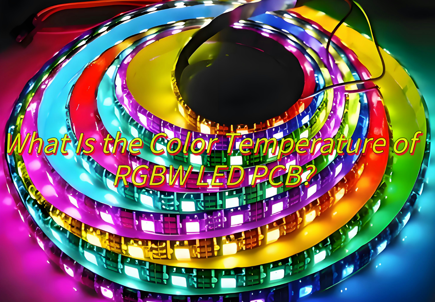
What Is DIY LED PCB?
A DIY LED PCB is a custom-built printed circuit board created by individuals to support and power light-emitting diodes (LEDs) for personalized projects. DIY LED PCB boards are typically designed and assembled by hobbyists or electronics enthusiasts using materials like copper-clad laminate or aluminum substrates, which help manage heat from prolonged LED operation. The process starts with designing a circuit layout using software tools such as KiCad, focusing on trace routing, component placement, and electrical requirements for LEDs. Once the design is finalized, creators transfer it onto a board through methods like toner transfer or chemical etching, followed by soldering components such as surface-mount LEDs or resistors. Common applications include LED ring lights for photography, decorative home lighting, or small-scale electronics like digital clocks. Challenges often involve balancing heat dissipation for high-power LEDs, ensuring stable current flow with correct resistor values, and maintaining soldering precision to avoid short circuits. Unlike premanufactured PCBs, DIY LED PCB version prioritize flexibility in shape, size, and functionality, allowing users to adapt designs for niche purposes like automotive lighting or wearable tech.
What Tools And Materials Are Required For DIY LED PCBs?
Here’s a guideline of tools and materials for DIY LED PCB:
- Soldering Iron and Solder: A temperature-controlled soldering iron ensures precise connections without damaging components. Pair it with lead-free solder for environmental and safety reasons.
- Basic Hand Tools: Needle-nose pliers and wire strippers help manipulate wires and components, while flush cutters trim excess leads neatly.
- Multimeter: This device verifies voltage, continuity, and resistance, acting as your diagnostic tool to troubleshoot faulty connections or short circuits.
- PCB Prototyping Board: Choose a pre-drilled board with copper traces to simplify component placement. Fiberglass boards are durable, while phenolic options are budget-friendly.
- LED Components: Choose surface-mount device (SMD) LEDs for compact designs or through-hole variants for easier soldering. Match their voltage and current ratings to your power supply.
- Resistors and Capacitors: Resistors protect LEDs from current spikes; calculate their values using Ohm’s Law. Capacitors stabilize voltage fluctuations, especially in driver circuits.
- Power Supply: A DC adapter or battery pack should align with your LEDs’ combined voltage and wattage. Include a voltage regulator if working with unstable power sources.
- Thermal Management Materials: Apply thermal paste or pads under heat-sensitive components to prevent overheating. For high-power LEDs, add aluminum heat sinks.
- Connectors and Wires: Use jumper wires or solderable headers for inter-board connections. Stranded wires offer flexibility, while solid-core wires suit permanent setups.
- Safety Gear: Wear eye protection and work in a well-ventilated area. A fume extractor or fan minimizes inhalation of soldering fumes.
- Design Software (Optional): Tools like Eagle or KiCad help plan layouts before soldering, though freehand placement works for simple projects.

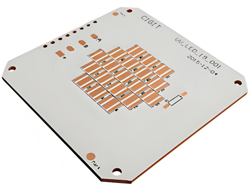
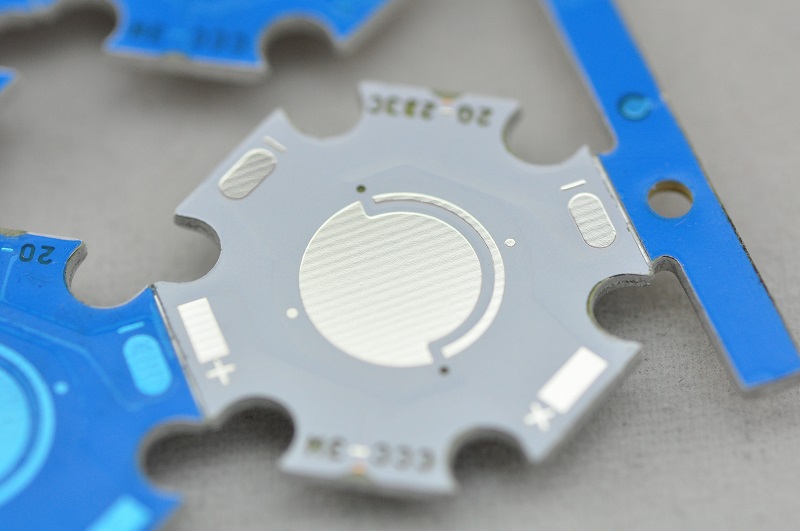
How to Choose the Right Substrate For DIY LED PCB Projects?
Below is how to choose the right substrate for DIY LED PCB projects:
PCB Material Selection:
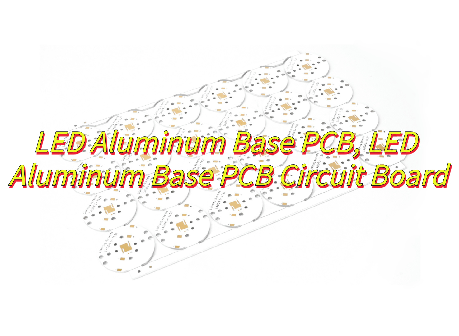
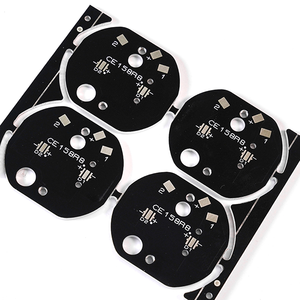
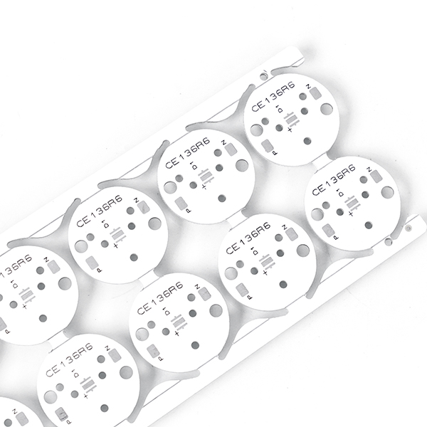
- Choose FR4 glass-reinforced epoxy laminate for its thermal stability and cost efficiency. For high-power LEDs, opt for aluminum-core PCBs to enhance heat dissipation.
LED Placement Strategy:
- Arrange LEDs in linear or radial patterns based on application (e.g., ring lights, panels). Maintain uniform spacing to prevent light intensity variations during transitions.
- Group LEDs with similar color profiles together to simplify current regulation and reduce electromagnetic interference (EMI).
Power Distribution Design:
- Use dedicated traces for each LED color channel (R, G, B) to minimize voltage drops. Ensure trace widths of at least 0.5mm for 1A currents.
- Incorporate decoupling capacitors (100nF ceramic) near LED drivers to filter power supply noise.
Signal Integrity Measures:
- Route data lines (e.g., for WS2812B strips) away from high-current paths. Maintain 90° angles for trace bends to reduce reflections.
- Implement series resistors (22–47Ω) on data lines to match impedance and prevent signal overshoot.
Thermal Management:
- Add thermal vias under LED pads to conduct heat to inner layers. For SMD LEDs, use solder paste stencils to ensure consistent thermal contact.
- Include mounting holes for heat sinks or fans if operating above 70% of LEDs’ maximum rated current.
Microcontroller Placement:
- Position the controller close to LED drivers to shorten data lines. Use a star topology for multi-channel designs to avoid ground loops.
- Add a 10μF electrolytic capacitor across the microcontroller’s power pins to stabilize voltage during PWM bursts.
Testing and Debugging Features:
- Include test points for voltage measurements at critical nodes (e.g., LED cathode, driver VCC).
- Add a 5-pin programming header with VCC, GND, TX/RX, and RESET signals for firmware updates without desoldering.
Layer Stack Considerations:
- For 4-layer boards, allocate Layer 1 for components and signals, Layer 2 for ground, Layer 3 for power, and Layer 4 for auxiliary signals.
- In 2-layer designs, use a solid ground plane and route high-speed signals on the top layer only.
Mechanical Integration:
- Design mounting holes with 0.1mm oversize tolerance to accommodate M2/M3 screws. Add fiducial markers (0.5mm copper pads) for precise assembly alignment.
- Include edge connectors or screw terminals for external power/data inputs.
Prototyping Iterations:
- Start with a perfboard prototype to validate component placement and current requirements. Use a USB power meter to monitor real-time consumption.
- For the first PCB revision, include optional 0Ω resistors to disconnect sections for isolated testing.

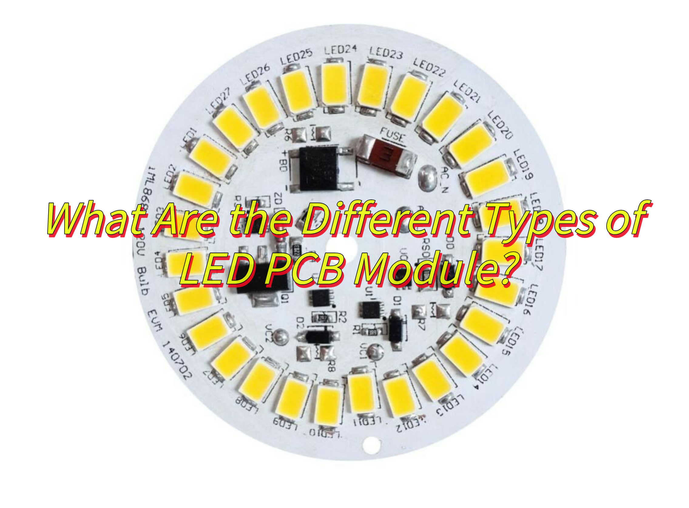
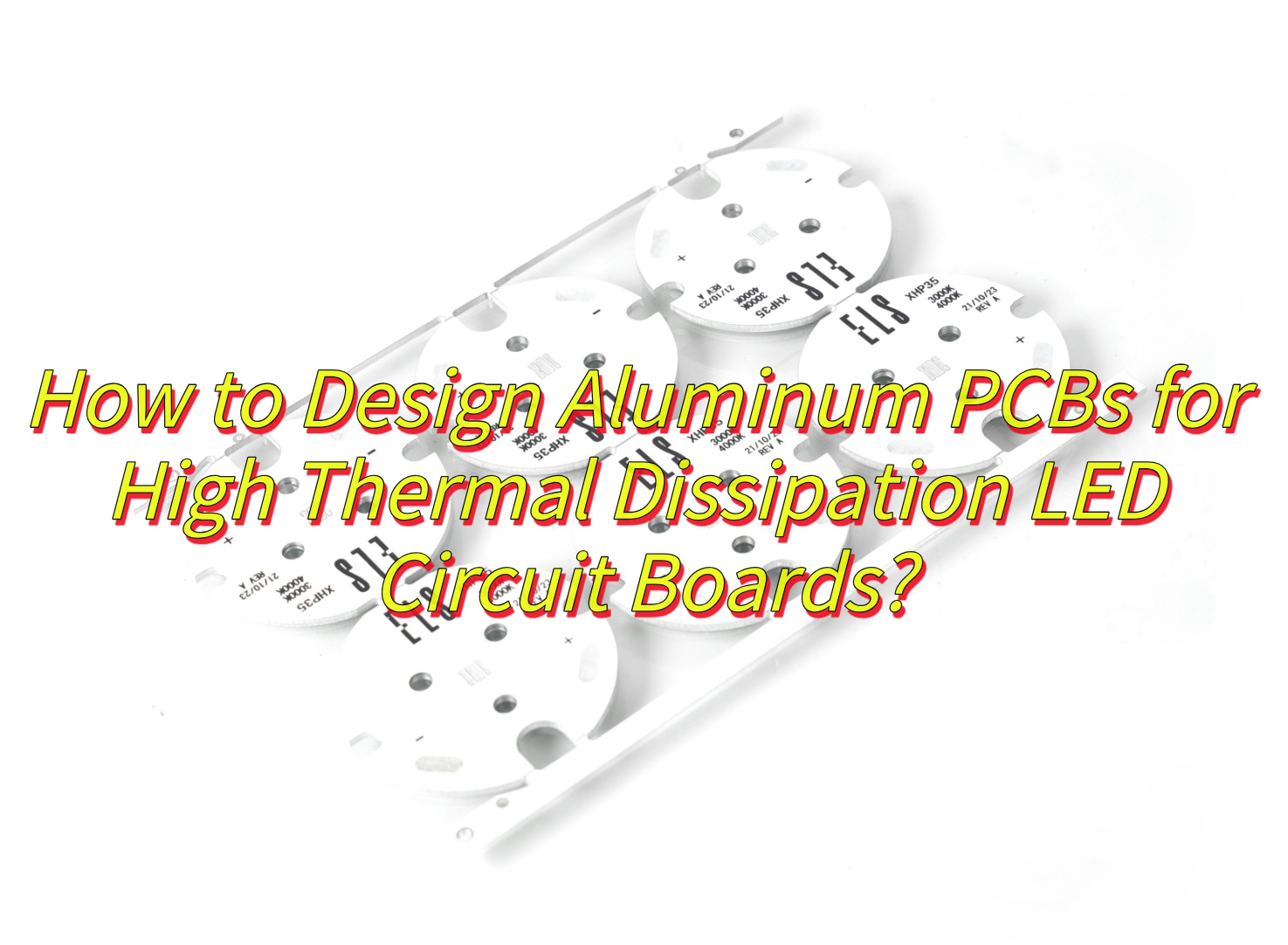
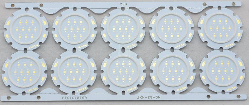
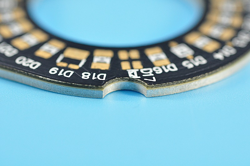
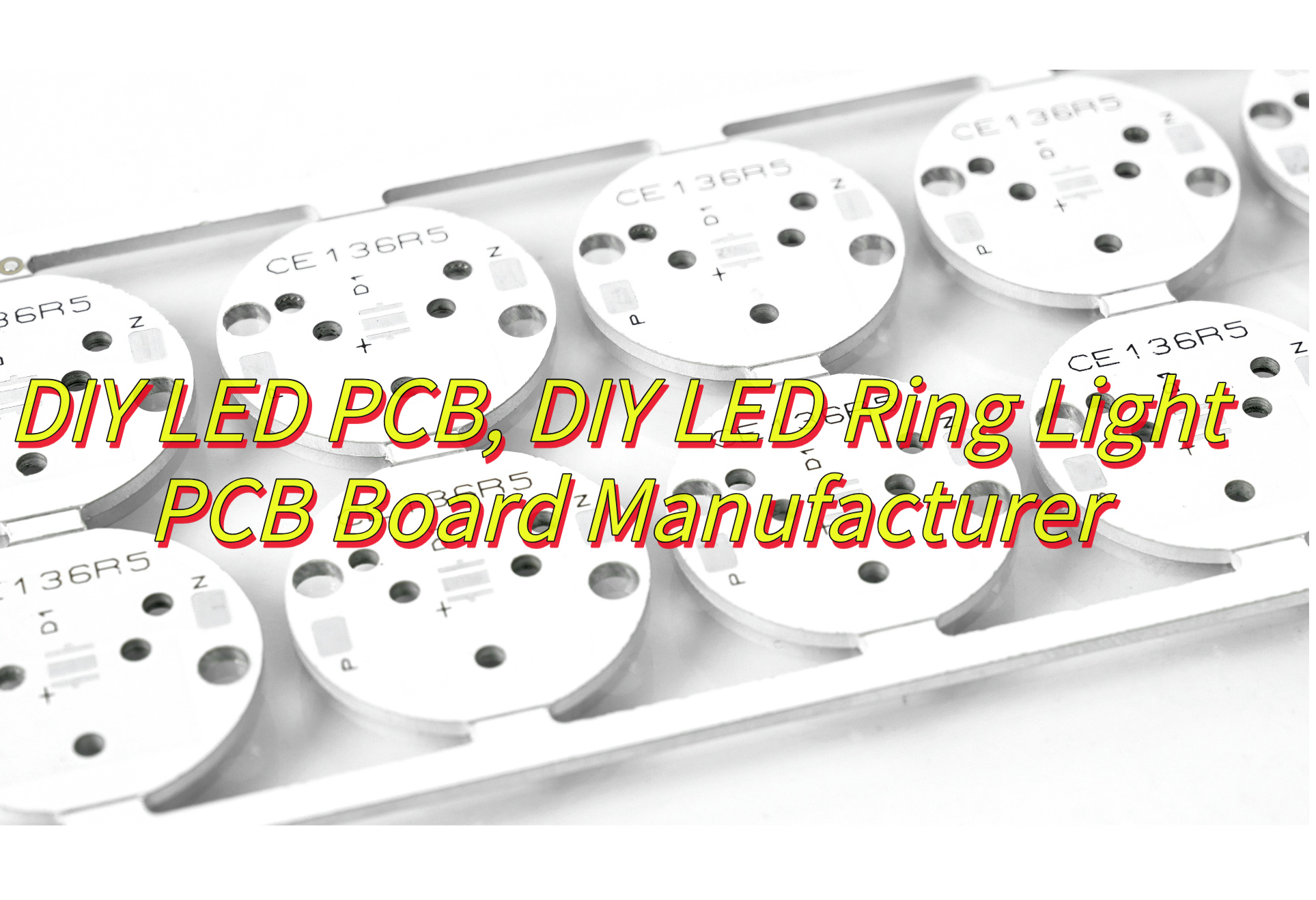
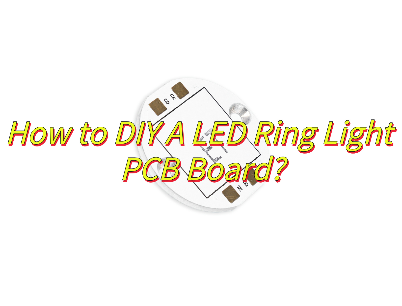
How to DIY A LED Ring Light PCB Board?
This is how to DIY a LED ring light PCB board:
1.Sketch the Circuit Layout
- LED Wiring: Group LEDs into parallel strings (3–6 LEDs per string) to balance current load. Calculate resistors using the formula: resistance equals input voltage minus LED forward voltage, divided by target current. For example, for white LEDs with a three-volt forward voltage and a twenty-milliamp target current, subtract three volts from your input voltage and divide by zero point zero two amps to determine the resistor value.
- Power Path: Add a 1000-microfarad electrolytic capacitor near the power input to smooth voltage spikes. Include a 0.1-microfarad ceramic capacitor by the driver IC to filter high-frequency noise.
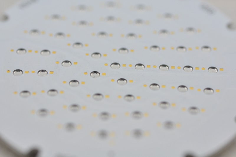
2.Design the PCB Traces
- Route data lines (e.g., for addressable LEDs) away from high-current paths. Use 0.5mm trace widths for signals and 1mm widths for power rails.
- Insert series resistors (22–47 ohms) on data lines to match impedance and reduce signal reflections.
3.Incorporate Thermal Relief Features
- For FR4 boards, add thermal vias (0.3mm diameter, 1mm spacing) under LED pads to conduct heat to inner layers.
- For MCPCB designs, ensure the metal core is exposed on the bottom side for direct contact with heat sinks or metal enclosures.
4.Add Connectors and Controls
- Include a 2.1mm barrel jack for external power and a 5.5mm x 2.1mm DC socket for battery packs. Add a reverse-polarity diode (1N4007) to protect against wiring errors.
- Optional: Integrate a rotary encoder with an LED indicator for dimming control. Use an ATtiny85 microcontroller to generate PWM signals.
5.Fabricate the PCB
- Order a prototype from a manufacturer like JLCPCB, specifying ENIG finish for solderability. Review Gerber files to ensure traces align with your design.
- For DIY fabrication, use the toner transfer method with glossy photo paper. Etch the board using ferric chloride, then drill holes with a 0.8mm carbide bit.
6.Solder Components
- Apply flux to the PCB before soldering to prevent cold joints. Use a hotplate or reflow oven for SMD LEDs to ensure uniform heating.
- Mount the driver IC with thermal paste. Secure heavy components (e.g., electrolytic capacitors) with glue dots to resist vibration.
7.Test and Calibrate
- Measure actual current draw with a USB power meter. Adjust resistors if brightness varies between strings.
- Check light uniformity by photographing the ring through a white diffuser. Identify dark spots using a 1/1000s shutter speed.
8.Assemble the Final Unit
- Attach the PCB to a camera mount using M3 screws and nylon spacers. Add a frosted acrylic diffuser to soften light output.
- Stress-test the board for 2 hours at max brightness. Monitor temperatures with an IR thermometer (aim for <70°C).
9.Iterate and Optimize
- Document thermal performance and power efficiency. Use this data to refine future designs, such as adjusting LED spacing or switching to a hybrid FR4-MCPCB layout.
- Experiment with diffuser materials (e.g., opal acrylic vs. sandblasted glass) to achieve desired light quality.
How to Choose A DIY LED Ring Light PCB Board Manufacturer?
Below are tips about how to choose a DIY LED ring light PCB board manufacturer:
Assess Technical Expertise for Custom Designs
- Verify the manufacturer’s ability to handle precision requirements specific to LED ring lights, such as circular board layouts, fine-pitch soldering for addressable LEDs, and impedance-controlled traces for PWM dimming. Manufacturers with experience in high-density interconnects (HDI) or flexible PCBs are better equipped to manage complex annular designs.
Confirm Rapid Prototyping and Production Cycles
- Prioritize manufacturers offering 24–72-hour turnaround for prototypes and 5–10-day lead times for small batches (10–50 units). Look for facilities with automated assembly lines and real-time order tracking systems to ensure deadlines are met without compromising quality.
Evaluate Flexibility in Small-Batch Orders
- Choose manufacturers specializing in low-minimum-order-quantity (MOQ) production, ideally supporting batches as small as 5–10 boards. This allows iterative testing and design adjustments while minimizing upfront costs. Inquire about mixed-panelization options to reduce waste for multi-design projects.
Review Customization Capabilities
Ensure the manufacturer supports tailored solutions like:
- Custom solder mask colors (e.g., black for reduced light reflection)
- Specialty substrates (aluminum-core PCBs for thermal management)
- Unique finishes (ENIG for solderability, immersion silver for cost efficiency)
Validate Quality Control Processes
- Choose manufacturers with ISO 9001 certification and advanced inspection tools like automated optical inspection (AOI) and X-ray testing. These systems detect soldering defects, trace discontinuities, and alignment errors critical for uniform LED illumination.
Analyze Thermal Management Support
- For high-power ring lights, confirm the manufacturer can integrate thermal vias, copper pours, or metal-core boards to dissipate heat effectively. This prevents LED degradation and ensures stable color output during prolonged use.
Check Responsiveness to Design Feedback
- Partner with manufacturers offering Design for Manufacturability (DFM) feedback within 24 hours. This service identifies issues like insufficient trace spacing or improper pad sizing early, reducing revision cycles and speeding up production.
Compare Cost Structures for Budget Efficiency
- Request itemized quotes highlighting setup fees, material costs, and testing charges. For small batches, prioritize factories with tiered pricing models that scale affordably with order size rather than fixed per-board rates.
How to Reduce Production Cost of DIY LED Ring Light PCB Board?
Here are methods about how to reduce production cost of DIY LED ring light PCB board:
Material Selection
- Choose FR4 substrates over MCPCBs unless thermal demands exceed 1W per LED. Choose 1.0mm thickness instead of 1.6mm to reduce material costs. Use OSP (Organic Solderability Preservatives) surface finish instead of ENIG for non-critical prototype.
Design Simplification
- Reduce LED count by 10–20% through optical simulations (e.g., using DIALux). Replace addressable LEDs (e.g., WS2812B) with parallel strings of static-color LEDs where dynamic effects aren’t required. Simplify traces to 0.3mm width and 0.2mm spacing for cost-effective etching.
Panel Utilization
- Maximize PCB panel space by arranging multiple ring light designs into a single panel. Use v-scoring to separate finished boards, reducing per-unit costs by 15–30%. Confirm with manufacturers if they offer free panelization services for small orders.
Component Standardization
- Use generic 5630/5730 LEDs instead of specialized high-CRI variants for testing phases. Replace precision 0.1% resistors with 1% tolerance types if ±5% brightness variation is acceptable. Source capacitors and diodes from bulk suppliers (e.g., LCSC) to leverage volume discounts.
Manufacturing Partnerships
- Collaborate with manufacturers offering pooled orders, where multiple DIY projects share a production panel. Negotiate price breaks for 50+ unit batches even if your immediate needs are smaller—store excess inventory for future iterations.
Process Optimization
- Avoid plated slots and irregular shapes that require CNC routing. Use 0.8mm drill holes instead of 0.5mm to reduce tooling wear. Choose silkscreen-only labeling instead of gold fingerprints for non-connector edges.
Quality Trade-offs
- Accept 75µm copper thickness instead of 105µm for low-current designs. Use white solder mask instead of black (which adds 10–15% cost) while testing light diffusion effects. Skip impedance control testing for non-critical data lines.
Logistics Strategy
- Combine PCB orders with component shipments to save on freight. Use sea freight for non-urgent bulk orders (4–6 week lead time) instead of air express. Store components in anti-static bags to prevent damage during transit.
Design for Manufacturing (DFM)
- Run DFM checks before submitting files—ensure 0.3mm annular rings, 5mil trace/space, and 0.5mm minimum hole-to-copper clearance. Fixing errors pre-production avoids 50–200 rework fees per batch.
Open-Source Collaboration
- Join DIY electronics communities to share panel space with other makers. Adopt shared designs for non-proprietary features (e.g., power connectors) to split engineering costs.
Can Manufacturers Do Small Quantity Custom DIY LED PCB Board?
Yes, manufacturers can indeed produce small quantity custom DIY LED PCB board. This capability is driven by the growing demand for niche electronics projects, advancements in automated PCB fabrication, and the flexibility of modern production lines. Below is a detailed explanation of how to navigate this process efficiently:
Market Demand and Technological Adaptation
- The rise of DIY electronics and rapid prototyping has pushed manufacturers to accommodate small-batch orders. Modern PCB factories use automated equipment that reduces setup times and costs, making 5–50 unit runs economically viable. For example, some vendors now offer “prototype panels” where multiple small designs are grouped into a single production batch, sharing costs without compromising confidentiality.
Minimizing Order Quantities
- Seek manufacturers with minimum order quantities (MOQs) as low as 5pcs. This is ideal for testing designs before full-scale production. Ask if they waive engineering or setup fees for small orders, as some factories absorb these costs to attract long-term clients.
Accelerating Production Timelines
- Prioritize vendors offering 24–72 hours turnaround for 2-layer boards. Pair this with expedited shipping (e.g., DHL Express) to receive prototypes in 3–5 days. Rapid delivery is critical for iterative design cycles, allowing you to test, refine, and reorder quickly.
Customization Without Compromise
Ensure the manufacturer supports:
- Material Options: FR4, aluminum-core, or flexible substrates (0.6–1.6mm thick).
- Layer Counts: 1–4 layers to balance complexity and cost.
- Surface Finishes: HASL (cost-effective), ENIG (solderable), or immersion silver (premium).
- Advanced Features: Via-in-pad for dense LED arrays, gold fingers for connectors, or impedance control for high-speed signals.
Cost-Saving Strategies
- Panel Utilization: Use free panelization services to fit multiple designs on one panel, reducing per-unit costs by 20–40%.
- Design Simplification: Opt for 0.3mm traces and 0.8mm drill holes to lower etching and drilling expenses.
- Component Sharing: Collaborate with other makers to split panel costs or share non-critical components (e.g., resistors, capacitors).
Quality Assurance Measures
Request details on their inspection protocols:
- Automated Optical Inspection (AOI): Detects solder mask defects and trace issues.
- Electrical Testing: Ensures LED power/data lines are continuous.
- Impedance Testing: For boards using addressable LEDs (e.g., WS2812B).
Design for Manufacturability (DFM)
- Upload Gerber files for a free DFM check before production. Vendors often flag issues like insufficient annular rings or incorrect solder mask colors at no cost, preventing costly reworks.
Logistics and Sourcing Synergy
- Order PCBs and components together to save on freight. Some manufacturers partner with distributors to offer consolidated shipping, reducing customs fees and delivery times.
Community-Driven Collaboration
- Join DIY electronics forums to find makers willing to co-order panels. Splitting a 100-unit panel among 10 projects slashes individual costs while preserving customization.
Responsive Support Networks
- Choose vendors with engineers who answer technical queries (e.g., “Can you route 0.2mm traces for 0603 LEDs?”) within 4–8 business hours. This accelerates troubleshooting during assembly.
How to Solder SMD LEDs on DIY PCB Boards Without Specialized Tools?
Soldering SMD LEDs on DIY PCB boards without specialized tools is achievable with careful preparation and technique. Below are practical steps to ensure reliable connections while minimizing damage to components:
1. Gather Basic Supplies
Start with readily available tools:
- Fine-Tip Soldering Iron (15–30W): Avoid high-power irons to prevent overheating.
- Lead-Free Solder (0.5–0.8mm diameter): Thinner solder flows better on small pads.
- Tweezers (ESD-safe if possible): For holding LEDs during placement.
- Isopropyl Alcohol (90%+): Cleans flux residues post-soldering.
- Magnifying Glass (or smartphone macro lens): For inspecting joints.
2. Prepare the PCB and LEDs
- Clean Pads: Wipe PCB pads with alcohol to remove oxidation or dust.
- Apply Flux: Use a flux pen or liquid flux to improve solder wetting.
- Align Components: Place LEDs using tweezers, aligning the polarity marker (usually a dot or line) with the PCB silkscreen.
3. Tack One Pad First
- Solder One Pad: Apply a small solder blob to one pad using the iron.
- Position LED: Press the LED into the molten solder, ensuring alignment. Allow to cool briefly.
- Reheat and Adjust: If misaligned, reheat the pad and nudge the LED gently with tweezers.
4. Solder the Second Pad
- Feed Solder Carefully: Touch the solder wire to the joint (not the iron tip) while heating the pad. Use just enough solder to cover the pad without creating bridges.
- Avoid Overheating: Limit iron contact to 2–3 seconds per joint to prevent LED damage.
5. Reflow for Better Joints
- Drag Soldering: For dense LED arrays, drag the iron tip across both pads while feeding solder. This ensures even coverage but requires practice.
- Use Solder Wick: If bridges form, clean the tip, place wick over the bridge, and heat until solder flows into the wick.
6. Inspect and Clean
- Check Joints: Joints should be shiny and fillet the pad without protruding beyond the LED edges.
- Remove Flux: Wipe with alcohol-soaked cotton swabs to prevent corrosion.
7. Alternative Methods for Beginners
- Toothpick Method: Dip a wooden toothpick in flux, apply to pads, then touch solder to the toothpick to transfer flux-coated solder.
- Low-Temp Solder Paste: Apply with a toothpick, then heat with a hotplate or iron.
8. Prevent Common Issues
- LED Lifting: Secure components with tape before soldering if tweezers slip.
- Cold Joints: Ensure solder flows smoothly—dull joints indicate poor wetting.
- Thermal Stress: Preheat the PCB with a hairdryer (low setting) to reduce temperature shock.
9. Practice on Scrap Boards
- Test Joints: Solder salvaged LEDs on spare PCB material to refine technique.
- Adjust Iron Tip: File the tip to a chisel shape for better heat transfer.
10. Post-Soldering Checks
- Continuity Test: Use a multimeter to verify no shorts between pads.
- Visual Inspection: Confirm LED polarity under magnification before powering on.
Conclusion
In summary, that’s all about DIY LED PCB’s tools, substrates, ring light design, manufacturer selection, cost-saving strategies, small-batch production, and SMD soldering techniques without special equipment. If you have any issues about DIY LED PCB, welcome to leave a message below this blog.