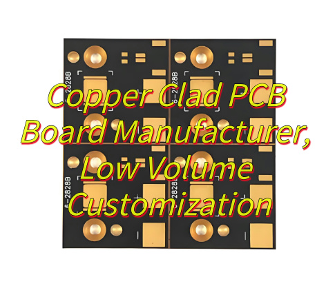
Seeking for copper clad PCB board solution? Discover its material, types, manufacturer selection tips. cost reduction solution, lead time, price affecting factors.
EBest Circuit (Best Technology) solves your copper clad PCB board challenges with unmatched flexibility. We specialize in low-volume customized production with 24-hour rapid turnaround for urgent samples and small batches – no minimum order quantities that stall your R&D. Our transparent pricing policy guarantees no hidden fees, while free DFM analysis identifies cost-saving opportunities before production begins. Our engineering team optimizes panelization designs to maximize material utilization, reducing your PCB costs by up to 30%. With dedicated 24/7 technical support and comprehensive after-sales service, we ensure seamless production from prototype to delivery. Whether you need specialty materials, tight tolerances, or quick-turn fabrication, our copper clad PCB solutions eliminate manufacturing bottlenecks while maintaining quality standards. Welcome to contact us: sales@bestpcbs.com.
What Is A Copper Clad PCB Board?
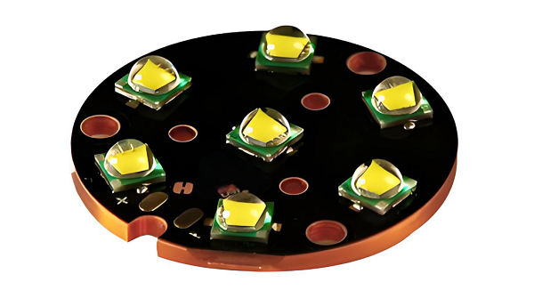
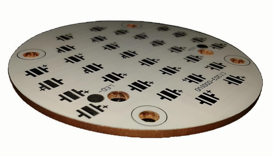
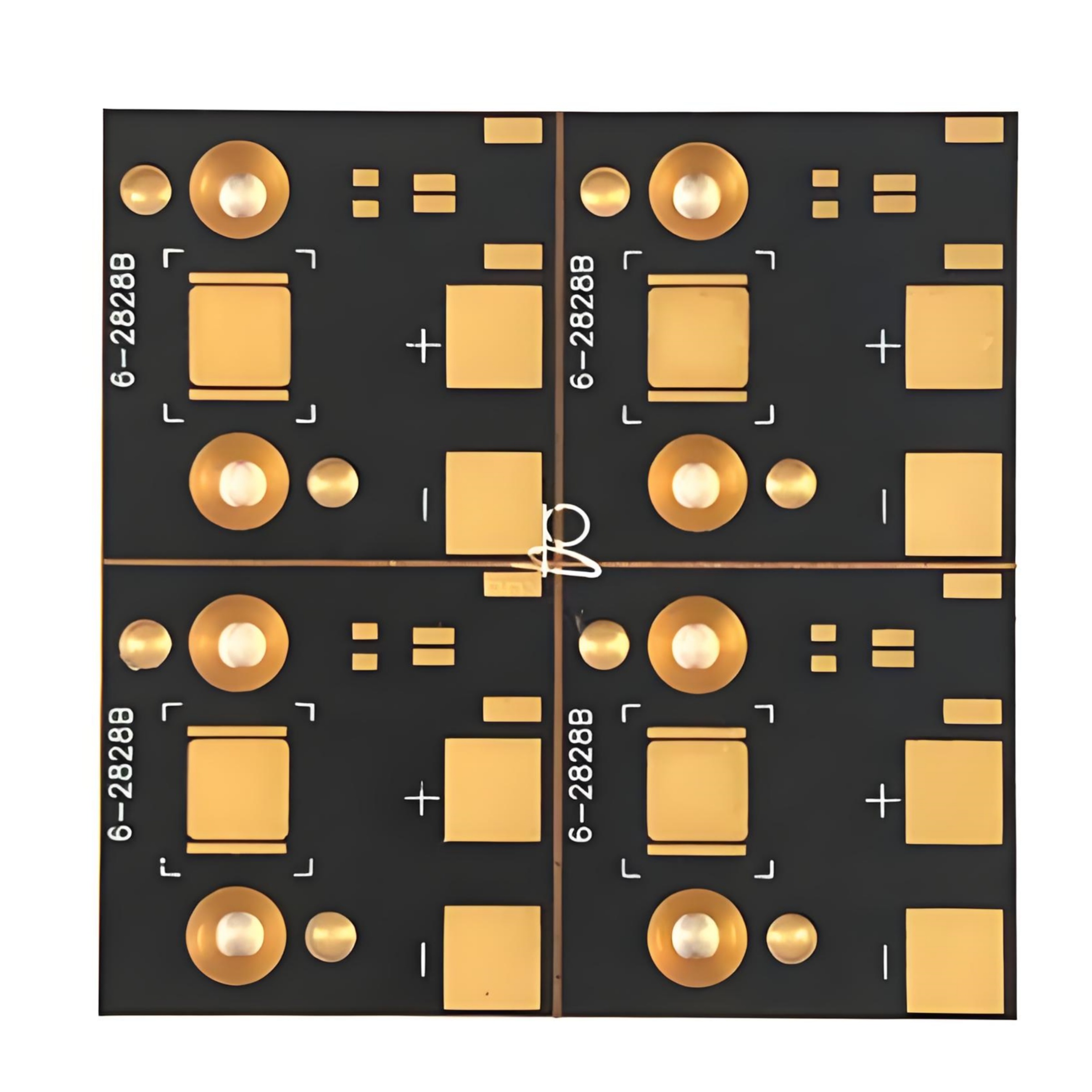
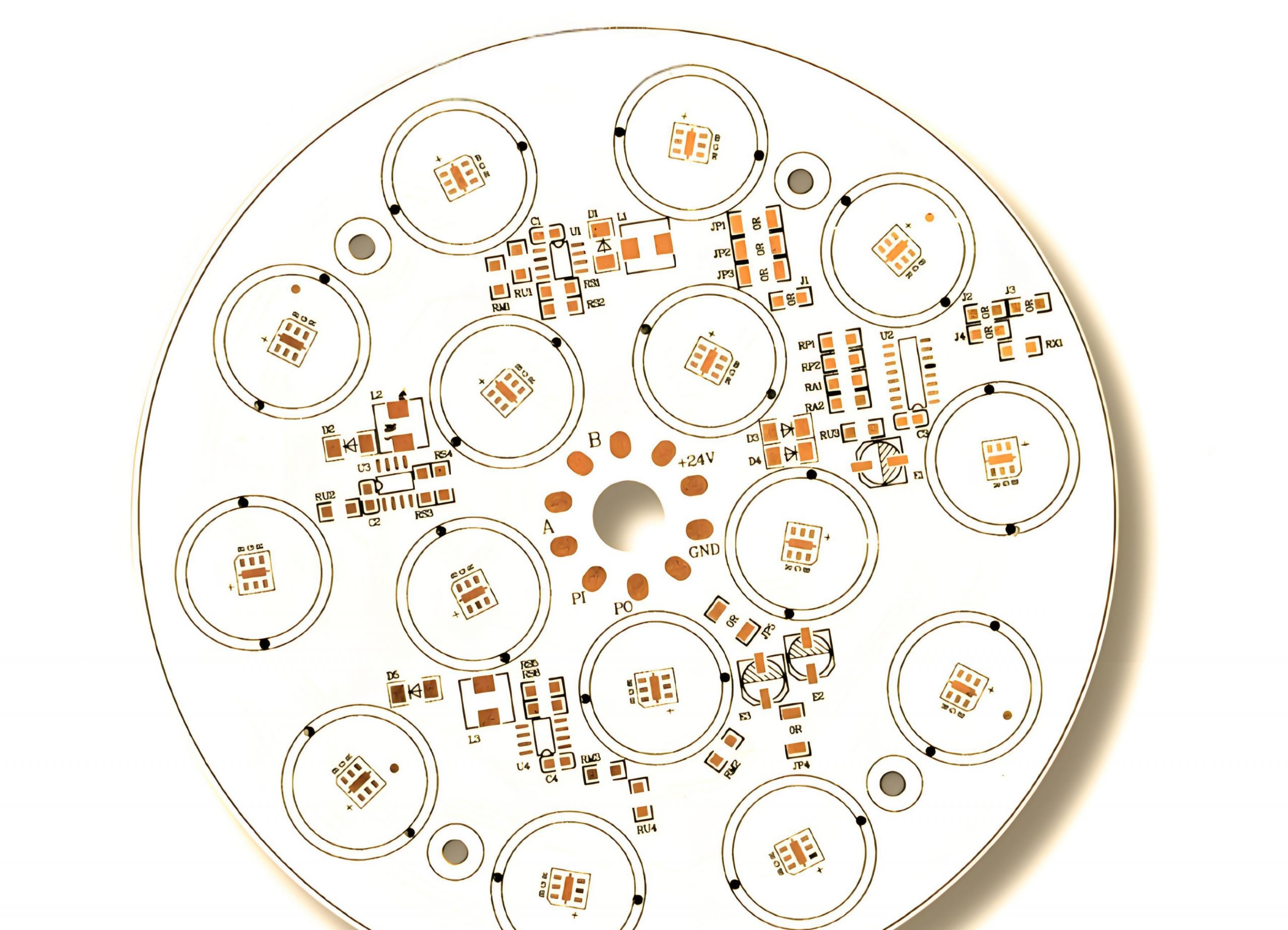
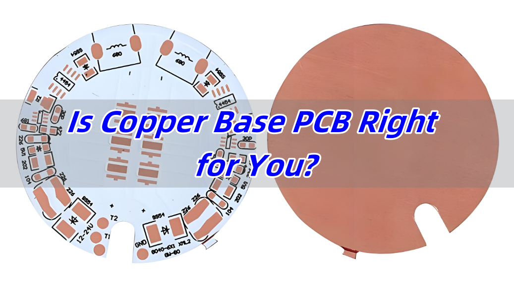
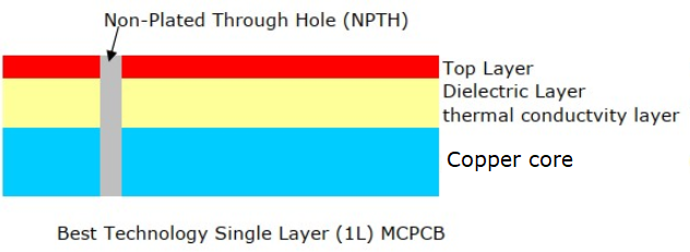
A copper clad PCB board is the fundamental building block of printed circuit boards, consisting of a dielectric substrate laminated with conductive copper foil on one or both sides. The PCB copper clad board serves as the starting material for etching circuit patterns, where unwanted copper is removed to form conductive traces. Copper clad board for PCB applications typically uses FR-4 fiberglass as the base material, though aluminum-backed or flexible versions exist for specialized needs. In manufacturing, copper clad board PCB quality directly impacts signal integrity, with copper purity and thickness being carefully controlled. The copper layer thickness in Copper Clad PCB Board ranges from 1oz to 6oz per square foot depending on current requirements, while the dielectric layer thickness determines impedance characteristics. Advanced PCB copper clad board products may incorporate pre-applied photoresist layers or special surface treatments for high-frequency applications. Proper selection of copper clad board for PCB projects involves balancing electrical performance, thermal management, and mechanical stability requirements. The copper clad board PCB manufacturing process requires precise temperature and pressure control during lamination to prevent delamination issues in final assemblies.
What Is Material of Copper Clad Laminate PCB Printed Circuit Board?
- Conductive Layer: The copper foil in copper clad board for PCB typically comes in 1oz to 6oz thicknesses (35μm to 210μm), with rolled annealed copper being standard for flexible circuits and electrodeposited copper for rigid boards. High-frequency PCB copper clad board versions may use low-profile copper with reduced surface roughness.
- Dielectric Substrate: FR-4 glass epoxy dominates copper clad board PCB applications, combining woven fiberglass cloth with flame-retardant epoxy resin. Alternative substrates include polyimide for flexible Copper Clad PCB Board (up to 260°C tolerance), PTFE for RF/microwave boards, and metal-core (aluminum/copper) for thermal management.
- Adhesive Systems: The bonding between copper and substrate in copper clad board for PCB uses either epoxy-based (standard FR-4), acrylic (flex circuits), or high-temperature polyimide adhesives. Some PCB copper clad board products employ bondply materials with built-in adhesive layers.
- Surface Treatments: Advanced copper clad board PCB materials may feature anti-oxidation coatings (OSP), nickel-phosphorus alloy layers (for ENEPIG), or micro-roughened copper surfaces to improve multilayer lamination reliability in Copper Clad PCB Board stacks.
- Specialty Variants: High-speed digital Copper Clad PCB Board uses low-Dk/Df materials like Megtron 6, while high-power copper clad board for PCB applications employ thick copper (up to 20oz) with ceramic-filled dielectrics. Some PCB copper clad board products integrate embedded passive components.
What Are Types of Copper Clad PCB Board?
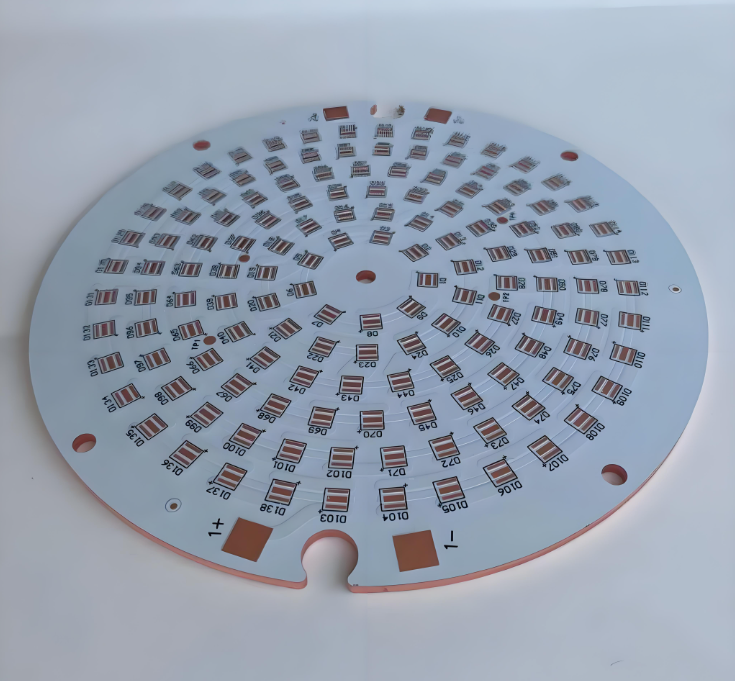
Single-Sided Copper Clad PCB
- Structure: Consists of a single layer of copper foil bonded to one side of an insulating substrate (e.g., FR-4). The non-copper side may include a solder mask or silkscreen.
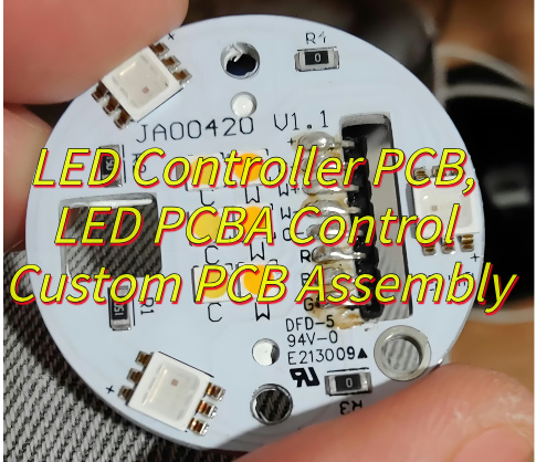
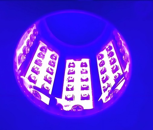
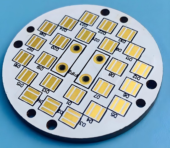
- Applications: Ideal for simple circuits like power supplies, LED lighting, and basic consumer electronics. Common in DIY projects or prototypes.
- Advantages: Cost-effective, easy to manufacture, and suitable for low-density designs.
Double-Sided Copper Clad PCB
- Structure: Features copper layers on both sides of the substrate, connected via plated-through holes (PTHs) or vias.
- Applications: Used in moderately complex circuits such as instrumentation, automotive controls, and industrial equipment.
- Advantages: Enables higher component density and improved signal integrity compared to single-sided boards.
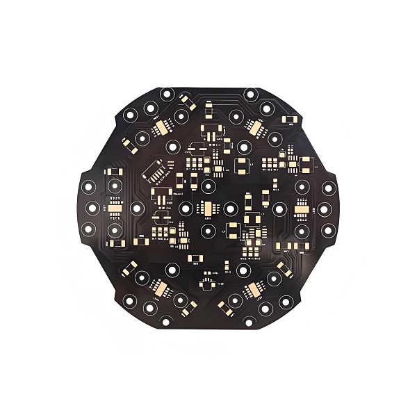
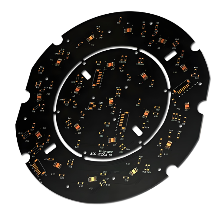
Multilayer Copper Clad PCB
- Structure: Combines three or more conductive layers (copper) separated by insulating prepreg materials. Layers are interconnected via laser-drilled microvias or mechanical drilled vias.
- Applications: Essential for high-speed digital systems, advanced telecommunications, aerospace, and medical devices.
- Advantages: Supports high-density interconnects (HDI), reduces signal loss, and enhances thermal management.
How to Select A Copper Clad PCB Board Manufacturer?
Below are tips about how to select a copper clad PCB board manufacturer:
Verify Export Experience & Compliance
- Prioritize manufacturers with proven export history to your target region (e.g., EU, North America). Request customs clearance documentation (HS codes, certificates of origin) and confirm compliance with local regulations (e.g., REACH, UL, FCC).
- Avoid: Factories lacking experience with import/export paperwork or duty calculations.
Assess Global Logistics Capabilities
- Ensure the manufacturer partners with DHL, FedEx, or freight forwarders for reliable door-to-door delivery. Check if they offer air/sea freight options, customs brokerage, and insurance for high-value shipments.
- Tip: Request lead-time estimates including customs processing (add 3–7 days for international orders).
Review Payment Flexibility & Security
- Choose vendors accepting T/T, L/C, or PayPal for risk mitigation. For first-time orders, Choose 50% deposit + 50% balance against B/L copy.
- Avoid: Upfront full payments or unsecured payment gateways.
Check for Regional Certifications
- For EU markets: Confirm CE marking and RoHS compliance.
- For North America: Require UL 94V-0 and IPC-6012 Class 3 certification.
- For automotive/medical: Validate IATF 16949 or ISO 13485 adherence.
Evaluate Time Zone Collaboration
- Select manufacturers with 24/7 project management or overlapping work hours. For example, a China-based factory pairs well with European clients via late-shift PMs.
- Tool: Use shared project platforms (e.g., Basecamp) for real-time updates.
Audit After-Sales Support for Cross-Border Issues
- Inquire about warranty terms for international shipments (e.g., 12–24 months). Confirm if they handle returns/reworks under Incoterms like DDP or DAP.
- Case Study: A client in Germany once faced a 15% tariff due to incorrect HS coding—ensured the manufacturer absorbed the cost post-dispute.
Leverage Local Representatives or Agents
- For high-stakes orders, partner with a sourcing agent in the manufacturer’s country to conduct factory audits, monitor production, and resolve disputes faster.
- Cost-Benefit: Agents charge 3–5% of order value but save 20–30% in potential rework costs.
How to Cut Copper Clad PCB Board For Reducing Production Cost?
How to Cut Copper Clad PCB Boards to Reduce Production Costs: 7 Practical Strategies
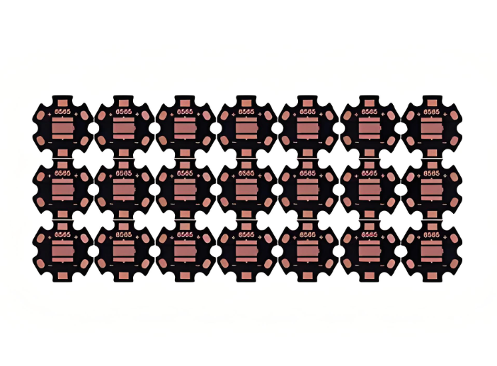
Optimize Panelization Design
- Use nested layouts to maximize material utilization. Simulate cutting paths with software (e.g., CAM350) to minimize scrap between boards.
- Adopt irregular panelization for non-rectangular boards, filling gaps with smaller PCBs or dummy pieces.
Choose Cost-Effective Cutting Methods
- Mechanical Routing: Ideal for prototypes or small batches. Use carbide end mills with programmable depths to reduce tool wear.
- Punching/Die-Cutting: Suitable for mass production of standard shapes (e.g., rectangular boards). Pre-invest in dies for high-volume projects to amortize costs.
- Avoid Laser Cutters unless high precision is mandatory (e.g., <0.1mm kerf), as maintenance and power costs offset savings for most applications.
Implement V-Scoring for Panel Separation
- Use V-shaped grooves (typically 1/3 board thickness) along straight edges to enable easy hand-breaking post-assembly.
- Benefit: Eliminates post-cutting deburring and reduces equipment wear compared to full-depth routing.
Adopt Automated Depaneling Systems
- For high-mix production, deploy pneumatic depaneling routers with automatic tool changers to reduce labor costs.
- For high-volume lines, integrate robotic arms with vision systems to handle fragile boards (e.g., flexible PCBs) without yielding.
Standardize Board Sizes
- Limit custom dimensions to 2–3 standard formats per product line. Reduces setup time and allows bulk purchasing of pre-cut substrates.
- Example: A 500x600mm panel yields 30% more 100x100mm boards than random sizing.
Reduce Edge Margin Allowances
- Trim unnecessary board edges by 1–2mm using precision milling. Maintains functionality while saving material.
- Validate with DFM checks to avoid compromising component placement or test points.
Can Your Manufacturer Accept Low Volume Customization Order?
Yes, EBest Circuit (Best Technology) accept low volume, even 1 pcs customization order.
Flexible Minimum Order Quantities (MOQs)
- Look for factories offering MOQs as low as 1 piece for prototypes or niche applications. Avoid suppliers insisting on 50–100+ panel minimums for custom designs.
- Example: A medical device startup needed 15 units of a 6-layer HDI PCB—a flexible manufacturer adjusted production lines to avoid excess inventory costs.
Rapid Prototyping Capabilities
- Confirm 24–72-hour turnaround for bare boards and 3–5 days for assembled prototypes. Check if they prioritize low-volume orders in scheduling.
- Tool: Request a DFM (Design for Manufacturability) review upfront to resolve issues like trace spacing or impedance mismatches before production.
Material & Process Customization
- Ensure the manufacturer stocks diverse substrates (e.g., FR-4, Rogers, metal-core) and copper weights (0.5oz–6oz) for specialized needs.
- Verify support for controlled impedance, blind/buried vias, and surface finishes (ENIG, immersion silver) at low volumes.
Cost-Efficient Engineering
- Opt for suppliers that waive or reduce NRE (Non-Recurring Engineering) fees for small batches. Some charge flat-rate setup costs instead of percentage-based fees.
- Strategy: Combine multiple low-volume orders into a single production run to split setup costs (e.g., 3 clients sharing a 150-panel batch).
Quality Assurance for Small Lots
- Require 100% electrical testing (flying probe for prototypes) and AOI (Automated Optical Inspection) to avoid defects in low volumes.
- Certification: Check for ISO 9001 or IPC-A-600 compliance, ensuring consistent quality regardless of order size.
Agile Supply Chain Management
- Choose manufacturers with on-demand material sourcing to avoid stockpiling. Some partners align procurement with your forecasts to reduce waste.
- Example: A robotics firm reduced inventory costs by 40% after switching to a supplier offering JIT (Just-in-Time) delivery for low-volume PCBs.
Transparent Pricing Model
- Compare quotes that break down costs by material, fabrication, and testing—not just a per-unit price. Look for discounts on reorders of the same design.
- Tip: Avoid suppliers inflating prices for “customization” if your design uses standard processes (e.g., 2-layer boards with common drill sizes).
How Fast Can Small Be Low Volume Customization Produced?
Simple Designs (2–4 Layers, Standard Materials)
Lead Time: 24–72 hours for bare boards; 5–7 days for assembled prototypes.
Factors:
- Pre-existing material stock: FR-4, 1oz copper, and common solder masks.
- Automated processes: Laser drilling for via formation, automated solder paste stenciling.
- No engineering changes: Finalized Gerber files and BOM.
Example: A 2-layer IoT sensor board with through-hole components can ship in 3 days if materials are in stock.
Moderately Complex Designs (4–6 Layers, Blind/Buried Vias)
Lead Time: 5–10 days for bare boards; 10–14 days for assembly.
Factors:
- Additional fabrication steps: Sequential lamination, controlled impedance testing.
- Material procurement: Specialized substrates (e.g., Rogers 4350B) may require 2–3 days lead time.
- DFM iterations: 1–2 rounds of design feedback to resolve impedance mismatches or drill registration issues.
Advanced Designs (8+ Layers, HDI, Flex-Rigid)
Lead Time: 10–15 days for bare boards; 2–3 weeks for full assembly.
Factors:
- Microvia drilling: Laser or plasma etching adds 3–5 days.
- Lamination cycles: Multiple press operations for rigid-flex sections.
- Testing: Thermal cycling, X-ray inspection for layer alignment.
Emergency/Rush Orders
Lead Time: 24–48 hours for bare boards; 3–5 days for assembly.
Factors:
- Priority scheduling: Overtime shifts or dedicated production lines.
- Premium pricing: 30–50% surcharge for expedited material shipments and labor.
- Limited revisions: No design changes allowed post-confirmation.
Designs Requiring Engineering Verification
- Lead Time: Adds 1–3 days for functional testing (e.g., impedance, power integrity).
- Examples: High-speed digital boards needing TDR (Time-Domain Reflectometry) validation or RF circuits requiring S-parameter analysis.
Post-Production Finishing
- Lead Time: Adds 1–2 days for conformal coating, silkscreen printing, or conformal masking.
- Note: Skipping non-critical finishes (e.g., edge plating for non-connector boards) can save time.
Logistics & Shipping
- Lead Time: 2–5 days (domestic); 5–10 days (international).
- Optimization: Use express couriers (DHL, FedEx) with real-time tracking. Avoid consolidation delays by requesting standalone shipments.
What Factors Affect the Price of Copper Clad PCB Boards?
Here are factors affect the price of copper clad PCB boards:
Material Selection
- Substrate Type: High-frequency materials (e.g., PTFE, Rogers 4000 series) cost 3–5x more than standard FR-4. Metal-core boards (aluminum/copper) for thermal management add 20–40% premium.
- Copper Thickness: Thicker copper (2oz+ vs. standard 1oz) increases etching complexity and material waste.
Layer Count & Stack-Up Complexity
- Multilayer Boards: Each additional layer raises costs by 15–25% due to lamination cycles, prepreg materials, and impedance control requirements.
- HDI (High-Density Interconnect): Laser-drilled microvias (<0.1mm) and sequential build-up processes add 30–50% to per-unit prices.
Order Volume & Economy of Scale
- Small Batches (1–50 pcs): Prices are 300–500% higher per unit due to fixed setup costs (e.g., tooling, DFM reviews).
- Large Runs (10,000+ pcs): Bulk material discounts and streamlined processes reduce costs by 40–60% vs. prototypes.
Surface Finish & Coating
- Premium Finishes: ENIG (Electroless Nickel Immersion Gold) costs 20–30% more than HASL (Hot Air Solder Leveling). Immersion silver or tin adds 10–15%.
- Specialty Coatings: Conformal coatings (acrylic, urethane) or peelable masks for assembly add 5–10% per layer.
Tolerance & Specification Requirements
- Tight Tolerances: Line/space widths <75µm or laser-cut stencils increase costs by 15–20%.
- Controlled Impedance: Requires dielectric constant testing and iterative tuning, adding 10–15% to quotes.
Lead Time & Urgency Fees
- Rush Orders: Expedited production (24–48 hours) incurs 30–50% surcharges for overtime labor and priority scheduling.
- Air Freight: Shipping costs for urgent deliveries can double the total expense for international orders.
Certification & Compliance
- Industry Standards: UL 94V-0 flammability ratings or ISO 13485 (medical) certifications require audits and documentation, adding 5–10% to costs.
- Conflict-Free Minerals: Compliance with Dodd-Frank Act §1502 increases sourcing expenses for tin/tantalum.
Secondary Operations
- Post-Fabrication Steps: Soldermask color matching, gold fingers, or beveled edges add 5–8% per feature.
- Assembly Services: SMT (Surface Mount Technology) or through-hole assembly increases costs by 20–40% depending on component density.
By understanding these factors, you can balance performance needs with budget constraints, optimizing PCB sourcing strategies for both low-volume prototypes and mass production.