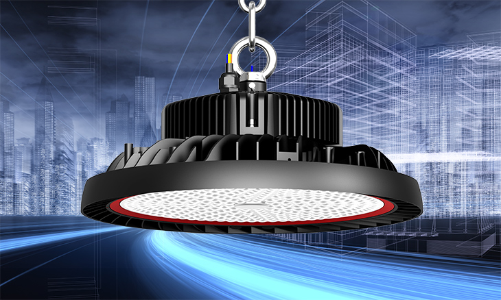
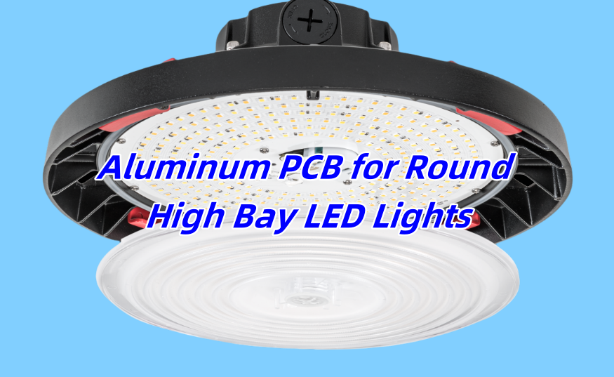
What Is a Round High Bay LED Light?
A round high bay LED light is a type of industrial lighting fixture used in buildings with high ceilings—usually more than 20 feet. These lights are designed in a circular or UFO-style shape to evenly distribute light over large areas. You’ll often find them in warehouses, gymnasiums, factories, airports, and retail stores. Compared to older metal halide or fluorescent systems, round high bay LED lights are more energy-efficient, last longer, and require less maintenance.
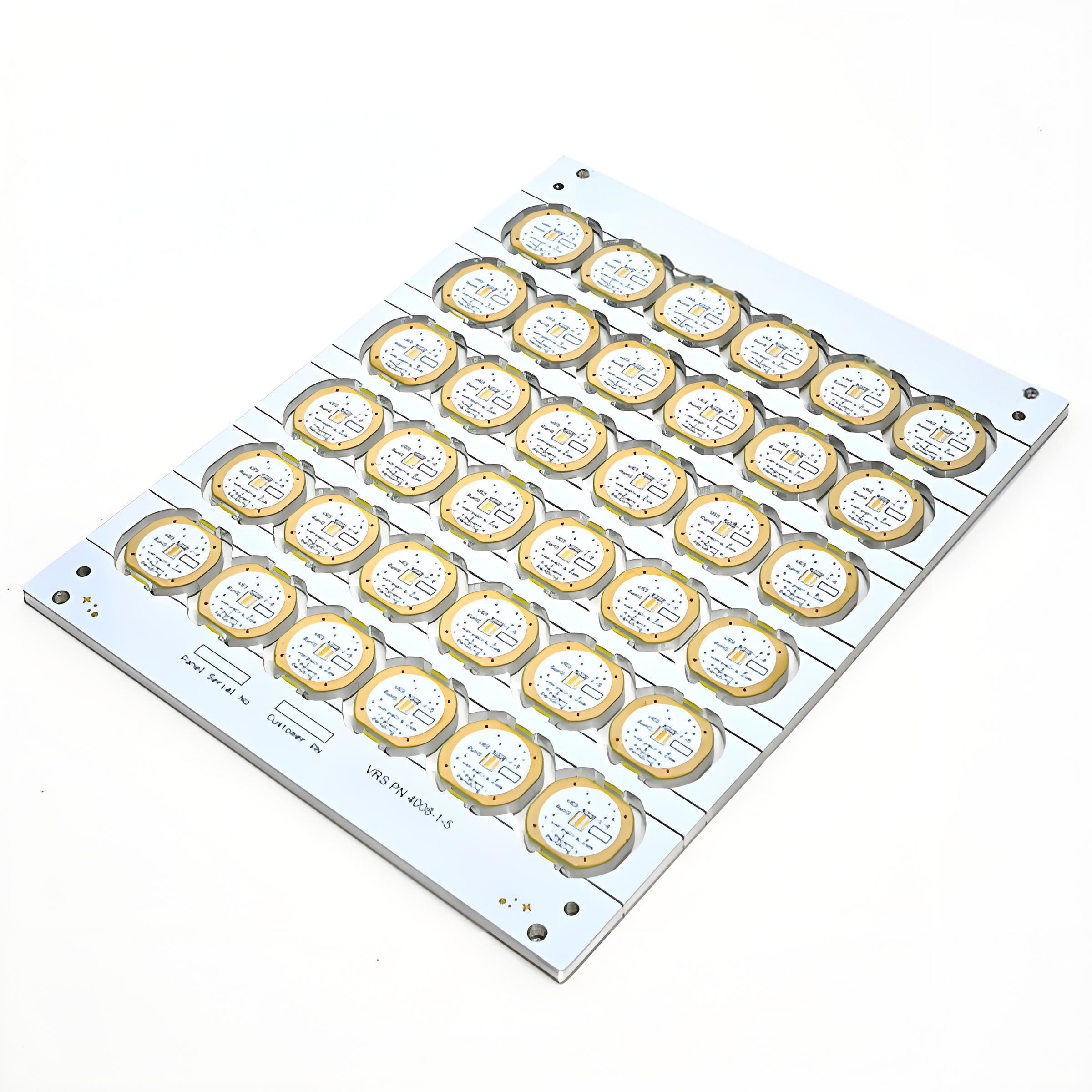
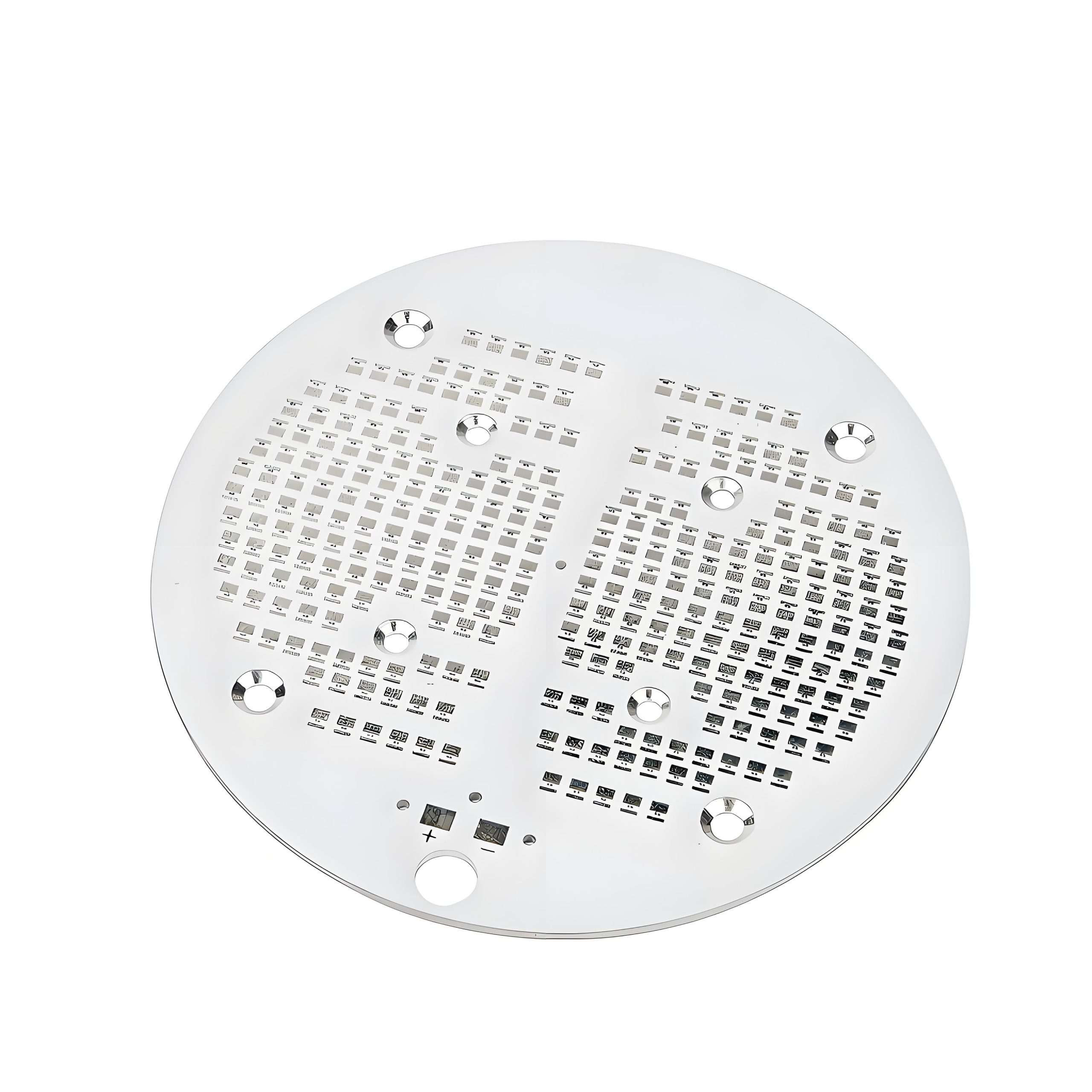
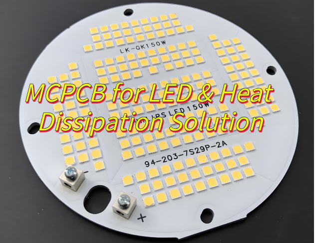
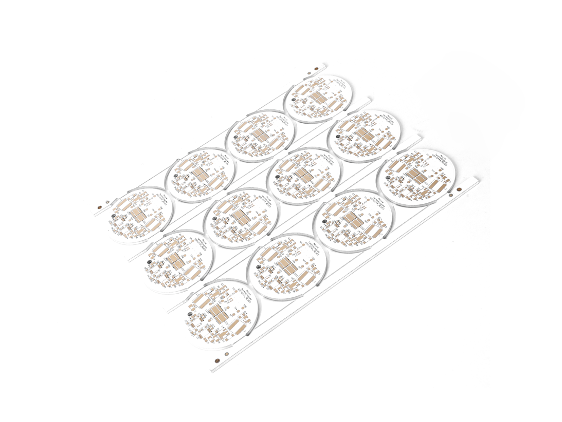
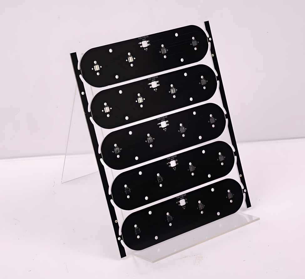
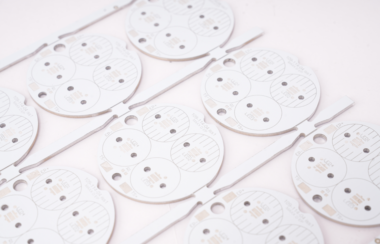
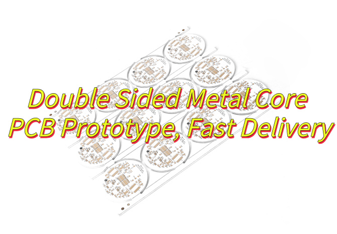
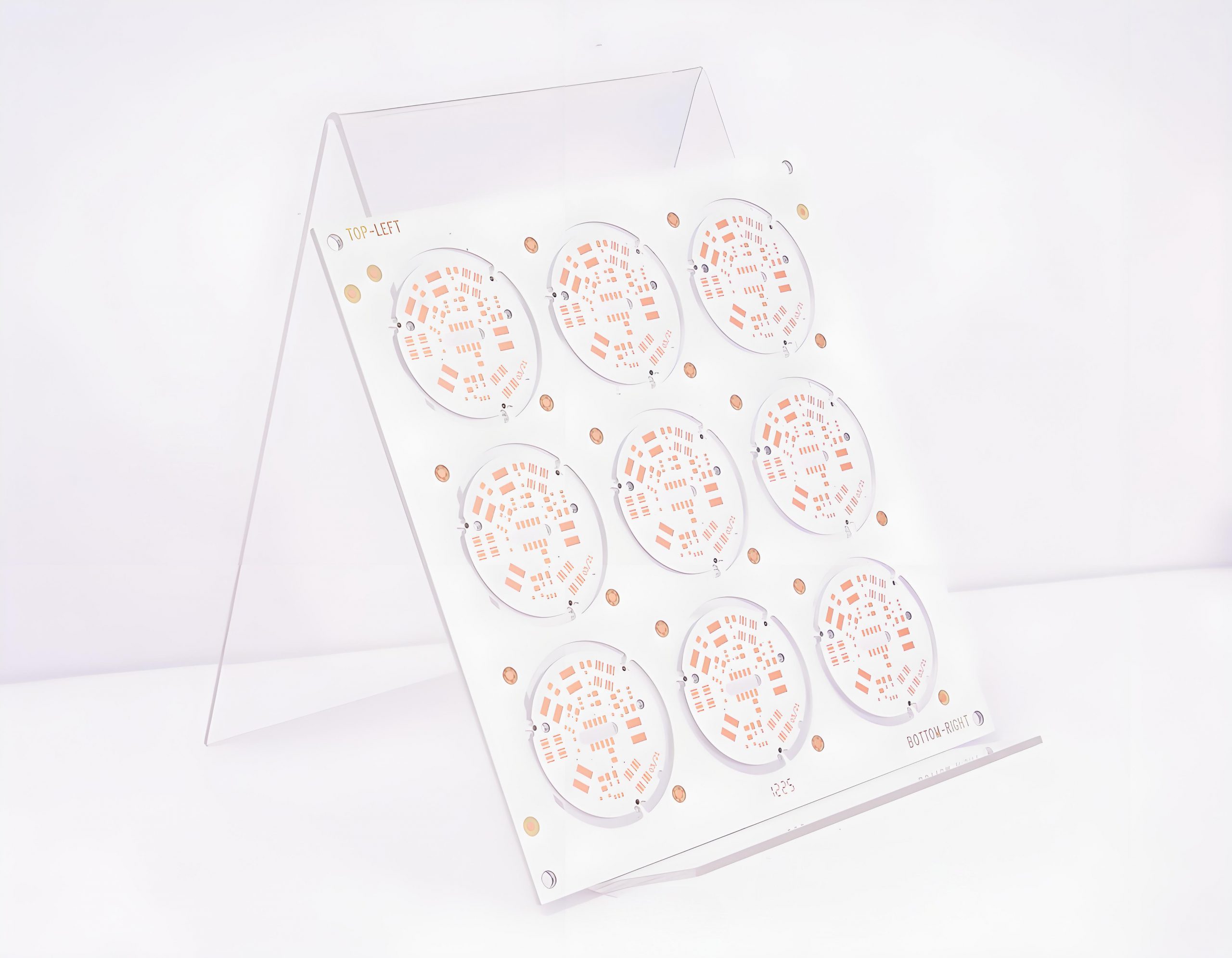
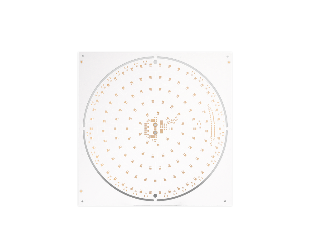
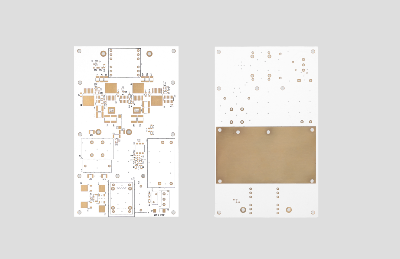
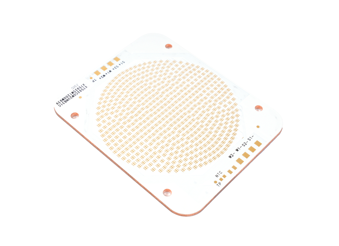
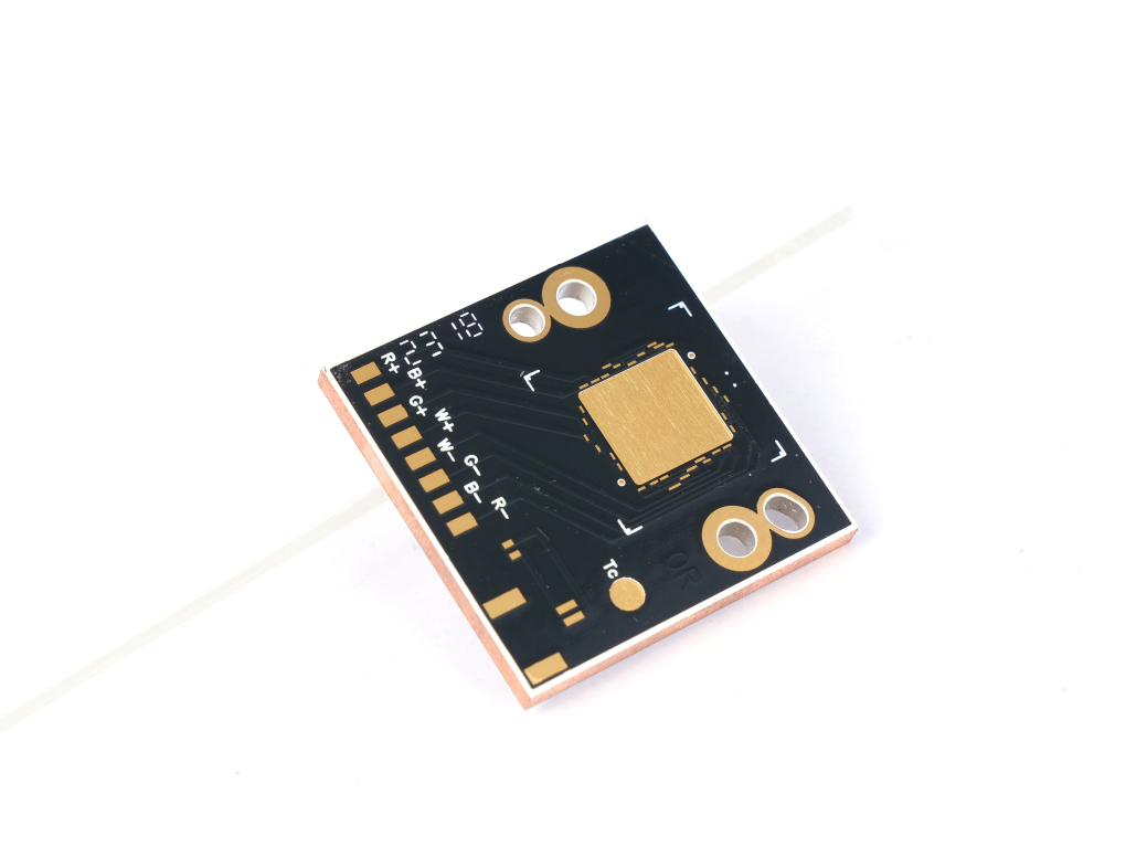
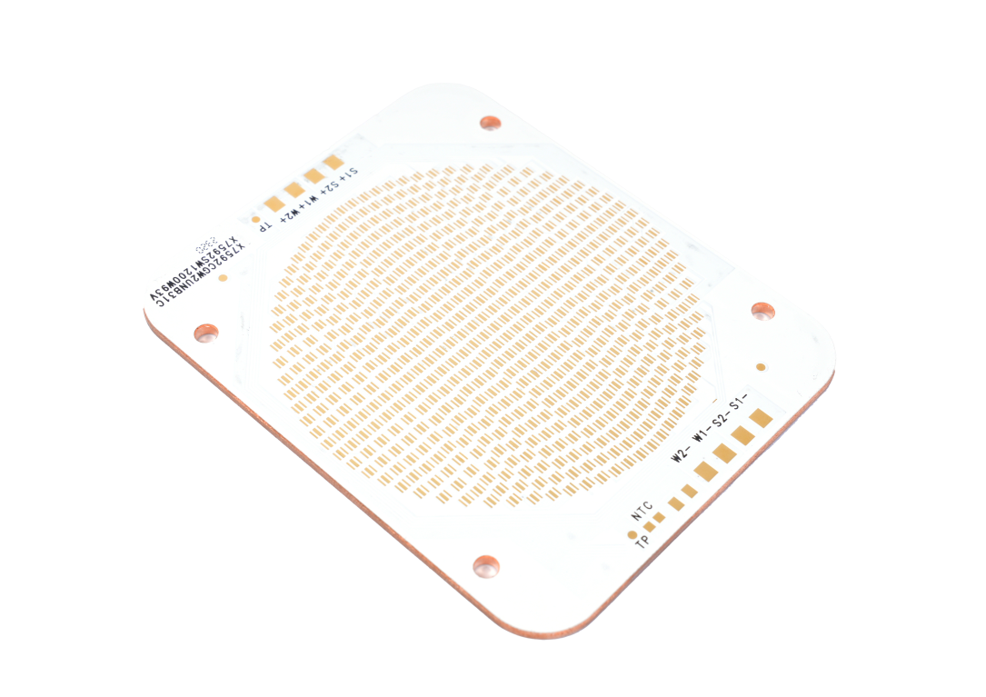
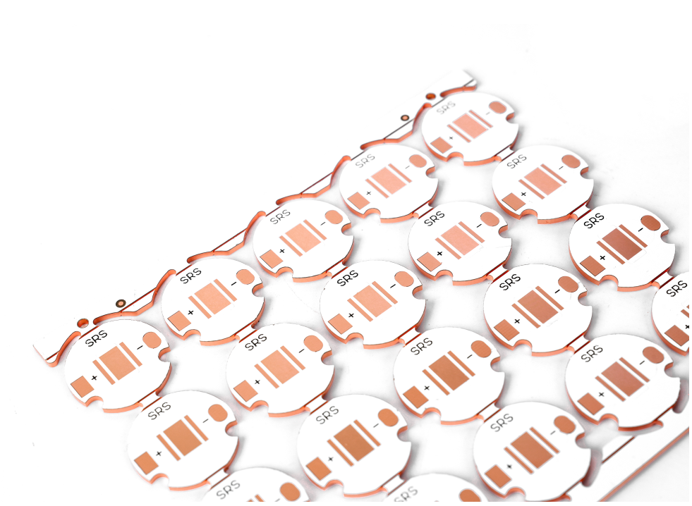
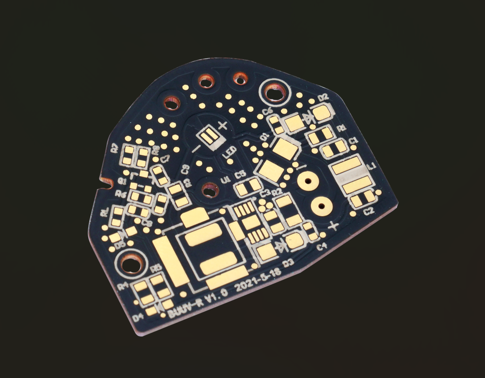
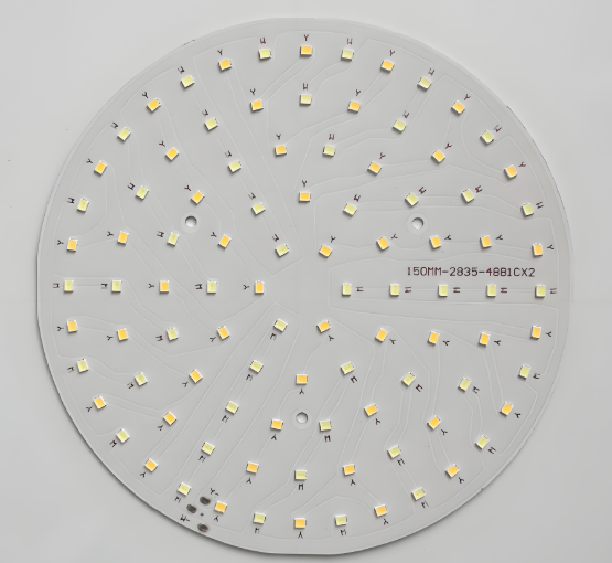
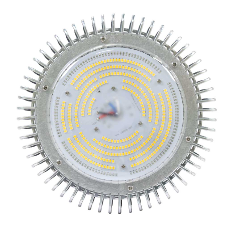
Each fixture typically contains multiple high-power LEDs mounted on a metal-core PCB, surrounded by a reflector and protected by a lens. These components are arranged to direct intense, bright light downward to cover a wide area. The circular layout is easy to install, especially for ceilings where centralized lighting is needed.
Do High Bay LED Lights Get Hot?
Yes, high bay LED lights can get hot—especially after extended use. Although LEDs are more efficient than traditional lighting sources, they still generate heat during operation. The more powerful the light (for example, 100W, 150W, or 200W round high bay fixtures), the more heat it produces.
Unlike incandescent or halogen lights, LEDs don’t emit heat through infrared radiation. Instead, their heat builds up internally around the chip and must be conducted away through the PCB and heat sink. If the heat isn’t managed properly, it can reduce the light’s efficiency, shorten the LED’s lifespan, and even cause failure. That’s why thermal management is crucial for high bay LED lights—and why aluminum PCBs are widely used in their construction.
Why Use Aluminum PCB for High Bay LED Lights?
Aluminum PCBs are preferred in round high bay LED lights because they offer excellent thermal conductivity. In high bay environments, LED chips are packed closely together on a board, creating a concentrated source of heat. Aluminum PCBs help move this heat away from the chip quickly, reducing the risk of overheating.
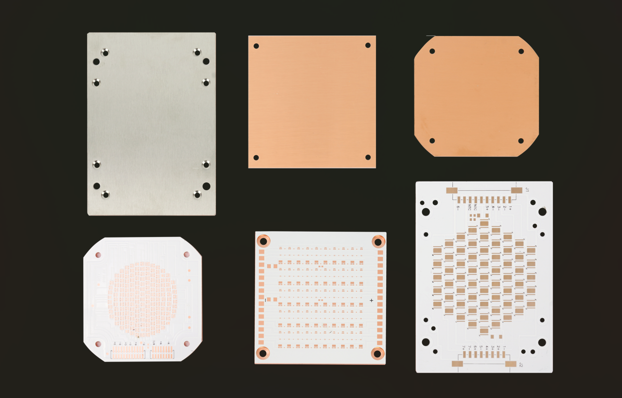
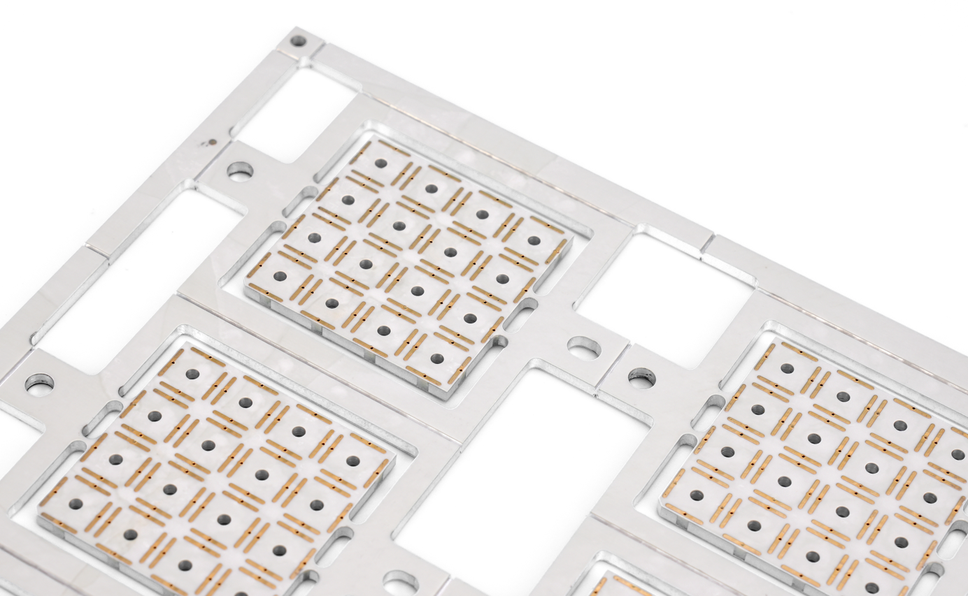
Traditional fiberglass PCBs (like FR4) are not good at handling thermal loads. They trap heat near the components, which can lead to LED failure. In contrast, aluminum PCBs consist of a metal base layer, a dielectric insulation layer, and a copper circuit layer.
Using aluminum PCBs in high bay LED lights also helps to maintain consistent brightness, reduce light degradation over time, and support longer operating lifespans—often 50,000 hours or more.
Advantages of Using Aluminum PCB
1. Aluminum PCBs rapidly transfer heat away from LED chips, so that they can reduce the temperature at the LED junction and maintains stable light output over time.
2. High bay lights are often used in demanding environments like factories and warehouses. The base material of aluminum PCB is metal, so they can provide better structural stability and resistance to vibration and moisture.
3. When LEDs operate at lower temperatures, their lumen output remains consistent for years with minimal degradation.
4. Despite their strength, aluminum PCBs are relatively lightweight compared with copper core PCB. This can reduce the overall weight of the high bay fixture, make it easier to install and handle.
5. Though aluminum PCBs cost more than standard FR4 boards, their durability, reliability, and low maintenance result in long-term savings—especially in industrial settings where lighting failures can be costly.
1W vs 2W vs 3W Aluminum PCB: Which One Is Best?
In aluminum PCBs used for round high bay LED lights, the terms 1W, 2W, and 3W refer to the thermal conductivity of the dielectric layer between the copper circuit and the aluminum base, not the power of the LEDs themselves.
It’s measured in watts per meter-kelvin (W/m·K) and indicates how efficiently heat is transferred from the copper to the aluminum core. The main job of dielectric layer is to insulate electrically while conducting heat away from the LED components. Here’s how they compare:
- 1W Aluminum PCB
1W PCBs are used for low-power applications where heat is minimal. They’re suitable for small or decorative lights but not recommended for industrial high bay systems. The heat dissipation capacity is limited, and using them in high-power lights may cause overheating.
- 2W Aluminum PCB
2W PCBs offer better heat conductivity than 1W versions and are often used in mid-power LED lights, such as 50W to 100W systems. They provide a balance between performance and cost, and they work well in moderately demanding environments.
- 3W Aluminum PCB
3W PCBs are designed for high-performance LED lighting. They are ideal for 150W to 200W round high bay fixtures, where multiple high-output LEDs are densely packed. These boards handle more heat and offer higher durability under continuous operation.
So, which one is best? For round high bay LED lights used in industrial or commercial buildings, 3W aluminum PCBs are usually the best option. They support powerful LEDs, provide excellent thermal control, and reduce the risk of system failure.
Round High Bay LED Lights PCB Design Guide
Designing a printed circuit board (PCB) for round high bay LED lights requires special attention to thermal management, electrical performance, mechanical stability, and spatial efficiency. These lights operate in high-ceiling environments and typically involve high power, which means the PCB must handle significant heat while maintaining long-term reliability.
1. Shape and Form Factor
Since the fixture is round, the PCB is typically designed in a circular shape to match the housing and ensure symmetrical light distribution. This helps maintain uniform brightness across the target area and improves heat spreading across the surface.
To design the board:
- Use radial symmetry when placing LED chips to maintain uniform light output.
- Create concentric LED rings to balance thermal and optical performance.
- Align mounting holes and cutouts with the housing’s mechanical features for secure fitting.
2. Material Selection: Aluminum Core
The aluminum substrate is the foundation of thermal performance. Choose high-quality aluminum cores with good thermal conductivity—typically in the range of 1.0 W/m·K to 3.0 W/m·K.
Common material stack-up:
- Top layer: Copper circuit (usually 1oz or 2oz)
- Middle layer: Dielectric insulating layer (optimized for thermal transfer, usually 75–150μm thick)
- Bottom layer: Aluminum base (typically 1.0–1.6mm thick)
Noted: The thicker the base, the higher the dielectric layer value, the better the heat transfer, but also the heavier and costlier the board becomes.
3. Copper Thickness and Trace Width
For high-power LEDs, the copper thickness should be:
- 1oz (35μm) minimum for moderate power (≤100W)
- 2oz (70μm) or 3oz (105μm) for high-power designs (≥150W)
Use wide copper traces to reduce resistive losses and avoid overheating. Calculate trace width based on expected current using IPC-2221 standards.
4. Thermal Management Techniques
Heat dissipation is critical in high bay LED lights. Key design methods include:
- Use direct thermal path: Use thermally conductive vias or metal-core structures to transfer heat from LEDs to the aluminum base.
- Thermal vias: For multilayer aluminum PCBs (if needed), add thermal vias below heat-generating components to improve vertical heat flow.
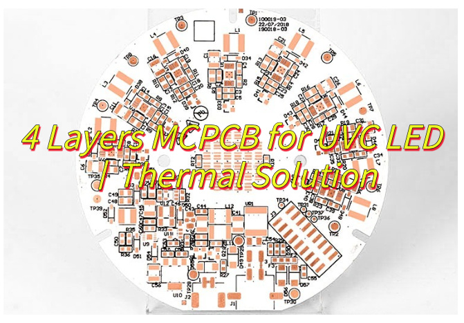
5. LED and Component Placement
Carefully plan the placement of LEDs, drivers, resistors, and protection components:
- LEDs: Distribute evenly in radial or concentric patterns to ensure uniform illumination.
- Driver ICs and capacitors: Place these in cooler areas away from dense LED zones to reduce thermal interaction.
- Thermistors or temperature sensors: Add for real-time temperature monitoring and safety.
Avoid placing heat-sensitive components directly beside high-heat sources.
6. Electrical Isolation and Safety
Since aluminum is conductive, electrical insulation is critical. The dielectric layer between the copper circuit and aluminum base must withstand at least 2–3kV isolation voltage. It is better to consult your PCB manufacturer to get a best solution.
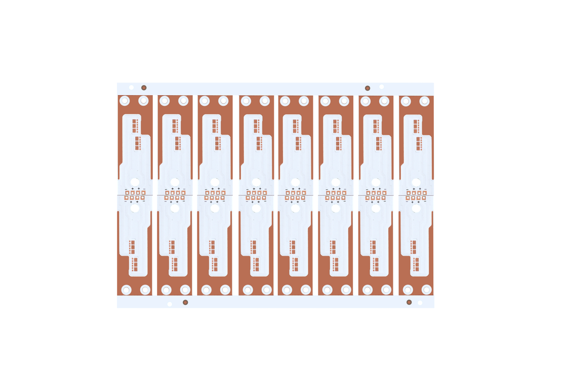
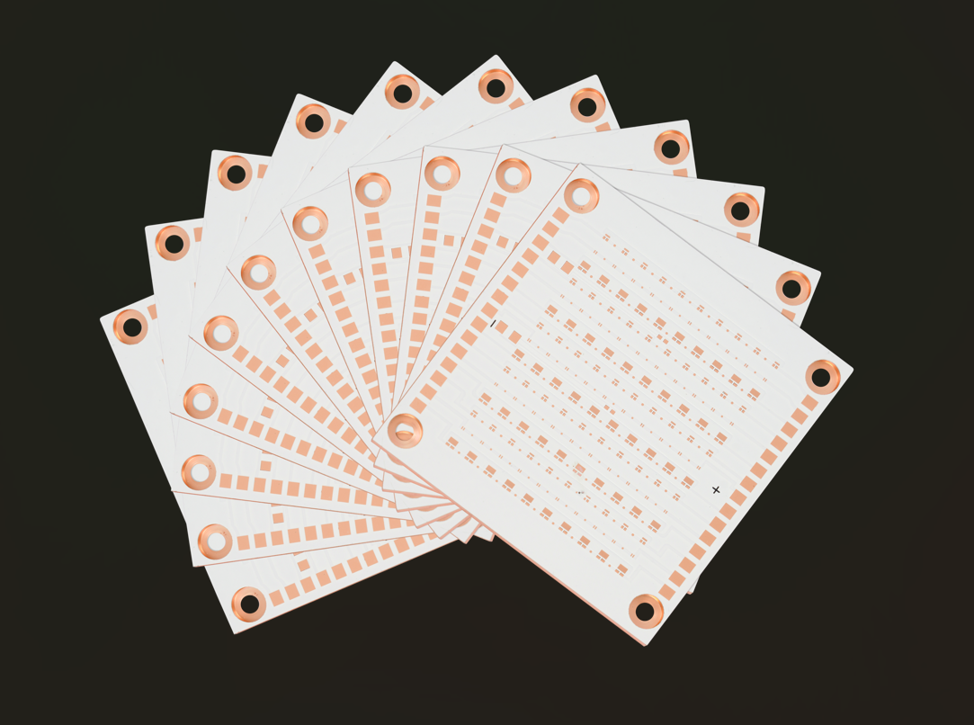
Our Aluminum PCB Manufacturing Capability
| Item | Capabilities |
| Layer Count | 1 – 10 Layers |
| Max Board Dimension | 24” × 64” (610mm × 1625mm) |
| Min Board Thickness | 0.6mm |
| Max Board Thickness | 4.0mm |
| Conductor Thickness | 0.5oz – 10oz |
| Min Line Width/Line Space | 4/4mil (0.10/0.10mm) |
| Min Hole Diameter | 10mil (0.25mm) |
| Min Punch Hole Diameter | 0.12” (3.0mm) |
| Min Hole Spacing | 16mil (0.4mm) |
| Min PAD Ring (Single) | 3mil (0.075mm) |
| PTH Wall Thickness | Normal: 0.59mil (15μm); HDI: 0.48mil (12μm) |
| Min Solder PAD Diameter | 14mil (0.35mm) |
| Min Soldermask Bridge | 8mil (0.20mm) |
| Min BAG PAD Margin | 5mil (0.125mm) |
| PTH/NPTH Dia Tolerance | PTH: ±3mil (0.075mm); NPTH: ±2mil (0.05mm) |
Where Can I Get an Aluminum PCB Quote?
If you’re sourcing aluminum PCBs for round high bay LED lights, it’s important to choose a supplier with experience in LED lighting applications. Getting the right material, thickness, and thermal configuration can make a big difference in your product’s performance.
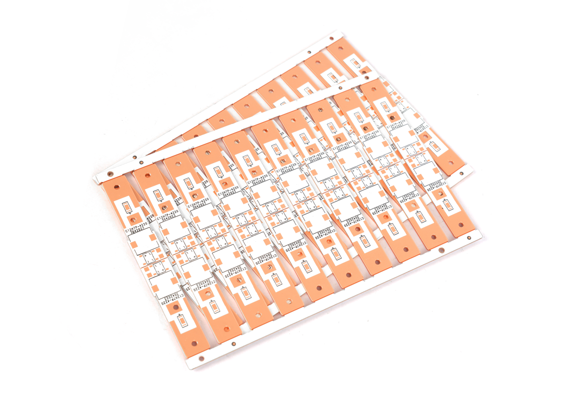
EBest Circuit (Best Technology) is a professional PCB manufacturer offering customized aluminum PCBs for LED lighting. We support a wide range of applications, from low-power LED modules to high-power round high bay LED lights. Our services include:
- Custom shapes PCB designs, like round, rectangle, irregular…
- Various materials available, aluminum, copper, FR4, ceramic and so on
- 3W aluminum PCB production
- Fast prototyping and mass production
- Strict quality control ISO quality control system
- Competitive pricing and fast delivery
- No MOQ & fully flexible
- Turnkey services from PCB design, components sourcing to PCB assembly
- SMT factory both in China & Vietnam
To get a free aluminum PCB quote, simply send us your design files or requirements. Our engineering team will review your project and offer the best solution based on your needs and budget.
If you’re ready to start a new LED lighting project or improve your current product line, partnering with EBest Circuit (Best Technology) can help to save time, reduce costs, and deliver reliable lighting solutions to you.
FAQs
1. What material is used in aluminum PCBs for high bay lights?
Aluminum PCBs use a base of aluminum metal, a dielectric layer for insulation, and a copper layer for circuit routing. This stack helps transfer heat from the LEDs to the fixture housing efficiently.
2. Can I use FR4 PCB in round high bay LED lights?
FR4 can be used for very low-power LEDs, but it’s not suitable for high bay lights due to poor heat dissipation. Aluminum PCBs are much more reliable in these applications.
3. Can aluminum PCBs be multilayered?
Yes, but multilayer aluminum PCBs are complex and more expensive. Most LED lights use single or double-layer aluminum boards.
4. What’s the standard thickness for aluminum PCBs?
The base thickness usually ranges from 1.0mm to 1.6mm. Copper thickness varies from 1oz to 3oz, depending on current load requirements.
5. How can I get a quote for custom aluminum PCBs?
You can contact EBest Circuit (Best Technology) with your design files or specifications. We offer fast quoting, engineering support, and manufacturing tailored to your LED lighting project.