Looking for double sided copper clad PCB solution? Let’s explore its benefits, applications, design guidelines, manufacturing processes, differences between single sided copper clad PCB.
Are you worried about these issues?
- Severe high-frequency signal loss?
- Is poor heat dissipation causing system downtime?
- Is insufficient mechanical strength causing assembly failure?
EBest Circuit (Best Technology) can provide service and solution:
- Thermal simulation pre-verification service: Free PCB thermal distribution simulation report to optimize your thermal design in advance.
- Customized copper thickness solution: Flexible copper thickness combinations from 1oz to 10oz are supported, saving 12% in material costs per project.
- Failure analysis quick response mechanism: Production defect traceability reports are issued within 24 hours, shortening your troubleshooting cycle.
Feel free to contact us if you have any request for copper clad PCB: sales@bestpcbs.com.
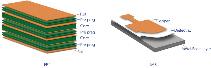
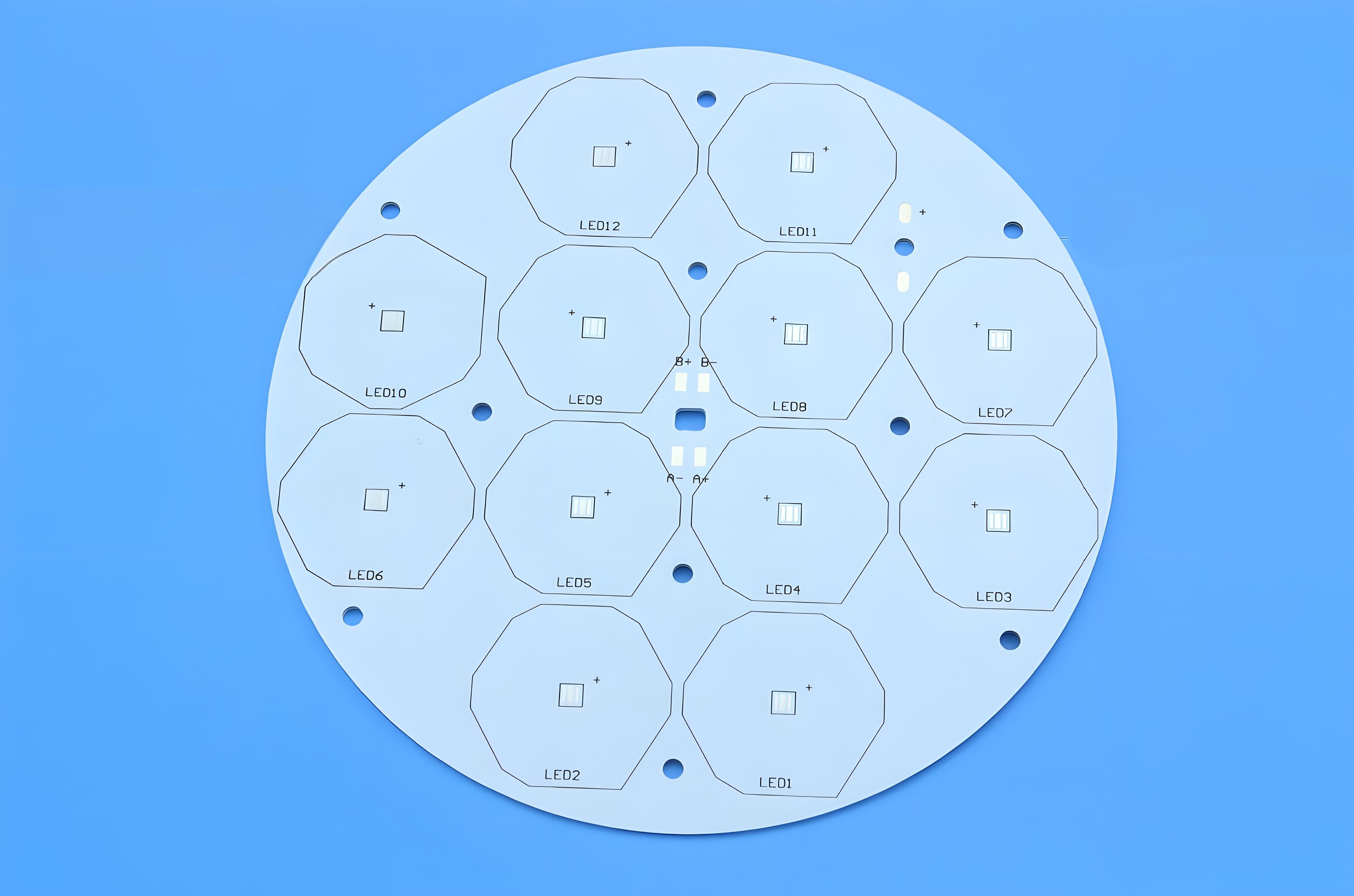
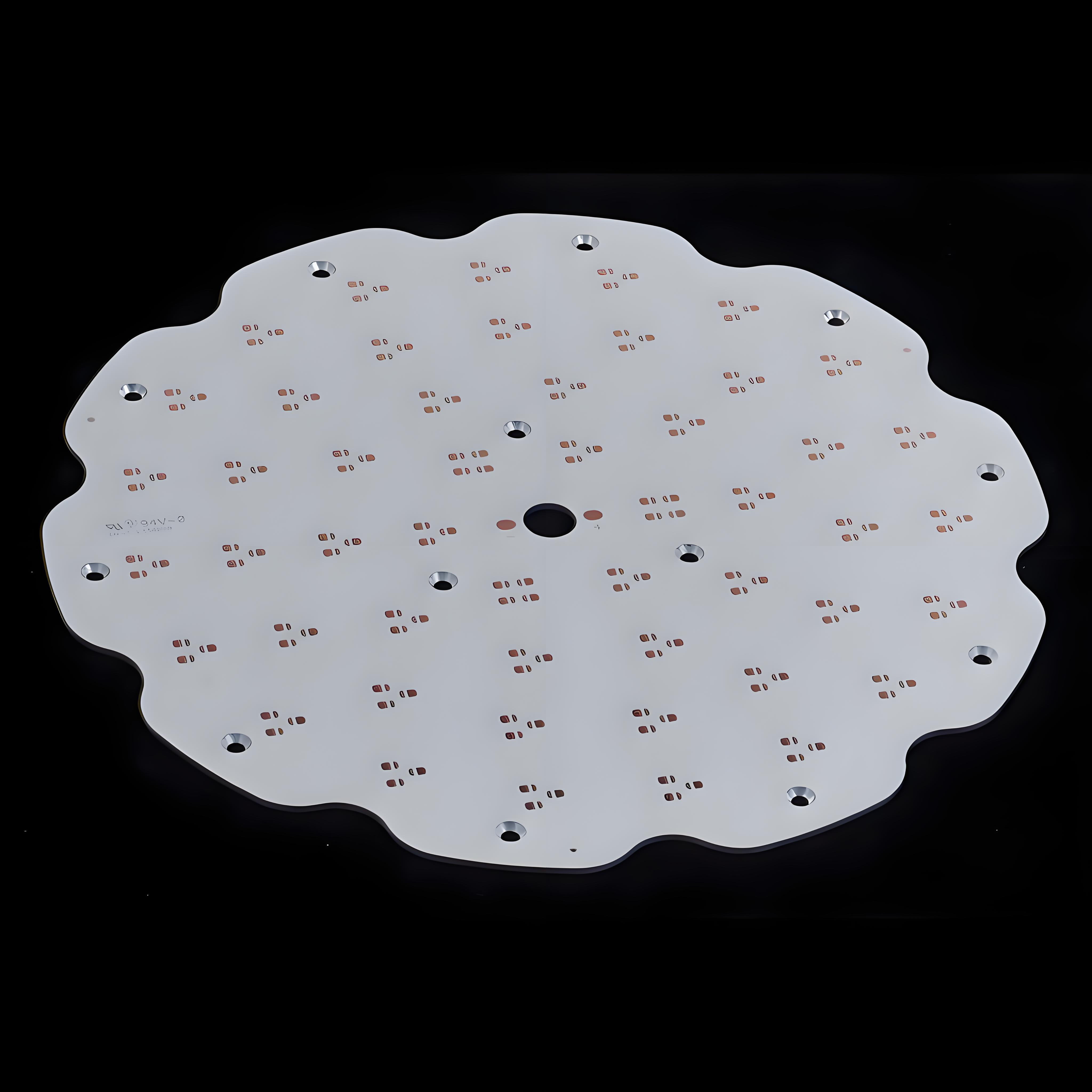
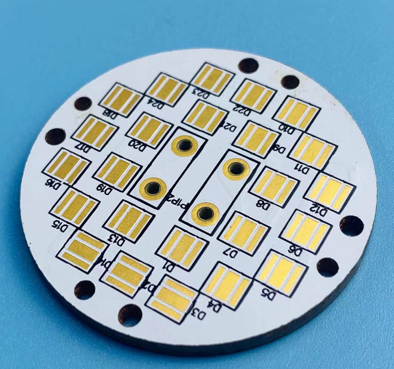
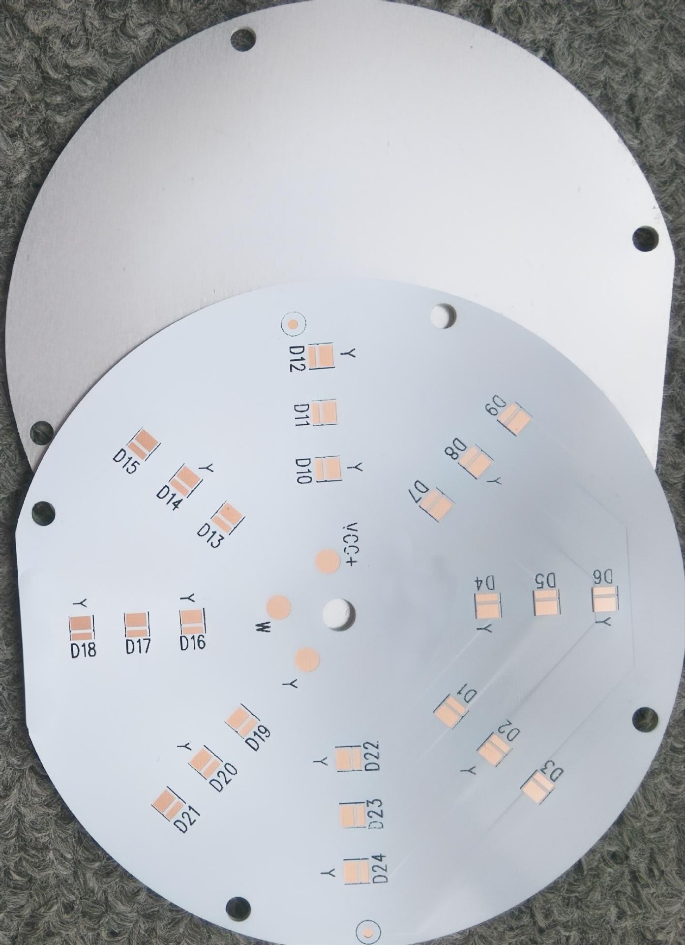
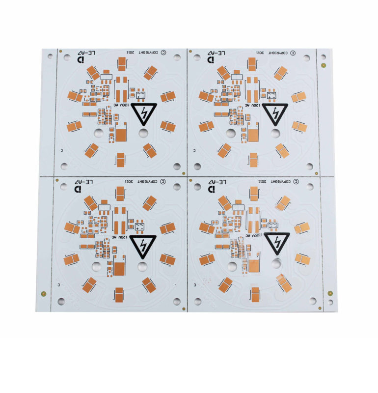
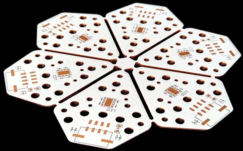
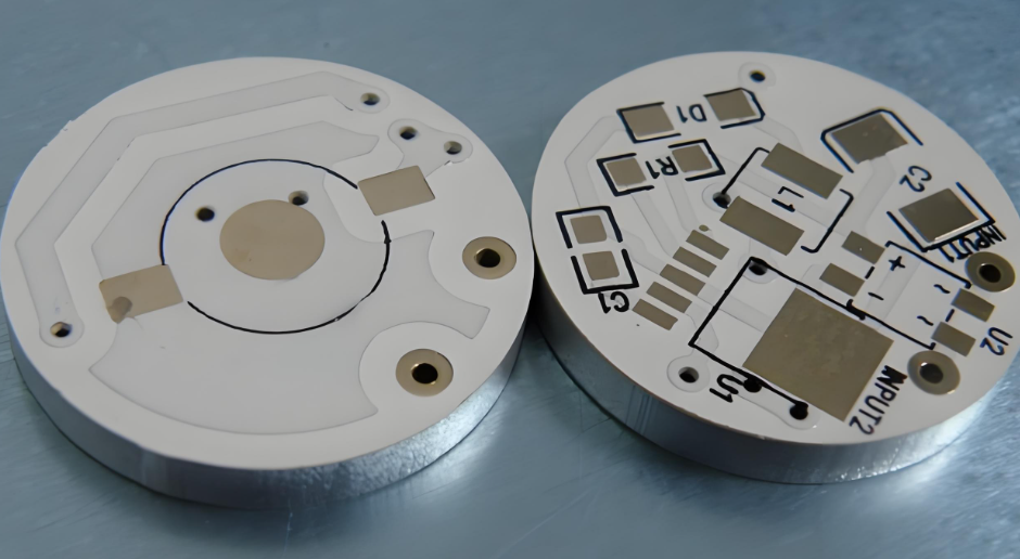
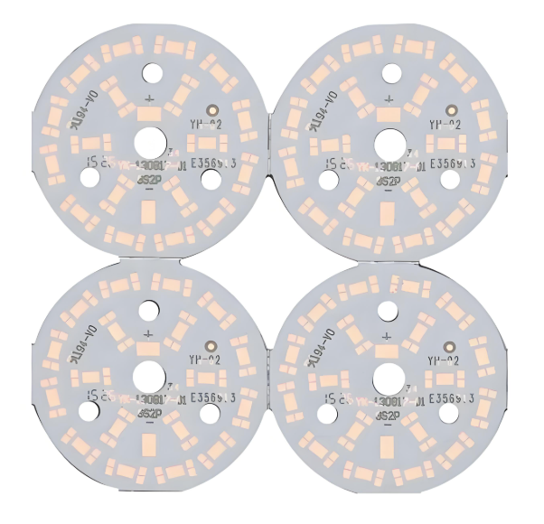
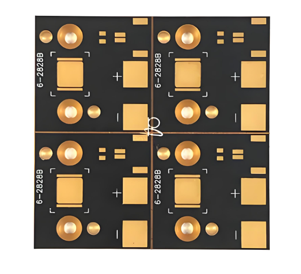
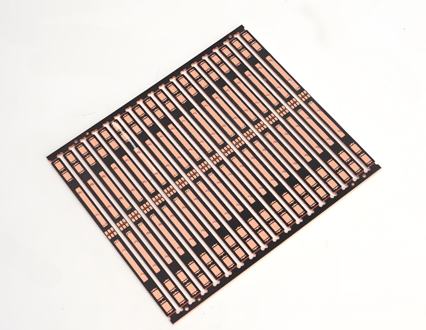
What Is a Double Sided Copper Clad PCB?
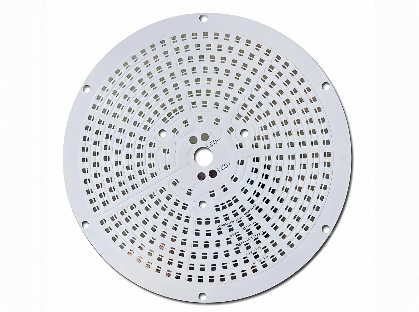
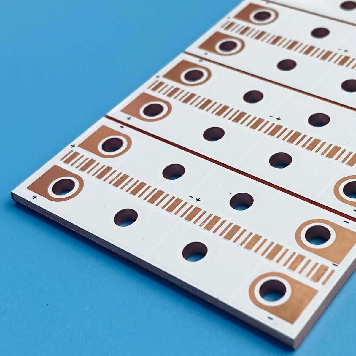
A double sided copper clad PCB is a printed circuit board with conductive copper layers on both top and bottom surfaces of an insulating substrate (typically FR4 or similar material). The copper layers are etched to form circuit patterns, while plated through-holes (PTHs) or vias electrically connect the two sides. This design enables complex circuit routing in compact spaces, making it ideal for applications requiring moderate density interconnections, such as consumer electronics, industrial controls, and power supplies. The structure balances cost efficiency and functional flexibility compared to single-sided or multilayer boards.
What Are Benefits of Double Sided Copper Clad PCB?
Higher Wiring Density
- Double-Sided Copper-Clad PCBs allow traces to be routed on both sides of the board, saving over 50% of space compared to single-sided boards. They are particularly suitable for small and medium-sized electronic devices with complex functions, such as smart wearables and industrial control modules.
Stronger Signal Integrity
- Properly planning double-sided traces shortens high-frequency signal paths, reduces transmission loss, and improves communication stability (e.g., in 5G modules and RF circuits).
Better Cost-Effectiveness
- Compared to multi-layer PCBs, double-sided copper-clad PCBs offer 30%-50% lower manufacturing costs while meeting the performance requirements of most mid-range products, making them the most cost-effective choice.
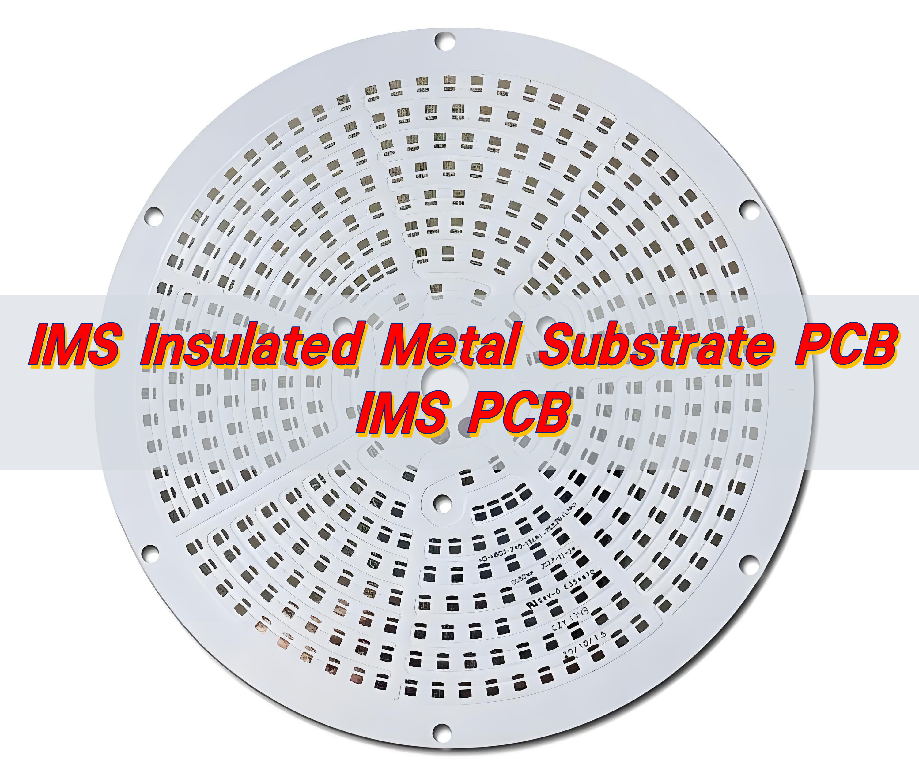
Flexible Thermal Design
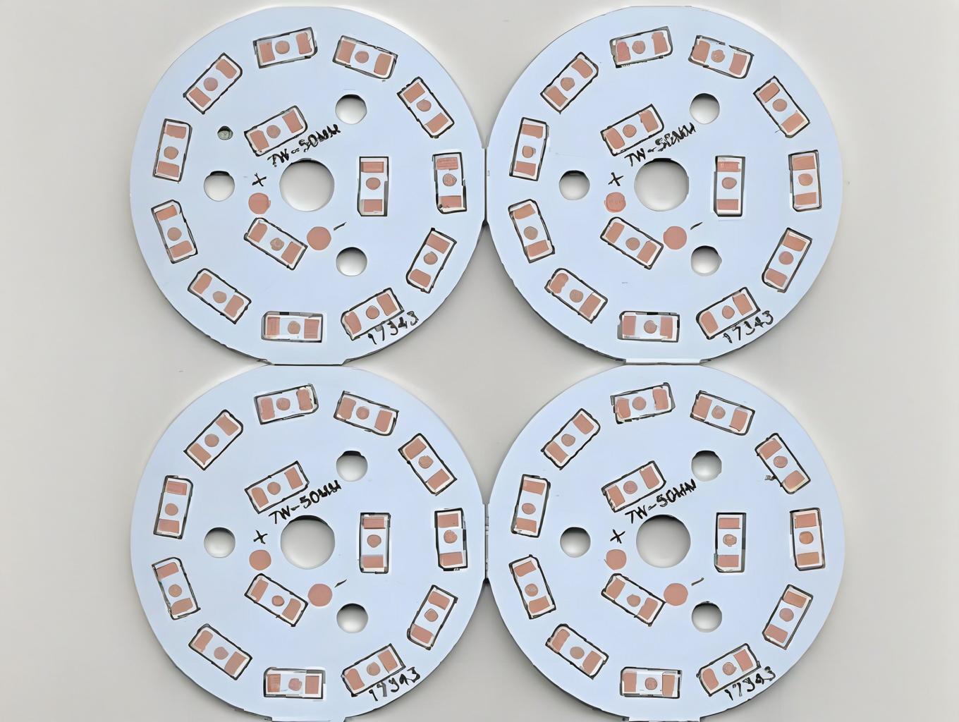
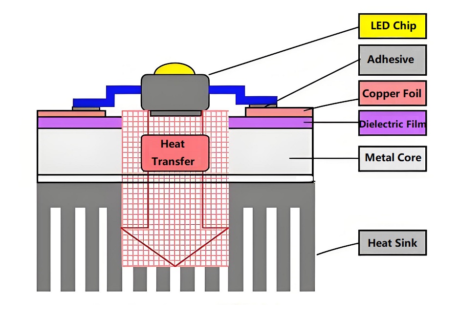
- Using a metal substrate (such as aluminum), the double-sided structure allows for both circuit integration and efficient heat dissipation, making it suitable for applications such as LED lighting and power converters.
Widely Compatible Processes
- Supporting mainstream processes such as through-hole metallization (PTH) and surface mount technology (SMT), they facilitate integration with existing production lines and reduce modification costs.
What Are Applications of Double Sided Copper Base PCB?
- Consumer Electronics – Smartphone motherboards, laptop graphics cards, and tablet devices for compact, high-density wiring.
- Industrial Control – PLC modules, sensors, and motor drivers requiring reliable thermal management and signal integrity.
- Automotive Electronics – Engine Control Units (ECUs), infotainment systems, and battery management for durability in harsh environments.
- Medical Devices – Portable monitors, diagnostic tools, and imaging systems demanding precision and miniaturization.
- Communication Equipment – Routers, switches, and 5G base station modules for efficient signal routing and impedance control.
Difference Between Single and Double Sided Copper Clad PCB
| Comparison Point | Single Sided Copper Clad PCB | Double Sided Copper Clad PCB |
| Copper Layer | 1 layer (bottom side only) | 2 layers (top & bottom) |
| Conduction Method | No vias (jumpers required) | Through-hole vias for interconnections |
| Routing Density | ≤40% utilization (no cross-routing) | ≥70% utilization (cross-routing enabled) |
| Min. Trace/Space | 0.3mm/0.3mm | 0.15mm/0.15mm |
| Thermal Performance | Single-side dissipation (higher Rθ) | Dual-path cooling (30% lower Rθ) |
| Manufacturing Cost | 30-50% lower (simpler process) | 50-80% higher (drilling/plating added) |
| Typical Applications | LED strips/SMPS | IoT devices/Motor drives |
| Signal Integrity | Suitable for <10MHz | Supports ≤100MHz designs |
| Failure Modes | Copper peel-off | Via cracking/Delamination |
| Flexibility | Higher (thinner construction) | Lower (additional structural layers) |
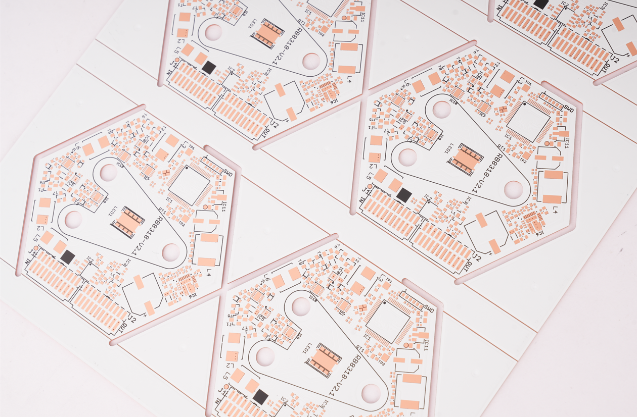
Double Sided Copper Clad PCB Design Guideline
Below is double sided copper clad PCB design guideline:
1. Layout Strategy
- Group analog/digital/power components separately.
- Place critical signals (e.g., clocks, RF) away from board edges.
- Avoid stacking components on opposite sides where possible.
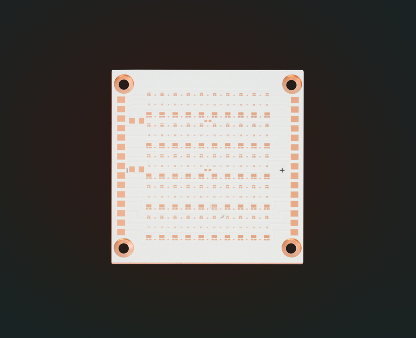
2. Routing Basics
- Use top layer for primary signals; bottom for ground/power planes.
- Keep trace width ≥8 mil (0.2mm) for 1A current.
- Maintain ≥6 mil spacing between traces to reduce crosstalk.
3. Via Best Practices
- Use through-hole vias for layer-to-layer connections.
- Drill size: 0.3–0.5mm (12–20 mil) with ≥0.2mm annular ring.
- Limit via density to <50 per sq. inch to avoid drilling issues.
4. Thermal Considerations
- Add 3–5 thermal vias under high-power components (e.g., MOSFETs).
- Use copper pours (≥70% coverage) on both layers for heat dissipation.
- Connect surface-mount pads to ground planes via thermal relief.
5. Power & Ground Design
- Avoid splitting ground planes unless necessary.
- Place 0.1µF decoupling capacitors near IC power pins.
- Connect analog/digital grounds at a single point (star grounding).
6. Manufacturability Tips
- Add via-based test pads for critical nets.
- Open solder mask ≥0.3mm around pads for wave soldering.
- Check DFM: silkscreen text ≥1mm, avoid acute trace angles.
7. Surface Finish Selection
- Choose HASL for cost-effective through-hole assembly.
- Use ENIG for fine-pitch SMT (e.g., 0.4mm BGA).
8. File Preparation
- Export Gerber layers: top/bottom copper, solder mask, silkscreen.
- Separate NPTH/PTH drill files.
- Include assembly drawings with polarity/orientation marks.
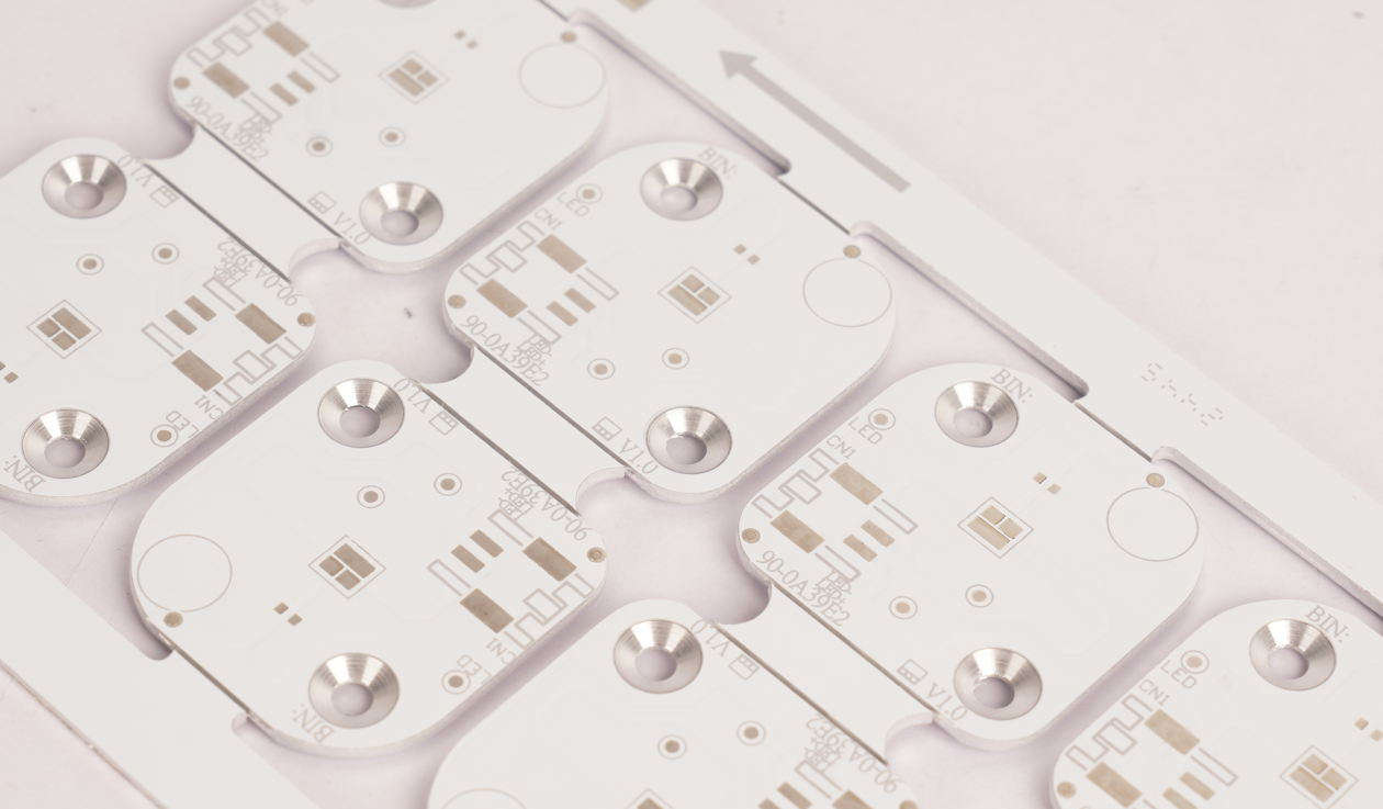
How to Make Double Sided Copper Clad PCB Board?
1. Raw Material Preparation
- Substrate Selection: Use FR-4 (fiberglass-reinforced epoxy) or other flame-resistant materials as the base substrate.
- Copper Foil: Cut copper foils to match the PCB dimensions, ensuring uniform thickness (typically 18–70 µm).
2. Copper Foil Cleaning
- Degrease copper foils using alkaline solutions to remove oils and contaminants.
- Apply micro-etching (e.g., sodium persulfate) to roughen the surface for better adhesion.
3. Lamination Process
- Layer the substrate between two copper foils.
- Use vacuum presses to apply heat (170–200°C) and pressure (20–40 kg/cm²) for 60–120 minutes, bonding the layers.
4. Drilling Holes
- Use CNC drills to create via holes and component mounting holes.
- Deburr holes to remove debris and ensure smooth walls.
5. Electroless Copper Plating (Through-Hole Metallization)
- Immerse the board in a catalyst solution (e.g., palladium chloride) to activate non-conductive holes.
- Deposit a thin layer of copper (0.2–0.5 µm) via chemical plating to connect both sides.
6. Dry Film Photoresist Application
- Laminate dry film photoresist onto both sides of the board.
- Expose the film to UV light through a circuit pattern mask, hardening the exposed areas.
7. Electroplating (Pattern Plating)
- Plate additional copper (20–30 µm) and a tin-lead layer (8–12 µm) over the exposed traces.
- The tin acts as an etch resist during the next step.
8. Etching Process
- Strip the unexposed photoresist using sodium hydroxide.
- Etch away unwanted copper with ammonium persulfate or cupric chloride, leaving the plated traces.
9. Solder Mask Application
- Coat both sides with epoxy-based solder mask ink.
- Expose and develop to retain mask only over non-conductive areas.
10. Surface Finish
- Apply Hot Air Solder Leveling (HASL) for tin-lead coating or OSP (Organic Solderability Preservative) for lead-free options.
11. Electrical Testing
- Use flying probe testers or bed-of-nails fixtures to verify circuit continuity and isolation.
12. Routing/V-Scoring
- Cut individual PCBs from the panel using CNC routers or V-groove scoring for easy separation.
13. Final Inspection & Packaging
- Perform visual checks and dimensional verification.
- Vacuum-seal boards with desiccant packs to prevent moisture damage.
Why Choose EBest Circuit (Best Technology) as Copper Clad PCB Manufacturer?
- Superior Thermal Performance: Copper core delivers 398 W/m·K conductivity, reducing device temperatures by 30% for extended product lifespan.
- Rapid Prototyping Service: 24-hour turnaround for samples with same-day engineering review.
- Competitive Pricing: Transparent pricing with no hidden fees and cost-effective for high-volume production.
- Strict Quality Control: 100% automated optical inspection (AOI) and X-ray testing for defect-free PCBs.
- Fast Production Lead Times: 15-day standard lead time with expedited options for urgent orders.
- Dedicated Engineering Support: 24/7 technical team for design optimization and troubleshooting.
- Free DFM: Optimize your design for manufacturability, reducing production errors by up to 40%.
Our Copper Clad PCB Capabilities
| Base material: | Copper |
| Thermal Conductivity (dielectric layer): | 0.8, 1.0, 1.5, 2.0, 3.0 W/m.K. |
| Board Thickness: | 0.5mm~3.0mm(0.02″~0.12″) |
| Copper thickness: | 0.5 OZ, 1.0 OZ, 2.0 OZ, 3.0 OZ, up to 10 OZ |
| Outline: | Routing, punching, V-Cut |
| Soldermask: | White/Black/Blue/Green/Red Oil |
| Legend/Silkscreen Color: | Black/White |
| Surface finishing: | Immersion Gold, HASL, OSP |
| Max Panel size: | 600*500mm (23.62″*19.68″) |
| Packing: | Vacuum/Plastic bag |
| Samples L/T: | 4~6 Days |
| MP L/T: | 5~7 Days |
Instant Quote
Provide these details for an accurate quote for your metal core PCB project:
- Base Material: Aluminum or copper core (specify thickness, e.g., 1.5mm).
- Copper Thickness: 1-4 oz for outer layers.
- Board Dimensions: Length × width (include tolerance).
- Layer Count: Single-sided or double-sided.
- Surface Finish: HASL, ENIG, or OSP.
- Thermal Requirements: Max operating temperature, heat dissipation targets.
- Special Processes: Via plating, edge plating, or counterbores.
- Quantity: Prototype (1-10 pcs) or bulk order (>100 pcs).
- Lead Time: Standard (7-10 days) or urgent (24-hour prototyping).
Welcome to contact EBest Circuit (Best Technology) at sales@bestpcbs.com if you have any inquiry for metal core PCB.