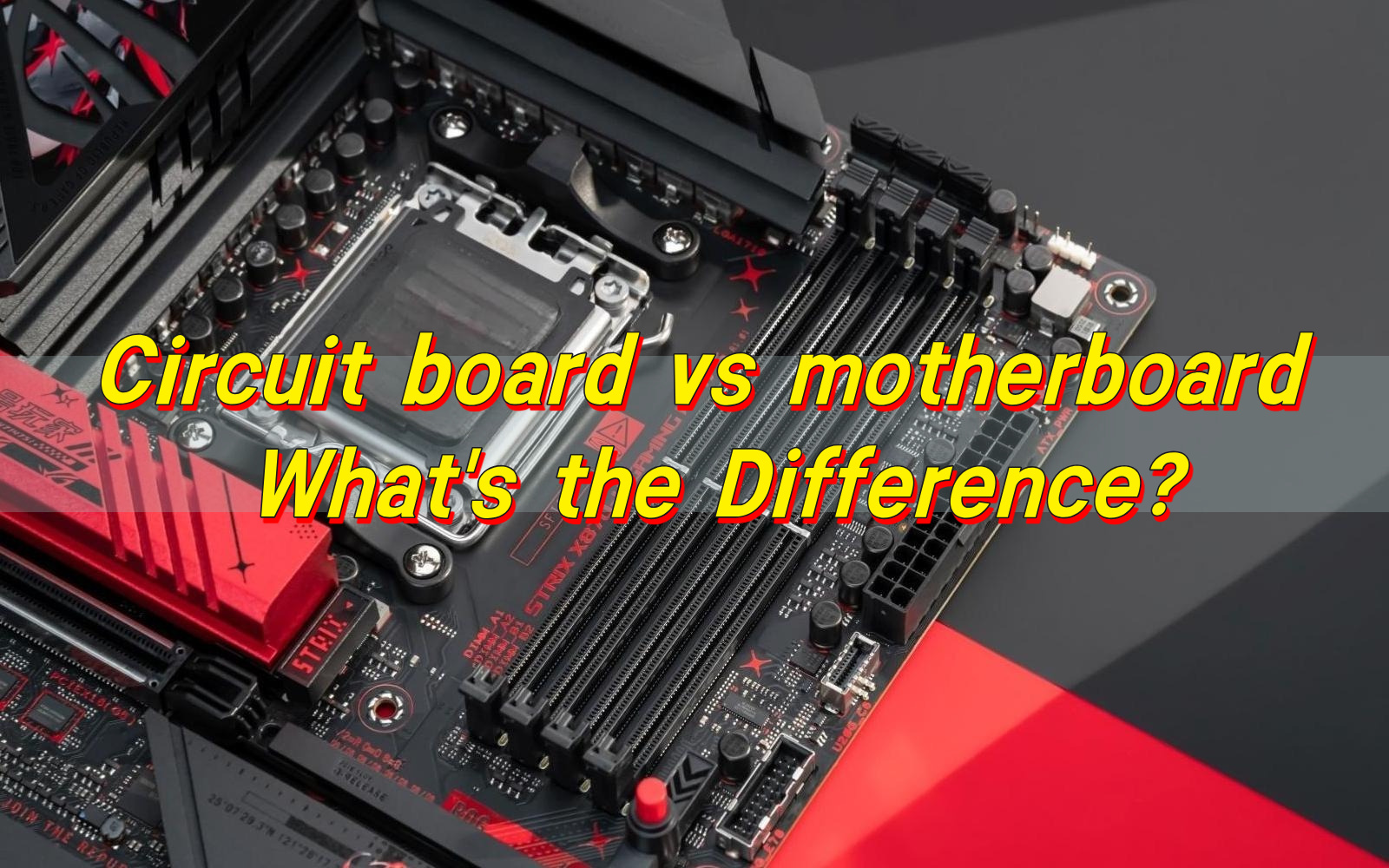
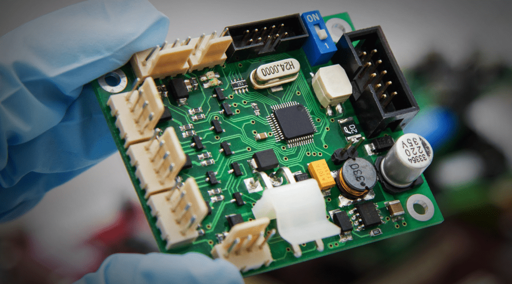
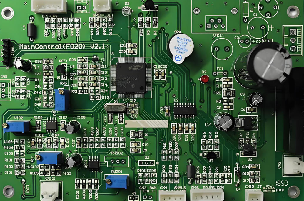
Memahami arti simbol huruf pada papan PCB adalah langkah fundamental untuk setiap profesional elektronik, dari perakitan hingga perbaikan. Setiap simbol huruf pada papan PCB memiliki makna spesifik yang mengidentifikasi jenis komponen, fungsinya, dan posisi, yang memastikan assembler dan teknisi bekerja akurat. Tanpa pengetahuan tentang simbol-simbol ini, Anda berisiko kesalahan assembler, kerusakan komponen, atau keterlambatan proyek. Mari kita bedah secara detail semua hal penting tentang arti simbol huruf pada papan PCB dan cara menggunakannya dengan benar.
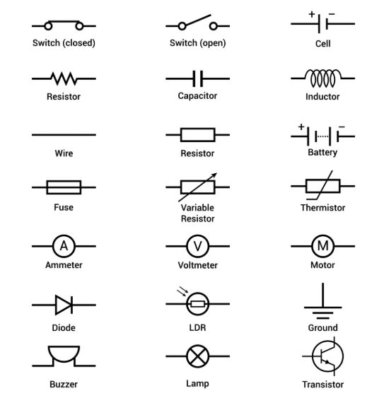
Apa Itu Arti Simbol Huruf Pada Papan PCB?
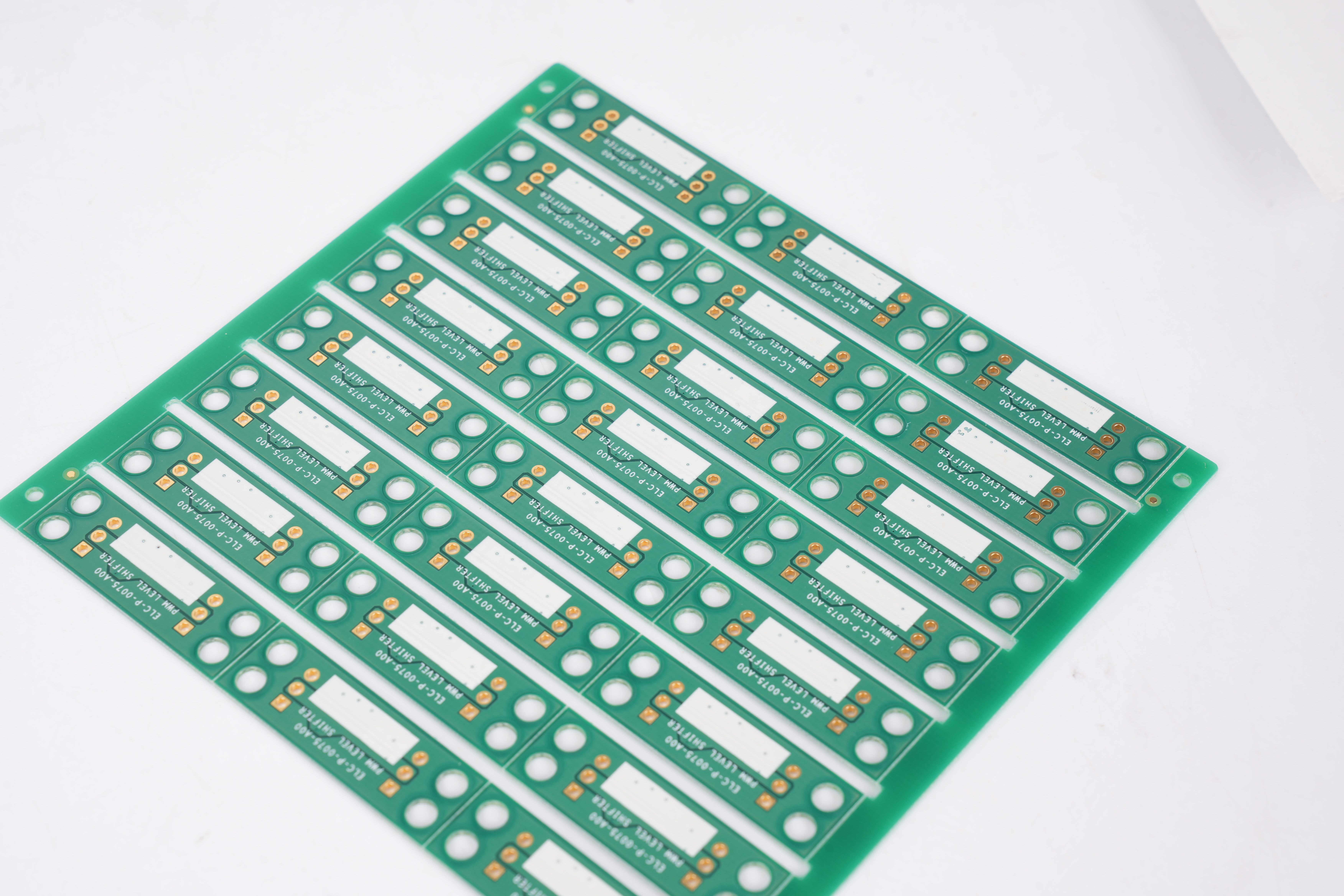
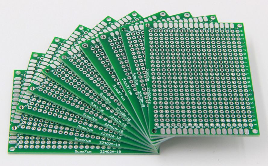
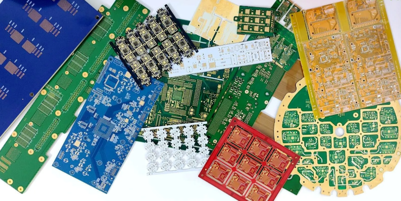
Simbol huruf pada papan PCB, juga disebut identifikasi referensi (RefDes), adalah kode huruf+angka yang dicetak pada lapisan silkscreen papan PCB. Tujuan utamanya adalah mengidentifikasi jenis komponen elektronik secara cepat, memudahkan perakitan, testing, debugging, dan perbaikan. Simbol-simbol ini mengikuti konvensi industri (seperti standar IPC) meskipun ada variasi kecil antar desainer atau perusahaan. Setiap simbol terhubung dengan skema sirkuit dan daftar bahan (BOM) untuk memastikan konsistensi dalam produksi.
Arti Simbol Huruf Pada Papan PCB
100 Common Letter Symbols for Circuit Diagrams
The following symbols cover passive components, active components, power supplies, interfaces, and control signals, complying with general circuit diagram standards.
| No. | Symbol | Component/Function Name | Full English Name |
|---|---|---|---|
| 1 | R | Resistor | Resistor |
| 2 | VR | Variable Resistor | Variable Resistor |
| 3 | POT | Potentiometer | Potentiometer |
| 4 | LDR | Photoresistor | Light-Dependent Resistor |
| 5 | RT | Thermistor | Thermistor |
| 6 | C | Capacitor | Capacitor |
| 7 | CC | Ceramic Capacitor | Ceramic Capacitor |
| 8 | EC | Electrolytic Capacitor | Electrolytic Capacitor |
| 9 | CBB | Polypropylene Capacitor | Polypropylene Capacitor |
| 10 | L | Inductor | Inductor |
| 11 | T | Transformer | Transformer |
| 12 | Z | Impedance | Impedance |
| 13 | F | Fuse | Fuse |
| 14 | FU | Fuse Holder | Fuse Holder |
| 15 | TH | Thermistor Fuse | Thermistor Fuse |
| 16 | D | Diode | Diode |
| 17 | LED | Light-Emitting Diode | Light-Emitting Diode |
| 18 | OLED | Organic LED | Organic Light-Emitting Diode |
| 19 | ZD | Zener Diode | Zener Diode |
| 20 | Q | Transistor | Transistor |
| 21 | NPN | NPN Transistor | NPN Transistor |
| 22 | PNP | PNP Transistor | PNP Transistor |
| 23 | MOSFET | MOS Field-Effect Transistor | Metal-Oxide-Semiconductor Field-Effect Transistor |
| 24 | NMOS | NMOS Transistor | NMOS Transistor |
| 25 | PMOS | PMOS Transistor | PMOS Transistor |
| 26 | JFET | Junction FET | Junction Field-Effect Transistor |
| 27 | SCR | Silicon-Controlled Rectifier | Silicon-Controlled Rectifier |
| 28 | TRIAC | Triac | Triode for Alternating Current |
| 29 | OP-AMP | Operational Amplifier | Operational Amplifier |
| 30 | IC | Integrated Circuit | Integrated Circuit Chip |
| 31 | MCU | Microcontroller | Microcontroller |
| 32 | CPU | Central Processing Unit | Central Processing Unit |
| 33 | GPU | Graphics Processing Unit | Graphics Processing Unit |
| 34 | FPGA | Field-Programmable Gate Array | Field-Programmable Gate Array |
| 35 | RAM | Random Access Memory | Random Access Memory |
| 36 | ROM | Read-Only Memory | Read-Only Memory |
| 37 | EEPROM | Electrically Erasable ROM | Electrically Erasable Programmable Read-Only Memory |
| 38 | V | Voltage Source | Voltage Source |
| 39 | I | Current Source | Current Source |
| 40 | + | Positive Polarity | Positive Polarity |
| 41 | – | Negative Polarity | Negative Polarity |
| 42 | AC | Alternating Current | Alternating Current |
| 43 | DC | Direct Current | Direct Current |
| 44 | GND | Ground | Ground |
| 45 | VCC | Supply Voltage (Collector) | Voltage Common Collector |
| 46 | VDD | Supply Voltage (Drain) | Voltage Common Drain |
| 47 | VEE | Negative Supply Voltage | Voltage Common Emitter |
| 48 | VREF | Reference Voltage | Reference Voltage |
| 49 | B | Battery | Battery |
| 50 | BAT | Battery Pack | Battery Pack |
| 51 | S | Switch | Switch |
| 52 | SW | Slide Switch | Slide Switch |
| 53 | PB | Push Button | Push Button |
| 54 | MS | Mechanical Switch | Mechanical Switch |
| 55 | CTS | Capacitive Touch Switch | Capacitive Touch Switch |
| 56 | K | Relay | Relay |
| 57 | RLY | Electromechanical Relay | Electromechanical Relay |
| 58 | SSR | Solid-State Relay | Solid-State Relay |
| 59 | LS | Light Sensor | Light Sensor |
| 60 | TS | Temperature Sensor | Temperature Sensor |
| 61 | TMP | Temperature Transducer | Temperature Transducer |
| 62 | PIR | Passive Infrared Sensor | Passive Infrared Sensor |
| 63 | MIC | Microphone | Microphone |
| 64 | SPK | Speaker | Speaker |
| 65 | M | Motor | Motor |
| 66 | GM | DC Gear Motor | DC Gear Motor |
| 67 | SG | Servo Motor | Servo Motor |
| 68 | BUZ | Buzzer | Buzzer |
| 69 | ADC | Analog-to-Digital Converter | Analog-to-Digital Converter |
| 70 | DAC | Digital-to-Analog Converter | Digital-to-Analog Converter |
| 71 | VCO | Voltage-Controlled Oscillator | Voltage-Controlled Oscillator |
| 72 | PLL | Phase-Locked Loop | Phase-Locked Loop |
| 73 | OSC | Oscillator | Oscillator |
| 74 | CRY | Crystal Oscillator | Crystal Oscillator |
| 75 | PWM | Pulse Width Modulation | Pulse Width Modulation |
| 76 | USB | Universal Serial Bus | Universal Serial Bus |
| 77 | HDMI | HDMI Interface | High-Definition Multimedia Interface |
| 78 | VGA | Video Graphics Array | Video Graphics Array |
| 79 | LAN | Local Area Network | Local Area Network |
| 80 | WLAN | Wireless LAN | Wireless Local Area Network |
| 81 | RFID | RFID Module | Radio Frequency Identification |
| 82 | RF | Radio Frequency Module | Radio Frequency Module |
| 83 | GPS | Global Positioning System | Global Positioning System |
| 84 | IoT | IoT Module | Internet of Things Module |
| 85 | UART | Universal Asynchronous Receiver-Transmitter | Universal Asynchronous Receiver-Transmitter |
| 86 | SPI | Serial Peripheral Interface | Serial Peripheral Interface |
| 87 | I2C | I2C Bus | Inter-Integrated Circuit Bus |
| 88 | SDA | Serial Data Line | Serial Data Line (I2C Bus) |
| 89 | SCL | Serial Clock Line | Serial Clock Line (I2C Bus) |
| 90 | SCK | Serial Clock | Serial Clock (SPI Bus) |
| 91 | MOSI | Master Output Slave Input | Master Output Slave Input (SPI Bus) |
| 92 | MISO | Master Input Slave Output | Master Input Slave Output (SPI Bus) |
| 93 | SS | Slave Select | Slave Select (SPI Bus) |
| 94 | RX | Receive Pin | Receive Pin (UART/RF) |
| 95 | TX | Transmit Pin | Transmit Pin (UART/RF) |
| 96 | IN | Input | Input Terminal |
| 97 | OUT | Output | Output Terminal |
| 98 | EN | Enable | Enable Signal |
| 99 | RESET/RST | Reset | Reset Signal |
| 100 | INT | Interrupt | Interrupt Signal |
Simbol untuk Konektivitas dan Proteksi
- J, CN, CONN: Konektor (connector). J untuk socket, CN dan CONN untuk konektor umum. Contoh: J1 (header pin), CN3 (USB connector).
- SW, S: Sakelar (switch). SW untuk sakelar geser atau tombol, S untuk sakelar sederhana. Contoh: SW2, S1.
- F, FU: Fuse (sekering). Untuk perlindungan arus berlebih. Contoh: F1, FU2.
- X, Y: Kristal (crystal). Untuk sumber sinyal clock. Contoh: X1 (16MHz crystal), Y2.
Bagaimana Membedakan Simbol Polaritas Pada Papan PCB?
Simbol polaritas pada papan PCB digunakan untuk komponen yang memiliki arah instalasi spesifik, seperti kapasitor elektrolit, dioda, dan IC. Kesalahan polaritas menyebabkan kerusakan permanen pada komponen atau papan PCB.
Simbol Polaritas Umum
- + / –: Digunakan untuk kapasitor elektrolit dan sumber daya. Tanda “+” menunjukkan kutub positif, “-” untuk negatif.
- Solid Dot / Notch (Celah): Pada IC, solid dot atau celah menunjukkan pin 1. Selalu align dengan mark pada body IC.
- Garis Vertikal: Pada dioda, garis vertikal menunjukkan kutub katoda (negative terminal).
Mengapa Simbol Huruf Pada Papan PCB Sering Berbeda Antar Desainer?
Simbol huruf pada papan PCB tidak diatur oleh standar wajib global yang mutlak, melainkan konvensi industri. Perbedaan muncul karena preferensi desainer, perangkat lunak EDA (seperti Altium, KiCad), atau kebutuhan spesifik perusahaan. Misalnya, beberapa desainer menggunakan “T” untuk transformer, sementara yang lain menggunakan “TR”. Beberapa juga menggunakan “K” untuk relay, sedangkan yang lain menggunakan “RL”.
Untuk mengatasi ini, selalu referensikan skema sirkuit dan BOM yang disediakan oleh tim desain. Dokumentasi ini adalah sumber informasi paling akurat dibandingkan hanya mengandalkan simbol huruf pada papan PCB.
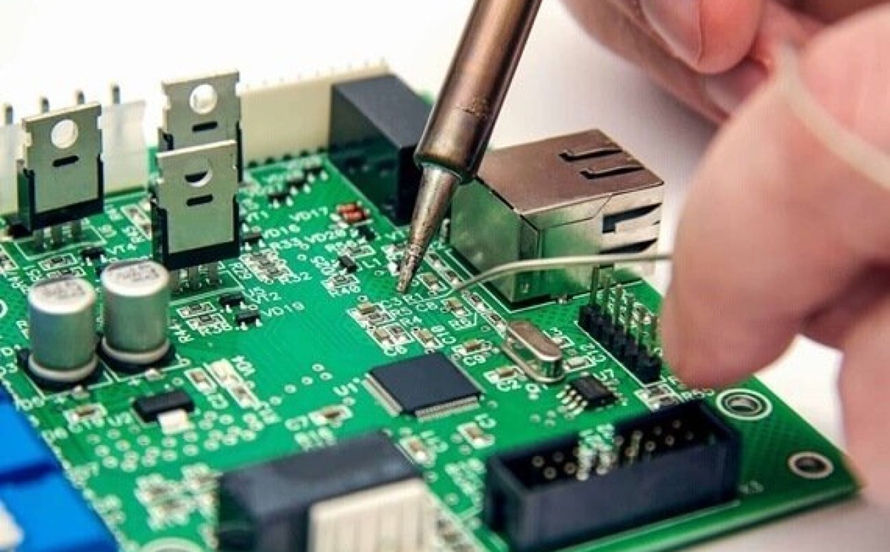
Bagaimana Cara Membaca Simbol Huruf Pada Papan PCB dengan Benar?
Langkah-langkah Praktis
- Identifikasi Huruf Awal: Huruf pertama menunjukkan jenis komponen (contoh: R = resistor, U = IC).
- Perhatikan Nomor Urut: Nomor setelah huruf menunjukkan posisi komponen (contoh: R1 adalah resistor pertama, R2 adalah resistor kedua).
- Hubungkan dengan Skema: Cocokkan simbol dengan skema sirkuit untuk mengetahui fungsi komponen dalam sirkuit.
- Check BOM: Daftar bahan (BOM) memberikan detail spesifikasi komponen (nilai resistor, model IC) yang sesuai dengan simbol.
Apa Saja Kesalahan Umum dalam Memahami Simbol Huruf Pada Papan PCB?
Kesalahan yang Harus Dihindari
- Mengabaikan Variasi Simbol: Anggap semua simbol mengikuti standar tunggal, menyebabkan kesalahan instalasi (misal: mengira “K” adalah sakelar padahal relay).
- Ignor Polarity Mark: Tidak memperhatikan tanda polaritas pada kapasitor elektrolit atau IC, menyebabkan kerusakan.
- Hanya Mengandalkan Simbol Tanpa Skema: Tanpa skema, sulit memastikan fungsi komponen, terutama pada papan PCB kompleks.
- Kesalahan dalam Membaca Nomor Urut: Menukar R1 dengan R10, yang dapat mengubah karakteristik sirkuit.
FAQ Tentang Arti Simbol Huruf Pada Papan PCB
FAQ
Apa yang terjadi jika saya salah memasang komponen berdasarkan simbol huruf?
Kesalahan instalasi berdasarkan simbol huruf dapat menyebabkan berbagai masalah, dari sirkuit tidak berfungsi hingga kerusakan permanen pada komponen atau papan PCB. Misalnya, memasang dioda dengan polaritas terbalik akan mencegah arus mengalir dengan benar, sementara memasang IC dengan pin 1 salah dapat merusak chip secara permanen.
Apakah simbol huruf pada papan PCB sama untuk semua jenis papan?
Tidak sama secara mutlak, tetapi ada konvensi umum yang diikuti industri. Papan PCB untuk otomotif, medis, atau elektronik konsumen menggunakan simbol yang mirip, tetapi ada variasi kecil sesuai kebutuhan spesifik industri. Selalu periksa dokumentasi proyek untuk memastikan akurasi.
Bagaimana jika simbol huruf pada papan PCB hilang atau buram?
Jika simbol hilang atau buram, gunakan skema sirkuit dan BOM sebagai referensi utama. Anda juga bisa menggunakan alat pengukur (multimeter) untuk mengidentifikasi jenis komponen secara manual, meskipun ini membutuhkan pengetahuan teknis yang cukup. Untuk papan PCB massal, hubungi pabrikan untuk mendapatkan salinan skema.
Apakah ada standar resmi untuk simbol huruf pada papan PCB?
Standar yang paling umum diikuti adalah standar IPC (Association Connecting Electronics Industries), terutama IPC-2221 yang mengatur desain papan PCB. Selain itu, IEEE juga memiliki panduan untuk identifikasi komponen, tetapi kedua standar ini bersifat rekomendatif, bukan wajib. Perusahaan dapat membuat variasi sesuai kebutuhan internal.
Bagaimana cara memastikan simbol huruf pada papan PCB jelas dan terbaca?
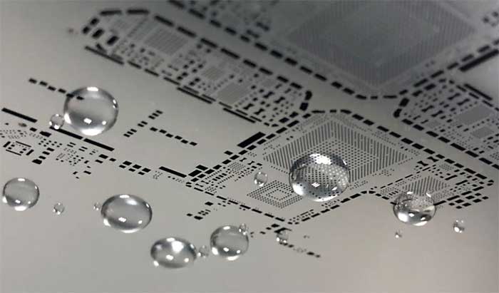
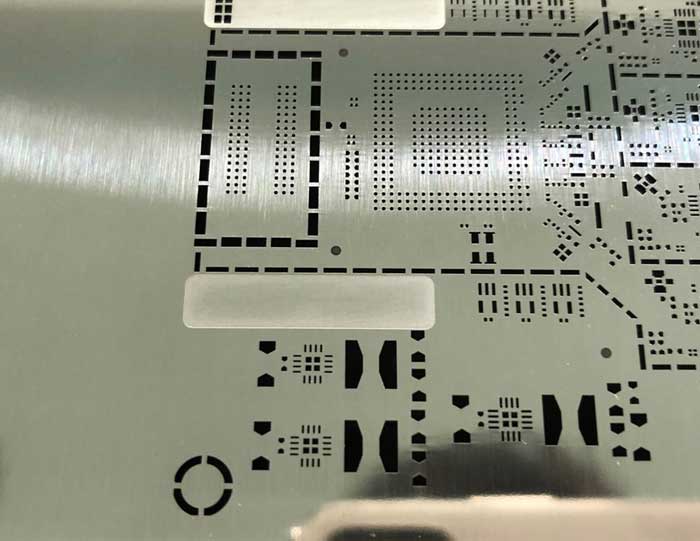
Untuk memastikan simbol jelas, pastikan desain silkscreen menggunakan ukuran font yang cukup (minimal 1.0mm tinggi dan 0.15mm lebar garis), menghindari penutupan pads atau via, dan menggunakan warna ink yang kontras dengan warna papan PCB (putih pada papan hijau adalah kombinasi paling umum). Selalu test cetak prototipe sebelum produksi massal.
Bagaimana Desain Simbol Huruf Mempengaruhi Kualitas Papan PCB?
Desain simbol huruf yang baik meningkatkan efisiensi produksi dan mengurangi risiko kesalahan assembler. Simbol yang jelas dan teratur memungkinkan assembler bekerja lebih cepat, mengurangi waktu siklus produksi. Sebaliknya, simbol yang buram, tumpang tindih, atau tidak jelas meningkatkan biaya rework dan risiko cacat produk.
Selain itu, simbol yang sesuai standar juga memudahkan perbaikan dan maintenance di masa depan, yang meningkatkan nilai jangka panjang papan PCB.
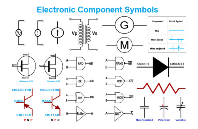
Apa Perbedaan Antara Simbol Huruf dan Simbol Grafis Pada Papan PCB?
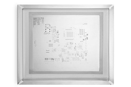
Simbol huruf adalah kode huruf+angka yang mengidentifikasi jenis komponen, sedangkan simbol grafis adalah gambar atau bentuk yang menunjukkan outline komponen atau arah instalasi. Misalnya, simbol grafis untuk IC adalah kotak dengan solid dot (pin 1), sedangkan simbol hurufnya adalah U1. Simbol grafis membantu assembler memposisikan komponen secara visual, sementara simbol huruf mengidentifikasi jenisnya.
Tips Memilih Papan PCB dengan Simbol Huruf yang Akurat
Saat memesan papan PCB, pastikan vendor menyediakan layanan silkscreen yang berkualitas. Periksa prototipe untuk memastikan simbol huruf jelas, tidak tumpang tindih, dan sesuai dengan desain Gerber. Jelaskan kebutuhan simbol polaritas dan identifikasi khusus jika proyek Anda membutuhkannya. Pilih vendor yang mematuhi standar IPC untuk memastikan konsistensi kualitas.
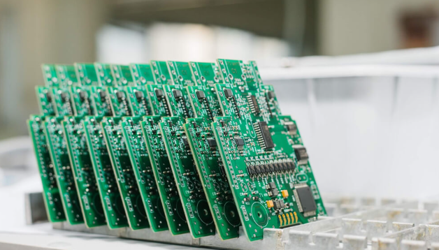
EBest menyediakan layanan produksi papan PCB dengan desain simbol huruf akurat dan berkualitas, sesuai standar industri. Kami memastikan setiap arti simbol huruf pada papan PCB dicetak dengan jelas, memudahkan perakitan dan maintenance proyek Anda. Jika Anda membutuhkan papan PCB dengan simbol huruf yang akurat dan andal, silakan kirimkan inquiry ke sales@bestpcbs.com untuk mendapatkan penawaran terbaik.