How to design high speed circuit boards? Let’s discover design guidelines, impedance control technical parameter, layout guide, impedance matching and verification for high speed circuit boards.
Are you worried about these problems?
- Impedance out of control causing eye diagram collapse?
- Differential pair spacing exceeding ±2mil?
- Simulation vs. measurement discrepancy >5%?
As a high speed circuit boards manufacturer, EBest Circuit (Best Technology) can provide you service and solution:
- Free DFM analysis + precise impedance design: Achieve 50Ω single-ended ±10% and 100Ω differential ±10% on first pass.
- 24-hour rapid response: Provide manufacturability optimization feedback based on Gerber files, reducing trial production losses by 30%.
- Full-chain verification: Identify via stubs, bends, and other defects early via TDR/eye diagram analysis, accelerating mass production ramp-up.
Welcome to contact us if you have any request for high speed circuit boards: sales@bestpcbs.com.
High Speed Circuit Boards Design Guidelines
Below are high speed circuit boards design guidelines:
1. Manufacturability Requirements
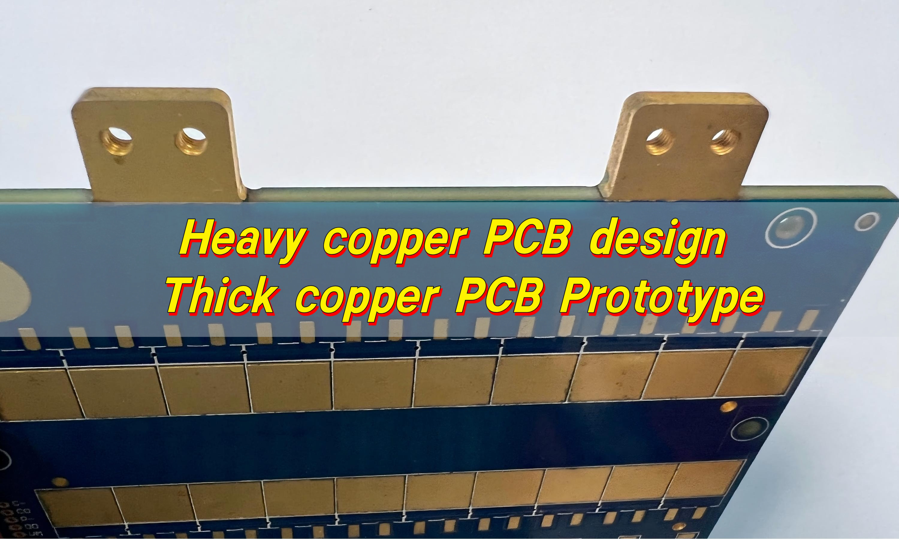
- Specify board thickness (e.g., 1.6mm), copper thickness (e.g., 1oz), and surface finish (e.g., ENIG).
- Define SMD/through-hole pad dimensions, solder mask openings, and stencil specifications.
- Verify impedance control parameters through production testing (e.g., TDR measurements).
- Reserve test points for high-speed interfaces (e.g., HDMI, PCIe) to facilitate debugging.
2. Multilayer Stackup Structure
- Use a minimum of 4-layer structure, with 6 or more layers recommended for optimal performance.
- Implement continuous ground and power planes to minimize signal return path discontinuities.
- Select low-loss dielectric materials (e.g., FR4 for cost-effectiveness, Teflon for ultra-high-speed applications).
- Document stackup specifications including board thickness (typically 1.6mm), copper weight (e.g., 1oz), and blind/buried via requirements in design files.
3. Component Placement Strategy
- Prioritize placement of high-speed signal transmitters/receivers near their respective signal paths.
- Adopt grid-based layouts to minimize signal trace lengths and cross-talk risks.
- Position decoupling capacitors within 0.2mm of power pins to suppress power noise.
- Keep critical components at least 3mm away from board edges and connectors to avoid mechanical stress and EMI interference.
4. Impedance Control Implementation
- Design all high-speed traces to target impedance (typically 50Ω single-ended, 100Ω differential).
- Ensure traces reference a continuous ground plane—top/bottom layers use single-sided referencing, inner layers use dual-sided.
- Avoid crossing plane splits or board edges to maintain consistent impedance and reduce signal reflections.
- Maintain strict parallelism and same-layer routing for differential pairs to ensure coupling integrity.
5. Signal Routing Specifications
- Replace 90° bends with 135° bends to reduce capacitance discontinuities.
- Maintain trace spacing ≥3× line width (3W rule) to minimize cross-talk.
- Control intra-pair and inter-pair length mismatches to ≤500μm for high-speed signals.
- Use serpentine traces only in length-mismatch regions to equalize delays without introducing noise.
- Avoid long stubs; prefer daisy-chain topologies for signal integrity.
6. Noise Suppression Measures
- Apply termination resistors (source or load) to match transmission line impedance.
- Cover high-speed signal regions with ground planes to shield against EMI.
- Implement π-type filters on power rails to suppress high-frequency noise.
- Minimize ground loop area to reduce inductive coupling and radiated emissions.
7. Via and Interconnect Design
- Limit via counts on high-speed paths to reduce parasitic capacitance/inductance.
- Place ground/power vias adjacent to component pads for low-impedance connections.
- For BGA packages, use Via-in-Pad with filled vias to minimize pad size and improve thermal management.
- Ensure vias reference adjacent ground planes to maintain return path continuity.
8. Design Rule Documentation
- Define differential pair parameters (e.g., pair spacing, trace width), routing topologies, and length tolerances.
- Include manufacturing annotations such as impedance-controlled trace widths/spacing and stackup details.
- Add ≥3 optical fiducial markers for precise assembly alignment.
- Adhere to IPC Class 3 standards for reliability in high-performance applications.
9. Simulation and Validation Workflow
- Annotate high-speed signal constraints (e.g., impedance, length) in schematics.
- Perform pre-layout signal integrity simulations (TDR for impedance, eye diagrams for signal quality).
- Validate return path continuity through ground plane checks.
- Compare crosstalk models with actual layouts to identify and mitigate coupling issues.
High Speed Circuit Boards Impedance Control Design Technical Parameter
| Parameter | Value Range/Requirements |
| Single-Ended Signal Impedance | 50Ω ±10% (typical) |
| Differential Signal Impedance | 100Ω ±10% (per leg) or 90Ω ±10% |
| Special Interface Impedance | 75Ω (analog video), 85Ω (custom interfaces) |
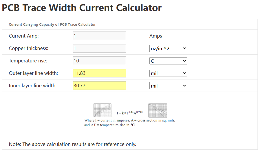
| Trace Width (W) | 5-10mil (single-ended); 6-16mil (differential) |
| Trace Spacing (S) | ≥3× trace width (3W rule); differential spacing 5-10mil |
| Differential Pair Spacing | Strict parallel, same-layer routing, tolerance ≤±2mil |
| Board Thickness (H) | 1.6mm ±10% (standard); 0.8-3.0mm (custom) |
| Copper Thickness (T) | 0.5oz (17μm), 1oz (35μm), 2oz (70μm) |
| Dielectric Thickness (H1/H2) | Microstrip: signal-to-reference distance; stripline: core/prepreg thickness |
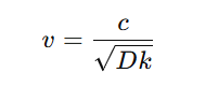
| Dielectric Constant (Dk) | FR4: 4.2-4.7 (typical 4.4); high-frequency materials (e.g., Rogers): 3.5-4.0 |
| Loss Tangent (tanδ) | FR4: 0.015-0.025; low-loss materials: ≤0.005 |
| Reference Plane Continuity | Continuous ground/power plane under signal traces; avoid splits |
| Ground Shield Design | Ground trace ≥20mil wide, 6mil spacing, via every 400mil |
| Shield Ground Distance | ≥35mil from differential signals (≥20mil in special cases) |
| Via Count Limitation | Minimize vias on high-speed paths; use backdrilling if needed (stub length ≤10% board thickness) |
| Via Reference Plane | Adjacent to ground plane for continuous return path |
| Solder Mask Thickness | 0.6±0.2mil, dielectric constant 3.5±0.3 |
| Surface Finish | ENIG, HASL, etc.; evaluate impact on impedance |
| Impedance Measurement | TDR testing, tolerance ±5% to ±10% |
| Simulation Verification | Signal integrity simulation, TDR/eye diagram analysis |
| Trace Bend Angle | 135° or radius transition; avoid 90° right angles |
| Length Matching Accuracy | Differential pair length mismatch ≤500μm (±3mil) |
| Crosstalk Control | ≥3× trace width spacing; prefer daisy-chain topology |
Ground Plane Impedance Management Techniques for High Speed Board
Mandatory Standards for Ground Plane Continuity
- All ground planes beneath high-speed signal paths must remain intact without mechanical segmentation. For unavoidable digital/analog ground segmentation, use 0603-sized 0Ω resistors to bridge gaps with spacing ≤3mm, ensuring a low-impedance path ≤10mΩ.
Quantitative Layout Specifications for Via Arrays
- Each high-speed signal via must be surrounded by four symmetrically placed ground vias in a rhombus array, with spacing strictly controlled at 2.5–3mm. For differential pairs, adopt an “8-12” array (8 signal vias paired with 12 ground vias) to maintain coupling coefficients ≥0.8.
Copper Thickness-Frequency Mapping Table
- Establish a direct correlation between copper thickness and signal frequency: ≤500MHz uses 1oz copper; 500MHz–2GHz uses 1.5oz copper; ≥2GHz requires 2oz copper. Measurements confirm 2oz copper reduces 1GHz ground impedance by 35% and temperature rise by 40%.
3D Layout Method for Decoupling Capacitors
- Within 3mm of IC power pins, implement “capacitor stacking”: place 100μF electrolyytic capacitors on the bottom layer and 0.1μF/0.01μF ceramic capacitors on the top layer. Ground terminals connect to the ground plane via ≥6 vias with spacing ≤1mm.
Length Control Standards for Ground Paths
- Ground path lengths for critical signals (e.g., DDR clocks) must be ≤1/20 of the signal wavelength. Validate with TDR measurements, ensuring path length errors within ±0.5mm and ground impedance ≤5mΩ.
Compensation Capacitor Matrix for Segmented Areas
- For digital/analog ground segmentation zones, deploy two 100nF/50V X7R capacitors per 100mm² area. Install capacitors in “back-to-back” configuration with connection points straddling segmentation seams, creating equivalent capacitance ≥200nF.
Closed-Loop Impedance Measurement & Optimization
- Measure ground impedance from 1kHz to 3GHz using a network analyzer. For out-of-spec frequencies (e.g., >10mΩ), apply localized copper thickening (to 3oz) or add 1–2 10μF tantalum capacitors. Re-test after optimization to ensure smooth impedance curves without peaks.
Integrated Thermal-Ground Design Template
- For components with power >1W, implement a 2oz copper heat dissipation zone beneath the device. Connect to ground plane via ≥4 thermal vias (diameter ≥0.3mm) filled with conductive silver paste, ensuring thermal resistance ≤15°C/W.
Impedance Control Design Strategies for High Speed Circuit Boards
Standardized Stackup Structure Design Process
- Enforce a 6-layer architecture: “Signal-Ground-Power-Signal-Power-Ground” with dielectric constant strictly controlled at 4.2±0.2 and copper thickness 1.4mil.
- Use ANSYS SIwave for interlayer coupling capacitance simulation, generating impedance error heatmaps for 50Ω paths. Error ≤±5% must cover ≥90% of critical paths.
- Material thickness locked at 8-10mil; verify copper thickness uniformity (±0.2mil) and layer alignment accuracy ≤50μm via microsection analysis.
3D Quantitative Specifications for Differential Pair Routing
- All high-speed differential pairs must follow “6mil trace width/6mil spacing” tight coupling standard, with differential impedance controlled at 100±10Ω.
- Via stub length hard-limited to ≤5mil; validate via TDR measurements to ensure crosstalk coefficient ≤3% between differential pairs.
- At layer transitions, enforce “ground via arrays”: 4 symmetrically placed ground vias (spacing 2.5-3mm) around each signal via.
Closed-Loop Verification via Impedance Calculation Toolchain
- Use Polar SI9000 for impedance calculation: input material parameters (Dk=4.2, Df=0.015) to generate impedance curves.
- For critical paths, implement dual “measured-calculated” validation: TDR-measured impedance vs. calculated curves. Trigger design iteration if error >±8% (max 2 iterations).
3D Quantitative Standards for Decoupling Capacitor Placement
- Within 3mm of CPU/FPGA power pins, implement “capacitor stacking”: bottom-layer 100μF electrolyytic + top-layer 0.1μF ceramic capacitors.
- Each capacitor connects to ground via ≥6 vias (spacing ≤1mm), achieving ≤5mΩ ground impedance.
- Enforce 40dB power noise suppression ratio, validated via spectrum analyzer measurements.
Standardized Design Specifications for Impedance Test Points
- Deploy SMA-connector test points on critical paths (e.g., DDR/PCIe) with spacing ≤50mm.
- Validate 1GHz impedance via network analyzer: error ≤±5Ω; auto-generate and archive test reports.
- Material Selection and Process Binding Execution Details
- For signals ≤2GHz: FR4 (Dk=4.2); ≥2GHz: RO4350B (Dk=3.48).
- Material thickness controlled at 8-10mil; verify copper uniformity (±0.2mil) via microsection.
- High-speed signal vias require backdrilling: stub length ≤3mil, validated via X-ray inspection.
Automated DRC Enforcement for Routing Rules
- Use Altium Designer DRC: enforce 4mil/4mil min trace/space and ≤5mil via stubs.
- For critical paths, enable “serpentine delay difference” checks to ensure signal delay difference ≤5ps; auto-generate DRC reports.
Execution Standards for Power Integrity Co-Design
- PDN design must include decoupling capacitor layout diagrams + power plane segmentation specs.
- For noisy areas (e.g., CPU vicinity), implement “power plane voiding + filter capacitors” to suppress noise ≤100mV.
Closed-Loop Impedance Validation Process
- After simulation, prototype PCBs and measure impedance.
- For out-of-spec points (e.g., >55Ω), apply localized copper thickening (to 2oz) or add capacitors; re-test until compliant.
DFM Binding Execution Details
- Provide IPC-6012-compliant DFM reports including min annular ring, drill parameters, and solder mask dimensions.
- High-speed signal vias require backdrilling (stub ≤3mil), validated via X-ray inspection.
A Practical Guide to High Speed Printed Circuit Board Layout
1. Component Placement Priority
- Place high-speed signal drivers/receivers (e.g., SERDES chips, RF amplifiers) within 5mm of connectors/signal entry points to minimize trace length.
- Keep sensitive analog/high-speed sections ≥3mm from board edges and mechanical stress zones (e.g., mounting holes) to prevent EMI leakage and physical damage.
2. Grid-Based Routing System
- Use 50-100mil grid spacing for component alignment to standardize trace paths and reduce cross-talk.
- Replace 90° bends with 135° arcs or smooth curves in high-speed traces to minimize capacitance discontinuities (e.g., for DDR/PCIe signals).
3. Decoupling Capacitor Strategy
- Position 0.1μF ceramic capacitors within 0.2mm of high-speed IC power pins; use 10μF bulk capacitors within 5mm for broadband noise suppression.
- Connect capacitors directly to ground via low-impedance paths (≤1mm trace length) with dedicated ground vias.
4. Controlled Impedance Routing
- Route high-speed signals (e.g., HDMI, USB3.0) with 50Ω single-ended/100Ω differential impedance, using trace widths/spacing calculated via EDASoft Impedance Calculator.
- Limit high-speed path vias to ≤2 per signal; use backdrilling for stubs >500μm to reduce reflections.
5. Differential Pair Precision
- Maintain differential pair spacing ≤±2mil with strict parallelism on the same layer (e.g., for Ethernet/LVDS).
- Use serpentine meandering only for length compensation (≤500μm mismatch), with loops perpendicular to signal flow to minimize coupling noise.
6. Ground Plane Integrity
- Implement continuous copper ground planes beneath high-speed signal traces (layer-specific, e.g., Layer 2 for top-layer signals).
- Avoid splitting ground planes under high-speed traces; use moats (cut planes) only with bypass capacitors for isolation.
7. Thermal Management Integration
- Position high-power components (e.g., power regulators) away from high-speed sections by ≥10mm.
- Use thermal vias (≥5 vias per pad) for BGA/QFN packages, ensuring via spacing ≥0.8mm to avoid signal integrity degradation.
8. Board Edge Clearance & Shielding
- Maintain ≥3mm clearance between high-speed traces and board edges/connectors.
- Add ground stitching vias (spacing ≤5mm) along board edges with 20mil ground traces spaced 6mil from signals for EMI containment.
9. Length Matching & Tolerance Control
- Ensure intra-pair/inter-pair length mismatches ≤500μm (±3mil) for high-speed signals (e.g., DDR4 DQ groups).
- Use meandering in non-critical sections only, with loop width ≥3× trace width to avoid noise injection.
10. Isolation & Shielding Techniques
- Surround high-speed signal regions with ground traces (≥20mil width) spaced 6mil from signals, adding ground vias every 400mil.
- Isolate analog/digital sections using moats (cut ground planes) with 10nF bypass capacitors to prevent noise coupling.
Signal Path Impedance Matching Practices in High Speed Circuit Boards
1. Precise Target Impedance Setting
- Single-ended signals adopt a standardized 50Ω±10% impedance, suitable for high-speed digital scenarios such as DDR control lines and clock signals.
- Differential pairs use 100Ω±10% (per leg) or 90Ω±10% impedance to match standards like HDMI, USB, and PCIe.
- Special interfaces (e.g., analog video) require 75Ω impedance, while custom interfaces adjust to 85Ω or other values based on device specifications.
2. Refined Trace Parameter Control
- Single-ended trace widths are controlled between 5-10mil, and differential pair widths between 6-16mil. Exact values are determined via EDA tools considering board thickness, copper weight, and dielectric constant.
- Trace spacing follows the 3W Rule (≥3× trace width), with differential pairs maintaining strict parallelism and same-layer routing at 5-10mil spacing, tolerance ≤±2mil to prevent impedance mismatch.
3. Reference Plane Continuity Assurance
- A continuous ground/power plane is laid beneath high-speed signal traces, single-sided referencing for top/bottom layers, dual-sided for inner layers.
- Crossing plane splits or board edges is prohibited to avoid impedance discontinuities. Vias must be adjacent to ground planes for return path continuity.
- High-speed paths limit vias to ≤2 per signal, using backdrilling to reduce stub length (≤10% board thickness).
4. Matching Resistor Application Strategy
- Series resistors (e.g., 50Ω for single-ended, 100Ω for differential) are added at source or termination points to minimize signal reflections.
- TDR testing validates impedance tolerances of ±5% to ±10%, ensuring measured values align with design targets.
5. Material and Stackup Optimization
- Low-loss dielectric materials are selected (e.g., FR4 with Dk 4.2-4.7, Rogers high-frequency materials with Dk 3.5-4.0).
- Parameters like board thickness (1.6mm±10%), copper weight (0.5oz/1oz/2oz), and stackup details are optimized for impedance control.
- Microstrip lines require precise signal-to-reference distance, while striplines adjust core/prepreg thickness via documented stackup specifications.
6. Dual Validation via Simulation and Measurement
- Pre-layout signal integrity simulations (e.g., HyperLynx, ADS) analyze impedance continuity and timing characteristics through TDR/eye diagram tests.
- Production samples undergo TDR measurements to verify impedance meets ±5% to ±10% tolerance, ensuring design-manufacturing consistency.
7. Noise Shielding and Interference Mitigation
- Ground planes shield high-speed signal regions, while π-type filters suppress power rail noise.
- Critical components are surrounded by ground traces (≥20mil width, 6mil spacing) with ground vias every 400mil, forming a Faraday cage to enhance noise immunity.
- Ground loop area is minimized to reduce electromagnetic interference.
Impedance Consistency Verification for High Speed Circuit Boards
1. Physical Verification of Stackup Structure
- Use microsection measurements to verify per-layer copper thickness (error ≤ ±0.2mil) and dielectric constant (4.2±0.2).
- Inspect layer alignment accuracy via X-ray (≤50μm) to ensure 50Ω impedance path error ≤ ±5%. Generate heatmaps to visualize error distribution across critical paths.
2. On-Board Differential Pair Impedance Validation
- Perform TDR measurements to validate differential pair impedance (100±10Ω), while simultaneously checking via stub length (≤3mil) and crosstalk coefficient (≤3%).
- Test points spaced ≤50mm automatically generate impedance curves compared with simulation results. Trigger design iteration if error exceeds ±8%.
3. Power Distribution Network Noise Measurement
- Within 3mm of CPU/FPGA power pins, use a spectrum analyzer to measure power noise (≤100mV). Verify decoupling capacitor layout (100μF electrolyytic + 0.1μF ceramic) and ground impedance (≤5mΩ) to ensure noise suppression ratio ≥40dB.
4. Ground System Continuity Testing
- Measure ground plane impedance (1kHz-3GHz) using a network analyzer, ensuring critical areas ≤10mΩ.
- For digital/analog ground segmentation, use 0603-sized 0Ω resistors with spacing ≤3mm to bridge gaps, and verify bridging impedance ≤10mΩ.
5. Standardized Impedance Test Point Validation
- Deploy SMA-connector test points on critical paths (e.g., DDR/PCIe) with spacing ≤50mm. Use a network analyzer to measure 1GHz impedance error ≤±5Ω. Automatically generate and archive test reports for traceable verification records.
6. Material & Process Consistency Checks
- For signals ≤2GHz, verify FR4 dielectric constant at 4.2±0.2; for ≥2GHz, use RO4350B with Dk=3.48±0.1. Inspect high-speed signal vias via X-ray to confirm backdrilling quality (stub length ≤3mil) for process consistency.
7. Automated DRC Validation for Routing Rules
- Use Altium Designer DRC to enforce min trace/space (4mil/4mil) and via stub limits (≤5mil). For critical paths, measure serpentine delay difference (≤5ps) and auto-generate DRC reports linked to design data for closed-loop validation.
8. Thermal-Electrical Co-Design Verification
- Measure thermal resistance (≤15°C/W) under power devices with 2oz copper cooling zones.
- Verify ground impedance (≤5mΩ) of thermal vias (diameter ≥0.3mm) filled with conductive silver paste to prevent local hotspots from causing impedance fluctuations.
9. EMC Pre-Compliance & On-Board Testing
- After shielding high-frequency clock lines with ground planes (width ≥3mm), measure radiated noise ≤20dB at 1GHz. Test 5mm-wide ground isolation belts around switching power supplies for shielding effectiveness ≥20dB using near-field scanners to ensure regulatory compliance.
10. Closed-Loop Verification for Design Changes
- Post-stackup/impedance modifications, use ANSYS SIwave to simulate impedance error ≤±5% and critical path delay change ≤2ps. Ensure measured data aligns with simulation results within 15% error margin, creating a traceable “design-validate-optimize” loop for quantifiable change impacts.
Conclusion
In conclusion, this guide covers high speed circuit boards impedance control, from design rules to simulation validation. For 5G/AI/mmWave applications requiring ±3% tolerance, EBest Circuit (Best Technology) delivers precision with laser etching (<0.5mil). Contact us for a free impedance review and DFM analysis today: sales@bestpcbs.com.