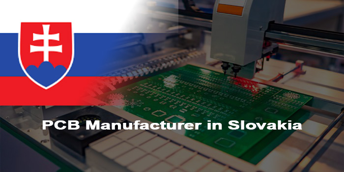
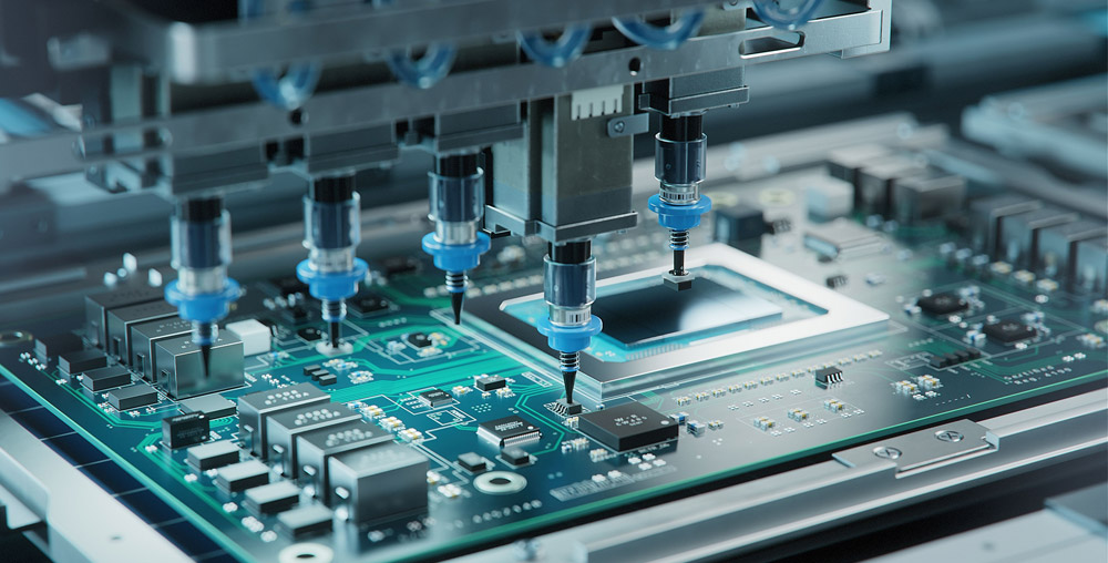
The PCB manufacturer in Slovakiaplays a crucial role in Europe’s electronic supply chain, offering diverse solutions for industrial, automotive and medical sectors. With mature industrial foundations and proximity to European markets, PCB manufacturer in Slovakiacontinues to expand their service scope, while facing fierce global competition. This blog covers top players, pain points, selection guides and future trends of Slovakia PCB, providing practical value for relevant businesses seeking reliable Slovakia PCB manufacturer.
Top 10 PCB Manufacturer in Slovakia
Company Name
Main Business
Core Advantages
Process Capabilities
Lead Time
EBest Circuit Co., Limited( Best Technology)
Multilayer/HDI/rigid-flex PCB
Global supply chain, EU compliance
1-32 layers, 3mil/3mil, blind vias
2-7 days
SQP International s.r.o
Multilayer/RF/turnkey PCB
30+ years, ISO 9001/14001, defense/medical
≤12 layers, <100µm lines, filled vias
2-5 days
UET PCB s.r.o
PCB fabrication/PCBA
99.99% yield, IATF16949/ISO13485
1-16 layers, Rogers/Isola, impedance
3-8 days
SVI Slovakia s.r.o
PCBA/box build/EMS
11,400㎡ facility, EU near-shoring
SMT/THT, 01005, vapor phase
4-10 days
GPV Electronics SK (H) s.r.o
PCBA/ODM/box build
Bratislava/Vienna logistics, lean
SMT/THT, burn-in, volume production
5-12 days
GPV Electronics SK (N) s.r.o
Prototyping/NPI/testing
17,000㎡ plant, 720 staff (since 1967)
High-volume SMT, system assembly
3-9 days
CRT Electronic s.r.o
Industrial PCBA
13+ years EU expertise, tailored
SMT/THT, small-batch, testing
3-8 days
Elcom s.r.o
Contract EMS/PCBA
R&D capability, cash register focus
Custom assembly, functional testing
4-10 days
Elpro s.r.o
SMT/THT assembly
In-house equipment, small-volume
Vacuum manipulators, reflow oven
3-7 days
SMT-Innovation s.r.o
SMT/assembly/equipment
20+ years EU experience, global
High-precision SMT, process optimization
2-8 days
Pain Points of PCB Manufacturer in Slovakia
Local Slovakia PCB factory lack ultra-fine line prototype capacity (below 3mil/3mil), relying on cross-border imports that extend lead times by 3-5 working days.
RoHS compliance pre-inspection for custom RF and high-Tg materials lengthens testing cycles, and small-batch prototype costs are 20-30% higher due to limited local scale.
Strict EU environmental regulations and high labor costs raise expenses for Slovakia PCB manufacturer, while mixed-brand equipment cuts efficiency by 10-15%.
Insufficient localized DFM support and specialized tools prolong design iterations for Slovakia PCB design, constrained by miniaturization and production limits.
Severe skilled labor shortage forces Slovakia PCB assembly plants to automate, yet 01005 component assembly still depends on limited skilled staff.
RoHS-compliant component supply disruptions and post-assembly testing add 1-2 working days to lead times, delaying production continuity.
How to Choose A Reliable PCB Manufacturer in Slovakia?
Verify Certification Qualifications: Prioritize manufacturers holding ISO 9001 (general quality), IATF 16949 (automotive-grade), and ISO 13485 (medical-grade) certifications—over 90% of leading Slovakia PCB factory possess these. Additionally, confirm UL certification and UL 94V0 flame retardant rating to ensure compliance.
Evaluate Process Capabilities: Beyond verifying 3mil/3mil line width accuracy and 12+ layer production capacity, check support for high-end materials like Rogers/Isola, blind/buried via technology, and ±1µm impedance control to meet precision requirements.
Control Yield Rate and Inspection: Optimize for manufacturers with a yield rate of ≥99.5%. For instance, UET PCB achieves a 99.99% yield rate through full-process quality inspection including AOI (Automatic Optical Inspection) and flying probe testing, ensuring mass production stability.
Consider Lead Time and Supply Chain: Confirm capacity for urgent prototypes (2-3 days) and mass production (5-7 days). Meanwhile, check inventory of core materials such as FR-4 and high-Tg substrates, as well as the dedicated processing mechanism for urgent orders.
Prefer One-Stop Services: Prioritize end-to-end services provided by a Slovakia PCB company, including DFM optimization, component sourcing, PCBA assembly, and after-sales functional testing to reduce collaboration costs.
Validate Supply Chain Stability: Understand partnerships with leading material suppliers (e.g., Isola, Rogers) to ensure supply of RoHS 3 compliant materials and avoid supply disruption risks.
Confirm Cost Transparency: Request a detailed quotation breakdown to clarify additional fees for testing, expediting, and customization, avoiding hidden costs that align with local production budget needs in Slovakia.
How to Evaluate the Lead Time of Slovakia PCB Manufacturer?
Order priority system: Confirm the manufacturer’s expedited service levels (e.g., 24/48-hour turnaround) for urgent orders and corresponding cost breakdowns to avoid hidden fees.
Raw material inventory: A reliable Slovakia PCB plant maintains ≥80% stock of core materials (FR-4, Rogers) to shorten material procurement cycles for standard orders.
Production schedule transparency: Require real-time order tracking tools to monitor progress and proactively alert for potential delays.
Equipment maintenance plans: Check scheduled maintenance protocols and target unplanned downtime rate (≤2% monthly) to minimize production disruptions.
Logistics partnerships: Prioritize manufacturers near Bratislava’s EU logistics hub, enabling next-day delivery to key European markets.
Batch size adaptability: Verify that lead time scales rationally, small batches should not incur excessive delays vs. mass production.
Quality control efficiency: Ensure in-line QA processes (AOI testing) to reduce rework, as post-production fixes can extend lead times by 1-2 days.
How to Evaluate the Production Capacity of Slovakia PCB Manufacturing Company?
Facility scale: Assess production area by tiers, small (≥2,000㎡) for batches, medium (≥8,000㎡) for stable mass output, and large (≥15,000㎡, e.g., GPV Electronics’ 17,000㎡ plant) for high volume. Top Slovakia PCB factory achieve ≥60% automation for core processes.
Machine precision: Confirm equipment supports fine-line fabrication (high-end 50µm, mainstream <100µm like SQP International), ±1µm LDI accuracy, and blind/buried via compatibility for Slovakia PCB.
Monthly output: A capable PCB manufacturer in Slovakia hits 30,000-50,000㎡/month (medium scale) and 50,000+㎡/month (large scale) to match local demand.
Quality control system: Require 100% AOI/X-ray testing for high-precision orders, target defect rate ≤0.3% (industry avg: 0.5-0.8%), and prioritize manufacturers like UET PCB with 99.99% yield rate.
Material sourcing network: Validate Isola/Rogers partnerships with 48-hour emergency replenishment, and ensure 100% RoHS 3 compliant suppliers.
Staff expertise: For medium facilities, require ≥50 skilled workers (80%+ IPC-A-610 certified) and ≥40 annual training hours per staff.
Certification scope: Confirm IPC Class 2/3 compliance (85% of top Slovakia PCB company meet this), plus IATF 16949 (automotive) and ISO 13485 (medical).
Future Challenges for Slovakia PCB Manufacturer
Rising labor costs in Slovakia, narrowing price gaps with Asian manufacturers.
Increased R&D investment pressure for advanced technologies (HDI, flexible PCB).
Stricter EU environmental regulations (RoHS 3 updates) raising production costs.
Shortage of high-tech talent for complex PCB manufacturing and design.
Supply chain volatility due to global component shortages and geopolitical risks.
Competition from neighboring EU countries (Austria, Germany) with mature PCB industries.
Demand for miniaturization pushing equipment upgrade costs for ultra-fine line production.
Shift to green manufacturing requiring eco-friendly materials and processes.
FAQs of Slovakia PCB Manufacturing
Q1: How to resolve microcracks in PCB substrates during production? A1: Microcracks stem from thermal stress and inferior materials. A professional PCB manufacturer in Slovakia uses high-grade substrates (Isola, Rogers) with stable thermal expansion and controls soldering temperature swings within ±5°C, plus thermal cycling (-40°C to 85°C) in prototype testing to eliminate defects.
Q2: Why do PCB prototypes have inconsistent impedance values, and how to fix it? A2: Inconsistency comes from imprecise line width and material variations. Slovakia PCB manufacturing adopts laser direct imaging (LDI) for ±1µm accuracy, pre-tests substrate batches, and provides DFM feedback to achieve 99.8% accuracy for impedance-controlled prototypes.
Q3: How to reduce delamination issues in multilayer PCB production? A3: Delamination is caused by moisture absorption and improper lamination pressure. An ISO 14001-certified Slovakia PCB plant conducts pre-baking (120°C for 4 hours), uses 35-40 psi vacuum lamination, and maintains humidity levels <45%.
Q4: What causes solder bridging in PCBA, and how to prevent it? A4: Solder bridging results from faulty stencil design and component placement. Automated SMT lines (10,500 components/hour) with optical centering, laser-cut stencils (0.1mm precision), and post-soldering AOI testing prevent this issue.
Q5: How to shorten lead time for custom high-Tg PCB orders in Slovakia? A5: Long lead times arise from material shortages and poor scheduling. A reliable PCB manufacturer in Slovakia stocks high-Tg materials (Tg 170°C+) and uses in-house production to offer 2-3 day prototype lead times for custom orders.
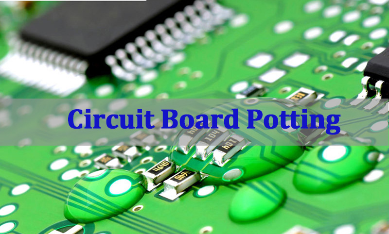
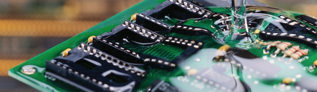
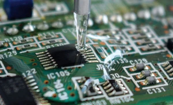
Circuit board potting is a critical encapsulation process in electronics manufacturing where a liquid compound is poured or dispensed over an assembled PCB (PCBA) and cured to form a solid, protective shell. This comprehensive guide explores the advanced materials, methods, and design considerations for potting printed circuit boards to ensure maximum reliability in demanding applications.
Ensuring long-term protection for PCB assemblies is challenging, and many products fail not because of design flaws, but due to inadequate circuit board potting strategies.
Premature Field Failures Moisture, vibration, and thermal cycling quickly degrade unprotected PCBs.
Material Selection Confusion Epoxy, silicone, or urethane—choosing the wrong compound risks performance and reliability.
Process-Induced Defects Air entrapment, voids, and cure stress compromise protection and component integrity.
No Path for Repair or Rework Poor potting decisions turn minor failures into full board scrap.
Added Weight and Cost Excessive potting weight on circuit boards impacts both BOM and product specs.
These challenges can be overcome by treating circuit board potting as an engineered PCBA process—not a material-only decision.
Engineered Reliability Potting systems are designed to match real thermal, mechanical, and environmental loads.
Scientific Material Selection The right epoxy resin circuit board potting compound is chosen based on data, not assumptions.
Controlled, Validated Processes Degassing, precision dispensing, and controlled curing eliminate voids and stress.
Design for Serviceability Where required, repairing potted circuit board assemblies remains feasible.
Optimized Weight and Cost Potting volume and geometry are engineered to protect—without unnecessary mass or expense.
At EBest Circuit (Best Technology), we specialize in transforming vulnerable electronic assemblies into ruggedized, reliable products. We are not just a PCBA manufacturer; we are your solution partner for advanced circuit board potting and encapsulation. Our engineers combine deep material science knowledge with state-of-the-art process controls to deliver potted assemblies that excel in the harshest environments. If you have any PCB inquiries, pls feel free to contact our engineering team at sales@bestpcbs.com.
What Is Circuit Board Potting in Printed Circuit Board Manufacturing?
Circuit board potting is a foundational protection process in electronics manufacturing. It involves completely enveloping a PCB assembly (PCBA) in a liquid resin that subsequently cures into a solid, monolithic block. This section defines the process, its objectives, and its place in the manufacturing workflow.
Core Objective: To provide a hermetic or near-hermic seal against environmental and operational threats.
Primary Threats Mitigated:
Environmental: Moisture, humidity, dust, debris, and corrosive gases.
Mechanical: Shock, vibration, and physical impact.
Electrical: Prevention of arcing, corona, and short circuits in high-voltage applications.
Chemical: Resistance to fuels, solvents, oils, and cleaning agents.
Process Placement: Typically a final manufacturing step after full PCBA testing, though sometimes done in stages for complex assemblies.
Unlike a surface-level conformal coat, potting fills all cavities and crevices, providing bulk, structural reinforcement and superior stress distribution. The result is a potted circuit board that behaves as a single, robust unit, significantly enhancing its operational lifespan in challenging conditions.
What Makes a Potted Circuit Board Different From an Unprotected PCBA?
Choosing between a potted board and an unprotected assembly is a fundamental design decision that directly impacts reliability, serviceability, and long-term performance in real-world environments.
Feature
Unprotected PCBA
Potted Circuit Board
Environmental Protection
None
Fully sealed
Mechanical Robustness
Low
High
Thermal Behavior
Air-dependent
Compound-influenced
Electrical Insulation
Limited
High dielectric strength
Repair & Rework
Easy
Very difficult
Weight & Volume
Minimal
Increased
An unprotected PCBA prioritizes accessibility, flexibility, and ease of debugging, making it suitable for controlled environments or products that require frequent servicing. In contrast, a potted circuit board fundamentally changes how the assembly behaves once deployed.
By encapsulating components in a solid compound, potting dramatically improves resistance to moisture, vibration, and electrical stress, while simultaneously limiting access for inspection, testing, or repair. Thermal performance also shifts from air-based cooling to conduction through the potting material, requiring careful compound selection and layout planning.
In short, potting a circuit board trades serviceability for survivability. The right choice depends on how harsh the operating environment is, how long the product must last without intervention, and whether field repair is a realistic requirement.
Why Do Engineers Choose Potting Circuit Boards for Harsh Operating Environments?
Engineers specify potting printed circuit boards when the application’s survival depends on maximum defense. It is the go-to solution for electronics that must operate reliably where other protections fail.
Outdoor & Automotive Electronics: Under-the-hood control units, LED drivers, and sensors face temperature extremes, condensation, and salt spray.
Industrial & Drivetrain Systems: Motor drives, power supplies, and controllers in factories withstand constant vibration, metal shavings, and coolant mists.
Marine & Submersible Devices: Navigation and sensing equipment requires a complete, high-pressure moisture barrier.
Aerospace & Defense Avionics: Systems must survive extreme G-forces, wide thermal cycling, and high-altitude conditions.
High-Voltage/Power Electronics: Potting prevents arcing, reduces corona discharge, and manages partial discharge, which is critical for longevity.
Consumer Durables: High-end tools, outdoor appliances, and wearables use potting for ruggedization and water resistance.
The choice for potting circuit boards is driven by a risk assessment: the consequences of field failure (cost, safety, reputation) far outweigh the added manufacturing complexity and cost of potting.
How Do You Select the Right Circuit Board Potting Material for Electronic Assemblies?
Selecting a circuit board potting compound is a multi-variable optimization problem. The ideal material balances protection with compatibility. The core question is rarely “will any epoxy work as circuit board potting?” but rather “which system provides the optimal property set?”
Define the Environmental Stressors: List all threats: operating temperature range, thermal cycling magnitude, chemical exposure, vibration spectrum, and required ingress protection (IP rating).
Understand Material Families:
Epoxies: High strength, good adhesion, excellent chemical resistance. Can be rigid, leading to component stress during thermal cycling.
Silicones: Extremely flexible, wide temperature range, good electrical properties. Lower mechanical strength and often higher cost.
Polyurethanes: A balance of flexibility, toughness, and good moisture resistance. Can be sensitive to moisture during curing.
Match Key Properties: Compare the candidate materials’ datasheets against your needs:
Coefficient of Thermal Expansion (CTE): Should match components/board to minimize stress.
Glass Transition Temperature (Tg): For epoxies, ensure operating temperature is below Tg or the compound becomes soft.
Modulus of Elasticity: A measure of stiffness (high modulus) vs. flexibility (low modulus).
Dielectric Strength & Constant: Critical for high-voltage or high-frequency boards.
Consider the Process: Assess pot life, mix ratio, viscosity, and cure schedule. A low-viscosity material flows better around dense components.
Evaluate Secondary Needs: Is optical clarity needed? Is UL94 V-0 flame retardancy required? Is repairing potted circuit board a future need (hinting at a reworkable silicone)?
For instance, a high-vibration automotive application might choose a flexible urethane, while a stable, high-heat power module might use a filled, thermally conductive epoxy.
When Is Epoxy Resin Circuit Board Potting the Preferred Encapsulation Method?
Epoxy resin circuit board potting is the workhorse of rigid encapsulation, chosen when the priority is creating a hard, fortress-like shell. It is not a universal solution but excels in specific scenarios.
When Maximum Mechanical Rigidity is Needed: For PCBs that are structural members or must resist high, constant mechanical loads.
For Superior Chemical Resistance: When exposed to aggressive solvents, fuels, or acids where other compounds might swell or degrade.
In High-Temperature, Static Environments: If the operating temperature is high but stable (minimal cycling), and is below the epoxy’s Tg. Epoxies can have a higher continuous use temperature than many urethanes.
For Excellent Adhesion to Diverse Substrates: Epoxy bonds tenaciously to metals, most plastics, and the PCB itself, preventing moisture ingress at interfaces.
When Cost-Effectiveness is Key: Epoxy systems are often more economical per volume than specialty silicones or urethanes.
For High Thermal Conductivity (When Filled): Loaded with ceramic or other fillers, epoxy resin circuit board potting compound can effectively move heat away from components, acting as a heatsink.
However, its rigidity is a double-edged sword. In applications with severe thermal cycling, the mismatch in CTE between the rigid epoxy and components can exert tremendous stress, potentially fracturing solder joints or the components themselves. This is a key decision point between epoxy and more flexible compounds.
How Does Potting a Circuit Board Impact Mechanical Strength and Thermal Behavior?
Potting a circuit board fundamentally alters its mechanical and thermal response. The compound doesn’t just add a layer; it couples all elements together, changing the system’s dynamics.
Mechanical Reinforcement:
Vibration Damping: The potting compound, especially flexible ones, absorbs vibrational energy, reducing the amplitude of oscillations transmitted to components. The damping effect can be modeled, but practically, it prevents solder fatigue.
Impact Resistance: The mass distributes a point impact load across the entire assembly, protecting fragile components. The compound’s toughness (ability to absorb energy) is critical here.
Stress on Components: A high-modulus (rigid) compound can transfer board flexure stresses directly to component leads. A low-modulus (flexible) compound allows for relative strain, reducing stress.
Thermal Management Redefinition:
From Convection to Conduction: Potting eliminates air flow. Heat must now be conducted through the compound to the outer casing. This makes the thermal conductivity (k) of the potting material a critical parameter.
The Thermal Path: The effectiveness depends on the compound’s ‘k’ value and the potting thickness on circuit boards. The thermal resistance (Rθ) of the potting layer is Rθ= thickness / (k * area). A thicker layer of a low-k material is a significant insulator.
System-Level Consideration: Design must ensure a clear conductive path from the heat-generating component, through the compound, to the enclosure or heatsink. Thermal interface materials (TIMs) or direct component bonding may be needed.
In summary, potting turns a collection of parts into a composite material. Its mechanical and thermal properties are now a weighted average of the PCB, components, and the potting compound itself.
What Design and Process Factors Matter When Using Circuit Board Potting Compound?
Successfully potting printed circuit boards requires forethought in both design and process. Ignoring these factors can lead to failure.
Design for Potting (DfP) Considerations:
Component Selection & Layout: Avoid components that can’t be potted (e.g., potentiometers, relays that need access). Orient tall components to facilitate compound flow. Create “flow channels” on the board.
Stress Relief: Use flexible glob-top or underfill for large BGAs or QFNs before global potting to mitigate CTE mismatch stress.
Venting and Filling: Design the enclosure with a fill port at the lowest point and a vent at the highest to ensure complete, bubble-free filling.
Potting Damns & Barriers: Use temporary or permanent dams to contain compound to specific areas if full-board potting isn’t required.
Material Compatibility: Verify that the compound is compatible with all component coatings, connectors, wire insulations, and the PCB solder mask.
Critical Process Controls:
Pre-Conditioning: Bake the assembly to remove moisture that could cause voids (“pop-corning”) during cure.
Mixing & Degassing: Precisely mix multi-part compounds and degas the mixture under vacuum to remove entrained air before dispensing.
Dispensing Technique: Use a controlled, slow pour or automated dispensing to allow the compound to flow and minimize air entrapment. Pour in a thin stream at the lowest point.
Cure Profile: Follow the manufacturer’s recommended time and temperature profile. Ramping the temperature too quickly can cause excessive exotherm and stress.
Inspection: Use ultrasonic scanning or X-ray to inspect for hidden voids or delamination in critical assemblies.
A well-designed board with a poorly controlled process (or vice-versa) will likely result in a defective potted circuit board.
Is Repairing Potted Circuit Board Possible in Production or Field Service?
The question of repairing potted circuit board assemblies is complex. The short answer is: it is often difficult, sometimes possible, and always expensive. Potting is designed to be permanent, and remove potting from circuit board is a destructive, high-risk procedure.
The Challenge of De-potting: The process to remove potted circuit board encapsulation is invasive. It often involves:
Mechanical Milling: Precise CNC milling to the component level, risking collateral damage.
Thermal Methods: Heating the entire assembly to the compound’s decomposition point, which can destroy all components.
Chemical Solvents: Using aggressive, heated solvents (e.g., nitric acid for epoxy) that can attack board laminates and components. This is a last-resort lab procedure, not a field service operation.
Designing for Serviceability:
Use of Reworkable Compounds: Some silicone potting circuit board applications or specialized urethanes are softer and can be cut and peeled away more easily, though it remains messy.
Modular/Compartmentalized Design: Pot only the sub-assembly that requires protection (e.g., the high-voltage section) and leave the control/logic section accessible in a separate compartment.
Connectors Over Direct Solder: Use connectors between potted and non-potted modules, allowing a faulty potted module to be replaced entirely.
In production, a failed board post-potting is almost always scrapped. In the field, the economics typically favor module replacement over attempting a de-potting circuit board and repair. Therefore, the decision to pot must be made with the understanding that the assembly is essentially rendered unserviceable.
To conclude, circuit board potting is a powerful transformative process that elevates a standard PCBA into a hardened, environmentally sealed device capable of surviving conditions that would defeat lesser protections. This guide has detailed the critical considerations, from material science and mechanical impacts to design and process controls, that define successful potting.
Mastering advanced potting is not about simply filling a box with resin; it is the strategic integration of material properties, mechanical design, and precise manufacturing to solve reliability challenges. It moves beyond the question of “how to pot a circuit board” to “how to design a system where potting ensures flawless, long-term operation.”
At EBEST CIRCUIT (Best Technology), this strategic mastery is applied directly to every customer project. EBEST CIRCUIT (Best Technology) analyzes stress profiles, selects the optimal compound—whether a rugged epoxy resin circuit board potting system or a flexible silicone—and applies controlled, repeatable processes to ensure each potted circuit board meets defined reliability targets. For a consultation on your next PCB or PCBA project, pls feel free to contact us at sales@bestpcbs.com.
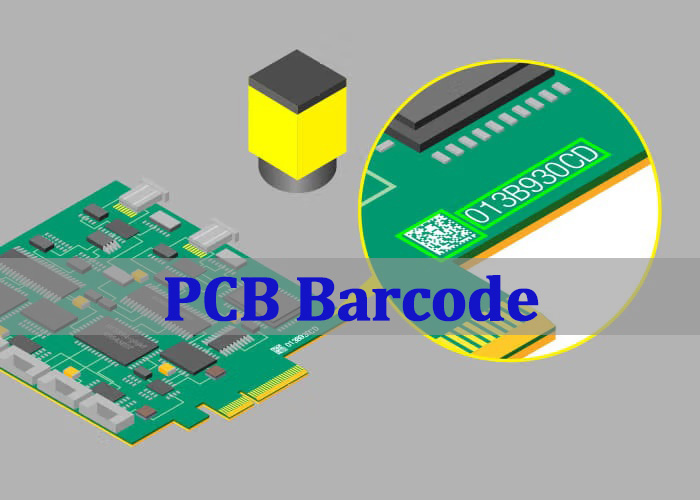
PCB barcode is a machine-readable identifier permanently marked on a bare circuit board. This guide delves into everything from the fundamentals of PCB barcode labels to advanced system integration for full traceability.
Without a structured PCB barcode system, manufacturers face hidden risks that directly impact quality, efficiency, and cost.
No Traceability: Failed boards cannot be reliably linked to PCB lots, materials, or processes.
Human Errors: Manual serial number entry causes data inaccuracies and quality record gaps.
MES Disconnection: Board IDs exist but are not tied to MES or production data.
Slow Identification: Manual checks delay assembly, testing, and inspection steps.
Higher Recall Costs: Lack of lot-level data forces wide, expensive recalls.
How a Professional PCB Manufacturer Solves These Challenges?
End-to-End Tracking: Permanent barcode laser marking links each board to its full history.
Error-Free Data Capture: Machine-readable codes eliminate manual input mistakes.
MES-Ready Barcodes: Formats align with MES and ERP systems for seamless data flow.
Faster Production: Automated scanning accelerates SMT, testing, and programming.
A professional PCB manufacturer embeds PCB barcode capabilities directly into fabrication and production workflows to enable reliable, end-to-end traceability. EBest Circuit (Best Technology) is a professional PCB and PCBA manufacturer specializing in advanced identification and traceability solutions. We provide a full range of PCB solutions, including FR4 PCBs, flexible and rigid-flex circuits, metal core and ceramic PCBs, along with PCB layout, PCBA and complete box-build services. For traceable, reliable circuit boards, pls feel free to contact us at sales@bestpcbs.com.
What Is a PCB Barcode?
A PCB barcode is a unique, machine-readable data carrier that is directly marked on the surface of a printed circuit board (PCB). It serves as the board’s permanent “digital license plate,” enabling automated identification and data collection throughout its lifecycle—from fabrication and component assembly (PCBA) to field service.
Core Functions of a PCB Barcode:
Unique Identification: Distinguishes one board from millions of others.
Data Carrier: Stores essential information in a compact format.
Automation Enabler: Allows machines like a barcode scanner PCB reader to instantly identify the board.
Traceability Anchor: Links the physical board to its digital record in databases.
In essence, it is the foundational element for Advanced PCB Barcode Integration for Traceable PCB and PCBA, turning a passive component into a smart, trackable asset.
What Information Is Stored in a PCB Barcode?
The barcode itself typically contains a unique identifier, like a serial number. This key is then used to access a comprehensive digital record stored in a database (e.g., MES, ERP). The linked data can include:
Data Category
Examples
Manufacturing Data
Lot number, fabricator ID, fabrication date, panel ID.
Test results, inspection history, certifications (UL, ISO).
Supply Chain Data
Supplier info, PO number, delivery batch.
In summary, the barcode on PCB is a compact key that unlocks a vast, detailed history of the board, which is crucial for quality control and traceability.
What Is the Difference: PCB Barcode vs Serial Number vs QR Code
This comparison highlights how common identifiers on PCB boards differ in purpose, data capacity, and traceability value.
Quick Comparison of PCB Identification Methods
Feature
PCB Serial Number
Linear (1D) Barcode
QR Code / PCB 2D Barcode
Format
Human-readable text
Parallel lines (1D)
Square matrix (2D)
Data Capacity
Low
Low–Moderate
High
Read Method
Visual / manual
Scanner
Scanner / vision
Space Required
Moderate
Long, linear
Compact
Durability
Human-dependent
Sensitive to damage
High error correction
Traceability Use
Reference only
ID automation
Full traceability
To conclude, a PCB serial number is intended for human reference, a linear PCB barcode automates reading that identifier, while a PCB QR code or PCB 2D barcode supports high-density data storage and is the preferred choice for modern PCB and PCBA traceability systems.
What Is the Difference: PCB 2D Barcode vs Linear Barcode on PCB Boards
Choosing the right mark impacts your traceability system’s effectiveness.
Linear Barcode (e.g., Code 128, Codabar):
Structure: Encodes data in the varying widths of parallel lines and spaces.
Data: Can only store a string of numbers/letters (an ID).
Scanning: Requires precise alignment with a laser scanner.
Space: Needs a relatively long, rectangular space.
Durability: A single damaged line can render it unreadable.
A Codabar barcode example is sometimes used in legacy library or logistics systems.
2D Barcode (e.g., Data Matrix, QR Code):
Structure: Encodes data in a grid of black/white squares or dots.
Data: Can store hundreds of characters, including text, numbers, and URLs.
Scanning: Can be read from any angle (omnidirectional) by an imager scanner.
Space: Stores vast information in a very small area (as small as 2×2 mm).
Durability: Built-in error correction allows it to be read even if partially damaged.
In brief, for modern PCB barcode laser marking, 2D barcodes are overwhelmingly preferred due to their superior data capacity, small size, and reading reliability.
How Do I Identify a PCB Board?
Identifying a PCB board involves locating and interpreting its permanent identifiers.
Visual Inspection: Look for a string of text (serial/part number) or a barcode on PCB.
Locate Markings: These are often found in a corner, near the edge, or in an unused area of the solder mask.
Use a Scanner: Employ a handheld barcode scanner or fixed barcode scanner PCB reader to automatically decode the information.
Consult Documentation: Cross-reference the found number with assembly drawings, bills of materials (BOM), or manufacturer data.
What Is the PCB Identification Number?
The PCB identification number is the structured code used to uniquely identify a PCB design or an individual board throughout manufacturing, assembly, and quality control. In professional PCB and PCBA production, it forms the backbone of traceability and compliance.
In practice, the PCB identification number is implemented in two complementary forms:
Part Number The part number defines the PCB design itself, including layout, material set, layer stack-up, and revision level (for example, BRD-100A-REV2). All boards produced to the same design share this identifier, making it the reference point for engineering control and document management.
Serial Number (UID) The serial number is a unique identifier assigned to each individual PCB or PCBA (for example, SN-2049000157). This UID is the foundation of unit-level traceability and is typically encoded into the PCB barcode—either via barcode labels or permanent laser marking—so every board can be tracked independently.
At EBest Circuit (Best Technology), PCB identification numbers are not treated as static markings, but as active data keys within a fully integrated manufacturing and quality system.
MES-Driven Traceability Each PCB serial number is digitally bound to our MES, linking fabrication data, process parameters, inspection records, and PCBA assembly history into a single traceable record.
Compliance with ISO13485 and IATF16949 Our identification and barcode practices are designed to meet the traceability requirements of medical and automotive standards, supporting audit-ready documentation, lot control, and recall containment.
Seamless PCB to PCBA Data Continuity The same PCB identification number follows the board from bare PCB fabrication through SMT, testing, and final assembly, eliminating data breaks between processes.
Laser Marking and Barcode Integration We apply durable PCB barcode laser marking solutions that ensure long-term readability through reflow, cleaning, and handling, while remaining fully compatible with automated inspection and MES scanning.
In essence, when a quality issue occurs, a properly implemented PCB identification number allows engineers to trace a failure back to a specific board, batch, material set, and process step, instead of isolating entire lots. This level of precision reduces investigation time, limits recall scope, and protects both product reliability and brand reputation.
Where Can I Get My PCB Number?
Your PCB number is assigned and applied by your PCB manufacturer.
Part Number: You (the designer/OEM) provide this based on your internal numbering system.
Serial Number (UID): This can be:
Sequentially Assigned by the Manufacturer: The PCB barcode scanner PCB board manufacturer generates and marks it.
Defined by Customer: You provide a list of UIDs for the manufacturer to apply.
Rule-Based Generation: Created algorithmically from lot, date, and panel data.
Ensure your China barcode scanner PCB board suppliers or any manufacturer clearly communicates their numbering protocol.
PCB Barcode Laser Marking vs Label PCB Printing Methods
Choosing the right PCB barcode application method directly affects durability, traceability, and long-term reliability.
Feature
Laser Marking
Label Printing
Application
Direct marking
Adhesive label
Process
Etched on surface
Printed & attached
Durability
Permanent
Limited
Heat/Chemical Resistance
High
Low–Moderate
Mark Size & Detail
Very high
Moderate
Cost Structure
Low per unit
Ongoing materials
Typical Use
Production PCBs
Prototypes
In fact, PCB barcode laser marking creates permanent, high-precision identifiers that survive soldering, cleaning, and long-term use, making it the preferred method for traceable PCB and PCBA manufacturing. Label PCB printing remains suitable for prototypes, low-stress applications, or cases where direct marking is not feasible.
How PCB Barcodes Are Scanned and Managed in MES Systems?
This is where Advanced PCB Barcode Integration delivers value. The process creates a closed-loop data system.
Marking: A unique 2D barcode PCB is laser-marked during fabrication.
SMT & Assembly: At each station (paste, pick-place, reflow), a barcode scanner reads the board. The MES logs which components from which reels were placed on this specific boardat this specific time.
Testing & Programming: The board ID automatically pulls up the correct test profile or firmware program. Results (pass/fail, values) are saved back to the board’s record.
Data Hub (MES): The MES acts as the central brain, storing the complete history linked to the barcode key.
Traceability & Analytics: For any field return, scanning the barcode reveals its full genealogy and process history, enabling instant root cause analysis.
Why PCB Barcode Matters for Traceability and Quality Control?
Implementing a PCB barcode system is a strategic investment, not just a procedural step.
Full-Unit Traceability: Isolate failures to a specific batch, shift, or component reel.
Process Control: Monitor yield in real-time and identify bottleneck stations.
Automated Data Capture: Eliminate manual logs, ensuring data integrity and freeing operator time.
Compliance & Reporting: Easily generate audit trails for industry standards (IATF 16949, ISO 13485).
Overall, PCB barcode is the cornerstone of modern electronics traceability, transforming passive boards into intelligent, data-rich assets. This guide has explored its technology, application, and critical role in Advanced PCB Barcode Integration for Traceable PCB and PCBA.
EBest Circuit (Best Technology) understands that quality and traceability are indispensable in the medical, industrial control, and IoT industries. To ensure this, our PCB production lines utilize a comprehensive MES system, guaranteeing full traceability for every single PCB and PCBA we manufacture. Our facility holds ISO 13485 and AS9100D certifications, underscoring our commitment to these demanding sectors. We have collaborated with engineers in the medical device and aerospace fields for nearly two decades, with production records for some projects preserved for up to 10 or even 15 years. If you have an upcoming PCB or PCBA project, please send your Gerber files, BOM, and board requirements to sales@bestpcbs.com for a quote and a complimentary DFM analysis.
FAQs
What Are PCB Barcode Labels?
PCB barcode labels are adhesive tags printed with a barcode (often a PCB QR code or 2D symbol) and the human-readable number. They are affixed to the board as an alternative to direct laser marking. While useful for prototypes or certain applications, they are less durable than direct marks for full traceability through PCBA processes.
What Is a PCB Number?
A PCB number broadly refers to any identifying code on a circuit board. Most critically, it is the Unique Identifier (UID) or serial number that is unique to each single board. This number, often encoded in a barcode on PCB, is the primary key for accessing the board’s digital history in a traceability system, answering the fundamental question, “What is a printed circuit board (pcb)’s specific history?“
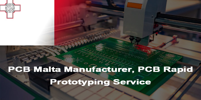
Looking forPCB Malta manufacturer? This blog covers main pain points of Malta PCB manufacturer and our solutions to these points.
Malta’s electronics industry relies heavily on reliablePCB Malta manufacturerand high-quality PCB manufacturing Malta services. As demand for precision electronics grows locally, sourcing a trustworthy PCB manufacturer in Malta becomes crucial for seamless production workflows. This guide covers the top local players, core industry pain points, and how leading local manufacturers deliver tailored solutions aligned with Malta’s unique production needs and EU compliance standards.
Top PCB Malta Manufacturer in 2026
Company Name
Main Business
Core Advantages
Process Capability
Lead Time
EBest Circuit Co., Limited
PCB prototyping/mass production/HDI boards
19-year experience, 24h urgent prototyping
40-layer HDI, 0.1mm line width
24hrs-15 days
Electronics Malta Group
Consumer electronics PCBs
Cost-effective, RoHS compliance
16-layer, flexible substrate
4-18 days
Malta Electronics Solutions OÜ
Medical PCB
ISO13485, cleanroom
24-layer, biocompatible
12-22 days
TechPrint Malta Ltd
Single/double-layer PCBs
Fast small-batch
Standard finishes
2-10 days
HDI Malta Electronics OÜ
HDI/telecom PCBs
REACH compliance
30-layer HDI, PTFE
14-25 days
GreenCircuit Malta Ltd
Eco-friendly PCBs
Waste recycling
Halogen-free
9-18 days
Pain Points of PCB Malta Manufacturer
Urgent PCB prototyping demands cannot be met, with standard lead times exceeding 7 days, delaying project progress.
Design flaws are detected late in production, leading to rework, increased costs, and extended timelines.
Inconsistent product quality across batches, with issues like board warpage and poor solderability affecting usability.
High material costs for special substrates (e.g., high-frequency, medical-grade) without cost-saving alternatives.
Limited process capability for complex designs, such as HDI boards with blind/buried holes and fine line widths.
Lack of professional support for PCB printing Malta, resulting in unclear silk-screen and poor mark visibility.
Unreliable delivery schedules, with frequent delays due to inefficient production planning.
Insufficient testing processes, leading to hidden electrical faults in finished PCBs.
Our PCB Solutions to These Pain Points
Pre-Production Design Support: Provide free DFM analysis to identify potential design flaws early, avoiding rework. Our team optimizes designs for manufacturability while maintaining performance, addressing late-stage design issue pain points.
Flexible Prototyping Service: Offer 24-hour urgent PCB prototyping and 3-7 day standard prototyping, fully meeting tight project schedules. Advanced automated lines ensure fast sampling without compromising quality.
Cost-Optimization Solutions: Cooperate with top substrate suppliers to provide cost-effective alternatives for special materials. Customize cost-sensitive plans based on production volume, reducing material cost burdens.
Advanced Process Capability: Master HDI, blind/buried hole, and fine line processing technologies to handle complex designs. Professional PCB printing Malta equipment ensures clear silk-screen and durable marks.
Strict Quality Control: Implement full inspection for mass production, including automated optical inspection (AOI), electrical testing, and board warpage detection. Achieve consistent quality across batches with a 99.8% pass rate.
MES System Full-Process Traceability: MES enables real-time production monitoring and full-process traceability, covering raw material intake, processing, testing, and delivery. Clients access real-time progress to avoid delivery doubts. MES-driven smart planning ensures 99.2% on-time delivery.
Post-Delivery Support: Offer technical consultation and fault analysis for finished products. Provide rework solutions for any quality issues, ensuring worry-free use of PCB Malta products.
Why Choose EBest(Best Technology) asPCB Malta manufacturer?
24-Hour Urgent Prototyping: Unique rapid production lines complete PCB prototyping within 24 hours, the fastest in the Malta market for urgent orders.
Competitive Pricing: 19 years of industry experience enables optimized supply chains, offering 10-15% lower costs than peers for the same quality PCB manufacturing Malta.
Cost-Sensitive Solutions: Customize material selection and process plans based on project needs, reducing unnecessary expenses without sacrificing performance.
High On-Time Delivery Rate: 99.2% of orders are delivered on schedule, supported by smart production scheduling and sufficient inventory.
Strict Quality Control: Mass production adopts 100% full inspection, with 8-stage quality checks from material incoming to finished product delivery, ensuring stable quality.
Rich Industry Experience: 19 years of serving global clients helps optimize designs and processes, reducing overall project costs by 8-12%.
Free DFM Analysis: Professional team provides detailed design optimization suggestions before production, eliminating rework risks.
Comprehensive Certifications: Hold ISO9001:2015, ISO13485:2016, REACH, RoHS, and IATF16949 certifications, meeting diverse industry requirements.
One-Stop Service: Integrate PCB printing Malta, prototyping, mass production, and testing, simplifying procurement processes for clients.
Localized Support: Set up a local service team in Malta to provide fast technical consultation and after-sales support, responding within 2 hours.
Our PCB Rapid Prototyping Service
EBest’s PCB rapid prototyping service prioritizes speed to meet our clients’ urgent project needs. With four dedicated express production lines, we achieve a 99.5% on-time delivery rate for 24-hour expedited prototyping, 50% faster than the average in the Maltese market. Even for complex PCB designs, from single-layer boards to 40-layer HDI prototypes, we maintain the same rapid turnaround time, thanks to the strong support of high-precision exposure machines and automated processing equipment. Each prototype undergoes 18 rigorous quality checks (including AOI optical inspection and impedance testing), ensuring a 99.8% yield rate, consistent with mass production standards. Whether you face last-minute design adjustments or urgent project deadlines, our expedited service delivers reliable Maltese PCB prototypes on time, helping you shorten development cycles and gain a competitive edge in the market.
Background: A Malta industrial automation equipment firm required high-reliability PCB Malta for its new control system, targeting harsh industrial environments with strict temperature stability and anti-interference for 2GHz high-frequency signals.
Requirements: 16-layer HDI PCB, operating temperature -40℃ to 85℃ (1,000-hour thermal cycle resistance), impedance control ±5% for 2GHz signals, prototype lead time ≤10 days, mass production (5,000 units) ≤20 days.
Difficulties: Impedance stability control for 2GHz high-frequency signals (industry standard Df ≤0.01), 16-layer lamination risk of board warpage exceeding IPS standard (≤0.75%), and compressed lead time 30% shorter than market average.
Solutions: Adopted high-temperature FR-4 substrate (Tg 180℃) and optimized lamination parameters (180℃/350PSI) to control warpage ≤0.5%; Used precision etching (±0.02mm tolerance) with 3 rounds of impedance calibration tests; Allocated dedicated expedited lines via MES scheduling for time guarantee.
Results: Prototypes delivered in 7 days, 5,000 mass-produced units in 18 days (10% faster than required). All passed 1,000-hour thermal cycle and 2GHz anti-interference tests, with 100% pass rate and warpage ≤0.4%. The client launched on schedule, and 60% of their subsequent industrial control projects designate us as the exclusive PCB manufacturer in Malta.
FAQs of PCB Manufacturing Malta
Q1: How to avoid board warpage in multi-layer PCB production? A1: We optimize lamination parameters (temperature, pressure, holding time) and adopt symmetric layer design to balance stress. Post-production mechanical correction and thermal aging treatment further reduce warpage. Contact us for customized warpage control solutions for your PCB Malta project.
Q2: Can design flaws be detected before PCB prototyping? A2: Yes. We provide free DFM analysis to check for design issues like unreasonable line width/space, improper hole size, and silk-screen conflicts. This reduces rework rates by over 90%. Reach out for pre-production design validation.
Q3: What surface treatment is best for PCB printing Malta in humid environments? A3: Immersion gold or OSP surface treatment is recommended for humid conditions, as they offer excellent corrosion resistance. We can tailor surface treatment plans based on your application environment. Inquiry now for personalized suggestions.
Q4: How to reduce costs for small-batch PCB manufacture Malta? A4: We offer shared mold services and optimize material cutting to reduce waste. Our cost-sensitive solutions can lower small-batch production costs by 10-15%. Contact us to get a cost-saving quote.
Q5: What tests are conducted for medical PCB products? A5: Medical PCBs undergo electrical testing, insulation resistance testing, biocompatibility testing, and temperature cycle testing, complying with ISO13485 standards. We provide full test reports for each batch. Inquiry for medical-grade PCB prototyping and production services.
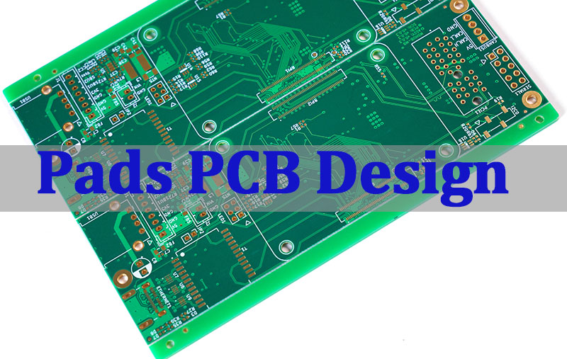
Effective Pads PCB design is a cornerstone of creating reliable, high-performance printed circuit boards (PCBs). Pads serve as the critical connection points between components and the conductive traces of the board. This guide explores advanced concepts, materials, types, and design rules to optimize your PCB pad design for manufacturing (DFM) and long-term reliability.
Does poor pad design constantly undermine your PCB’s reliability and manufacturability?
Frequent Solder Defects: Incorrect pad size or shape leads to tombstoning, bridging, or poor joints.
Thermal Management Failure: Inefficient thermal pad design causes component overheating and reduced lifespan.
Signal Integrity Issues: Poor pad-to-trace transitions create impedance discontinuities, degrading signal quality.
Manufacturing Headaches: Pads incompatible with soldering processes cause low assembly yield and rework.
Long-Term Reliability Risks: Weak pad connections fatigue and crack under thermal or mechanical stress.
Addressing these requires systematic design strategies focused on pad optimization.
Precision Pad Geometry: Design pads per IPC standards and datasheets to ensure perfect solder fillets and joint strength.
Optimized Thermal Management: Use via-in-pad with thermal simulation for effective heat dissipation from power components.
Signal Integrity First: Apply controlled impedance design and smooth transitions at pads to maintain signal quality.
DFM-Driven Design: Adhere to strict solder mask and stencil guidelines for flawless SMT assembly.
Robustness Engineering: Reinforce connections with teardrops and robust pad structures verified by stress analysis.
EBest Circuit (Best Technology) offers a comprehensive range of solutions, including rigid PCBs, flexible circuits, rigid-flex circuits, metal-core PCBs, ceramic PCBs, PCB layout, and box-build assembly. Founded in 2006, we have specialized in one-stop PCB and PCBA services, covering PCB design, component sourcing, rapid prototyping, volume production, PCB assembly, and full box-build solutions. Our engineering and sales teams are professionally trained, with many members bringing over 10 years of hands-on project experience supporting global customers. We are certified to ISO 13485, AS9100D, and IATF 16949, and our production lines are integrated with an MES system to ensure traceability and process control. Our core focus markets include medical devices, aerospace, industrial control, and IoT applications, where reliability and compliance are critical. For factory audits or partnership inquiries, please contact us at sales@bestpcbs.com.
What Is Pads PCB Design?
Pads PCB design refers to the strategic planning, sizing, shaping, and placement of the conductive contact areas on a PCB where components are soldered. These circuit board pads are the fundamental interface for surface-mount (SMD) and through-hole components. The primary goal is to ensure a robust mechanical and electrical connection that can withstand assembly processes, thermal cycling, and operational stresses.
What Are PCB Pads Made Of?
PCB pads are fabricated from the same copper foil layer that forms the board’s traces. The process involves:
Copper Foil: Typically Electrodeposited (ED) or Rolled Annealed (RA) copper, laminated onto the substrate.
Surface Finish: A thin coating applied over the bare copper to prevent oxidation and enhance solderability. Common finishes include:
HASL (Hot Air Solder Leveling): A traditional, cost-effective tin-lead or lead-free coating.
ENIG (Electroless Nickel Immersion Gold): Provides a flat surface, excellent for fine-pitch components and gold wire bonding.
OSP (Organic Solderability Preservative): A thin organic layer that protects copper until soldering.
Immersion Silver/Tin: Offers good solderability and a relatively flat surface.
Solder Mask: The polymer layer that covers most of the PCB but opens up at the pad locations to define the solderable area. Its proper alignment is critical.
What Are Design Pads For?
Pads serve multiple essential functions:
Electrical Connection: Provide the conductive path for signals and power between the component and the PCB traces.
Mechanical Anchor: Physically secure the component to the board.
Thermal Path: Act as a channel to transfer heat from the component to the PCB planes or heatsinks, especially crucial for thermal pad PCB design.
Soldering Interface: Define the area where solder forms the joint.
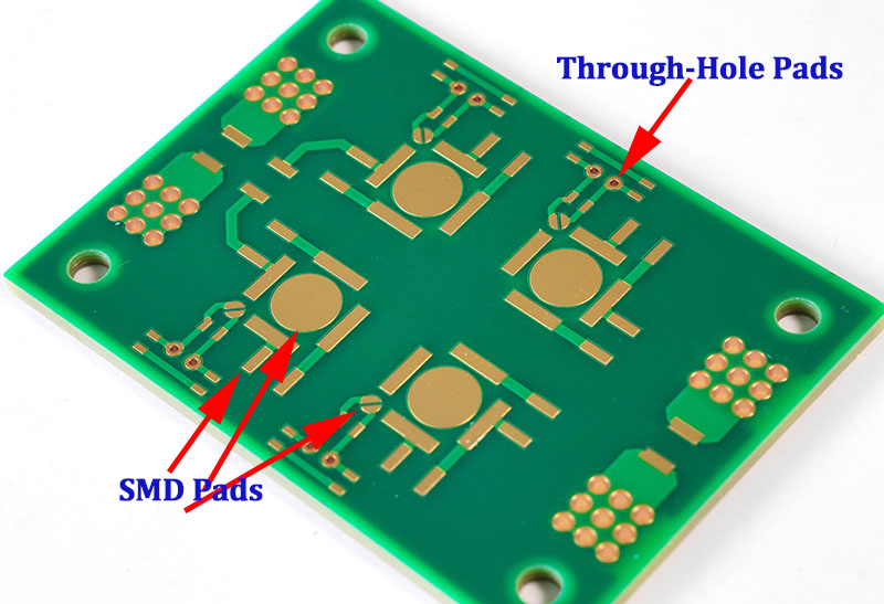
Types of PCB Pads and Their Applications
In PCB design, pads are more than simple solder points. Different pad types serve distinct electrical, mechanical, thermal, and manufacturing purposes. Understanding these differences helps engineers make faster, more reliable design decisions—especially when balancing assembly yield, testability, and long-term reliability.
While the table provides a quick reference, each pad type introduces specific design trade-offs that deserve attention during layout:
SMD Pads: Pad geometry directly affects solder wetting, tombstoning risk, and placement accuracy. IPC footprint standards are often the starting point, but manufacturing capability must be considered.
Through-Hole Pads: Hole diameter, annular ring width, and plating thickness determine mechanical strength and solder fill quality, especially in multi-layer boards.
Thermal Pads: These pads strongly influence junction temperature and solder voiding behavior. Via patterns, paste coverage ratio, and reflow profiles must be coordinated, making thermal pad PCB design a cross-disciplinary task.
Test Pads: Test accessibility is often overlooked until late in the project. Early planning improves coverage without increasing board size.
Fiducial Pads: In PCB manufacturing, fiducial pads refer to optical fiducials realized as solid copper pads. Though electrically inactive, fiducials are critical for placement accuracy in high-density SMT assembly.
Solder Bridge Pads: These enable low-cost configuration changes but require careful spacing to avoid unintended shorts during reflow.
In a nutshell, different PCB pad types exist because no single pad design fits every electrical, thermal, or manufacturing requirement. A well-chosen pad strategy improves assembly yield, testability, thermal performance, and overall product reliability.
What Is Anti Pad in PCB Design?
An anti-pad is a clearance hole in an internal copper plane (power or ground) that electrically isolates a via or plated through-hole barrel from that plane. It prevents an unintended short circuit. The size of the anti-pad is a critical part of the PCB pad stack design and must be large enough to ensure proper insulation while maintaining plane integrity.
Difference Between Holes and Pads in PCB Design
This is a fundamental distinction in PCB pad hole design:
Hole: A physical drilled cavity in the PCB. Its primary purposes are:
To accommodate the lead of a through-hole component.
To form the barrel of a via (for layer-to-layer connection).
Pad: The copper land area that surrounds and connects to the hole. Its functions are:
For Through-Hole Components: Provides the annular ring for soldering the lead and creating a reliable connection.
For Vias: Can be a “tented” SMD pad on the surface or an internal connection point.
In short, the hole is the void; the pad is the conductive material around it that makes the connection possible.
Important Considerations for Pads PCB Design
Adhering to PCB pad design guidelines is essential for manufacturability and reliability.
Pad Size & Shape (Land Pattern): Follow IPC-7351 standards. Pads must be large enough for a reliable solder fillet but not so large as to cause bridging or tombstoning.
Solder Mask Definition: The solder mask opening should be slightly larger than the copper pad (typically 0.05-0.1mm per side) to prevent misalignment from exposing the trace.
Silkscreen Clearance: Silkscreen PCB design guidelines mandate that ink must never cover a pad. Maintain a minimum clearance (e.g., 0.2mm) to avoid contamination.
Copper-to-Edge Clearance: Pads, especially for connectors, must be set back sufficiently from the board outline to prevent shorting during routing.
Trace Connection: Use teardrops where PCB design trace between pads or traces connect to small pads/vias to strengthen the joint and prevent cracking.
Thermal Relief Pads: Use for connections to large copper planes (like ground) to prevent heat sinking, which makes soldering difficult.
Thermal Pad Design and Solder Voiding
Thermal pad PCB design for components like QFNs is critical. A central pad with a grid of small vias (“via-in-pad”) is used for heat dissipation. However, this can lead to solder voiding as gases escape during reflow. Mitigation strategies include:
Via-in-Pad Design: Use small diameter vias (e.g., 0.2mm) and ensure they are filled and capped (with epoxy or copper) to prevent solder wicking into the via and creating voids.
Solder Paste Stenciling: Use a segmented stencil opening (grid of small apertures) over the thermal pad instead of one large opening to allow gases to escape.
Optimized Reflow Profile: A slower temperature ramp can help gases escape before the solder seals the area.
Via-in-Pad Techniques and Design Trade-Offs
PCB design via in pad places vias directly in the SMD pad, offering significant benefits but requiring careful management.
Advantages:
Space Savings: Eliminates the need to route traces away from the pad to access a via.
Improved Electrical Performance: Provides the shortest possible path for high-speed or power signals, reducing inductance.
Enhanced Thermal Conductivity: Critical for thermal modeling and design optimization of PCB vias and pads under BGAs and QFNs.
Trade-Offs and Solutions:
Solder Wicking/Voiding: Solder can flow down the via barrel, starving the joint. Solution: Specify filled and plated-over (capped) vias.
Increased Cost: Via filling and capping adds process steps and cost.
Assembly Complexity: May require sequential lamination or specialized processes.
A related but distinct practice is PCB design vias on pads for through-hole components, where vias are placed adjacent to the component hole’s pad to route signals to other layers, which is generally more straightforward.
FAQs
Q: What Is the Difference Between a Pad and a Via?
A: A pad is primarily designed to make a connection to a component lead. A via is a plated through-hole designed solely to provide an electrical connection between different layers of the PCB. A via can be placed within a pad (via-in-pad) or connected to it by a short trace.
Q: What Is the Difference Between a Pad and a Lead?
A: The pad is the copper feature on the PCB. The lead (or pin) is the metallic terminal of the electronic component that is soldered to the pad.
Q: What Are the Key Elements of Pad Design?
A: The key elements are defined in the PCB pad stack design and include:
Copper Layer Geometry: Size, shape, and orientation of the pad on each relevant layer.
Solder Mask Opening: Size and alignment relative to the copper.
Paste Mask Layer (for SMD): Defines the stencil aperture for solder paste.
Drill Information (for through-hole): Hole size and location.
Anti-pad Size (for planes): Clearance in internal copper layers. By mastering these elements, you ensure your PCB design pads form the foundation of a robust and reliable circuit assembly.
Q: Are Fiducial Pads the Same as PCB Fiducial Markers?
A: Yes. In PCB engineering and SMT assembly, fiducial pads and PCB fiducial markers refer to the same functional feature. Both describe exposed copper reference points used by pick-and-place machines, AOI systems, and other automated assembly equipment to accurately locate and align the PCB during component placement.
The term PCB fiducial markers is the industry-standard expression commonly used in SMT process documentation and equipment manuals, while fiducial pads emphasizes the physical pad structure on the PCB itself. In practice, the two terms are interchangeable, and the difference is mainly one of wording rather than function.
Latvia’s PCB manufacturing sector boasts reliable production capabilities and strict quality control, making PCB Latvia manufacturer a trusted choice for regional electronic projects. With a manufacturing capacity utilization rate of 75.1% in late 2025, the industry balances precision and efficiency to meet diverse project needs. Whether for prototyping or mass production, PCB Latvia manufacturer integrates advanced technologies and European standards, solidifying its position in the Baltic electronic supply chain. This guide covers top suppliers, quality benchmarks, pain points, and selection strategies to support informed decisions for Latvia PCB projects.
Top 10 PCB Manufacturer in Latvia
Company Name
Main Business
Core Advantages
Process Capability
Lead Time
EBest Circuit Co., Limited
Metal core PCB design/fabrication
18-year experience, ISO certified, 30,000㎡ factory
Quality Certifications for PCB Latvia Manufacturer
ISO 9001:2015: A baseline mandatory certification for Latvia PCB company operations. It establishes a standardized quality management system, covering production processes, raw material inspection, and after-sales service to ensure consistent product quality.
RoHS Certification: An EU mandatory environmental certification for electronic products. It restricts the use of 10 hazardous substances (e.g., lead, mercury) in Latvia PCB manufacturing, with lead content limited to ≤0.1% to comply with EU environmental directives.
REACH Certification: Another EU mandatory environmental certification. It regulates the registration, evaluation, authorization, and restriction of chemicals used in Latvia PCB plant production, ensuring no harmful substances pose risks to human health and the environment.
CE Certification: A mandatory safety certification for products entering the EU market. All PCB Latvia products must obtain CE marking, proving compliance with EU technical directives including EMC and safety requirements.
ISO 13485: Mandatory for Latvia PCB manufacturer serving the medical industry. It specifies quality management system requirements for medical device-related PCBs, ensuring compliance with medical industry safety and effectiveness standards.
IATF 16949: Essential for Latvia PCB factory supplying the automotive sector. This certification aligns with global automotive industry quality standards, covering production control, traceability, and defect prevention for automotive-grade PCBs.
IPC-A-610: A mandatory assembly quality standard. It defines acceptability criteria for Latvia PCB assembly processes, ensuring soldering, component mounting, and wiring meet industry-wide quality benchmarks.
Pain Points of PCB Latvia Manufacturer
High material costs due to reliance on imported high-grade substrates, increasing per-unit production expenses for small-batch orders.
Limited local supply chain for specialty components, leading to delays when sourcing custom materials or obsolete parts.
Capacity constraints with average utilization at 75.1%, making it challenging to handle sudden surge in large-volume orders.
Strict EU environmental regulations raising production costs for waste treatment and sustainable material adoption.
Technical gaps in high-layer HDI PCB fabrication, limiting ability to cater to advanced electronic project requirements.
Inconsistent lead times caused by cross-border logistics delays for raw materials and component shipments.
1. Certification & Compliance Standards: Prioritize ISO 9001, UL, or IEC 61190-certified suppliers (e.g., ALMIKO Ltd, VOLBURG Ltd) to ensure quality control and regulatory adherence. Verify certifications via official directories.
2. Technical Capabilities & Specialization: Assess capabilities for multi-layer PCBs (up to 24+ layers), HDI (High Density Interconnect), impedance control, and materials (e.g., FR4, Rogers). ALMIKO Ltd, for example, supports Gerber/Excellon file formats and offers stencil production. Avoid suppliers lacking advanced tech documentation (e.g., layer stack-up details).
3. Turnaround Time & Logistics: Evaluate lead times, ALMIKO provides 3–15 working days (negotiable), with logistics via DHL/FedEx. European-based suppliers (e.g., Riga-based) reduce dependency on cross-border delays. Confirm DDP/DDU terms for cost transparency.
4. Cost Structure & Transparency: Analyze pricing models, setup fees, per-unit costs, and hidden charges (e.g., tooling, testing). IBISWorld reports the 2026 Latvian PCB market size at €78.6M, with 30 companies, compare quotes across 3+ suppliers to identify competitive rates.
5. Customer Support & Communication: Prioritize suppliers with 24/7 technical support (e.g., ALMIKO’s 25-year experience) and multiple communication channels (email/phone). Verify responsiveness through client reviews or direct inquiries. Avoid firms with opaque communication.
6. Supply Chain Resilience: Check component sourcing capabilities (e.g., ALFA RPAR AS’s local component supply network) to mitigate raw material shortages. European suppliers often align with REACH/RoHS standards, ensuring compliance.
7. Case Studies & References: Request case studies for similar projects (e.g., aerospace/industrial PCBs) to gauge reliability. ALMIKO’s portfolio includes prototypes and volume production, validate claims via client testimonials.
8. Scalability & Flexibility Confirm ability to scale from prototypes to mass production. Suppliers like VOLBURG Ltd offer box-build services, accommodating growing project needs. Avoid fixed-capacity manufacturers for dynamic projects.
How to Inspect the Quality Management System of PCB Latvia Manufacturer?
Verify the validity and pertinence of certifications: Confirm ISO 9001:2015 certification is issued by EU-recognized bodies (e.g., TÜV, SGS). For medical orders, ensure ISO 13485 covers cleanroom control; for automotive, IATF 16949 must include PPAP documentation support, which is a core requirement for Latvia PCB manufacturer serving high-end industries.
Review process-specific quality control plans: For drilling, plating and solder mask application, check if plans include parameter tolerances (e.g., drilling hole diameter ±0.02mm), inspection frequency (once per 50pcs) and SOP (Standard Operating Procedure) alignment with IPC standards, ensuring each key process has measurable control points.
Validate full-chain traceability systems: Ensure each batch is trackable via digital codes (Ecode or commodity barcode) from raw material batch numbers, production equipment IDs to finished product testing data. The system should enable locating problematic batches within 2 hours to minimize losses.
Assess in-house testing coverage and precision: Confirm X-ray inspection achieves ≥99.2% defect detection rate, solderability tests comply with IPC-J-STD-002, and impedance measurement maintains ±5% tolerance for high-frequency Latvia PCB. Prioritize factories with SPC (Statistical Process Control) data for test results.
Request customer complaint and correction records: Focus on 12-month data: top PCB manufacturer in Latvia maintains a complaint rate ≤0.3%. Check if each complaint has root-cause analysis, rectification measures (completed within 72 hours) and follow-up verification to prevent recurrence.
Confirm LVS and CE compliance: LVS must cover electrical safety, EMC (Electromagnetic Compatibility) and environmental indicators; CE marking should be supported by full test reports. Verify quarterly audit records from Latvia’s Consumer Rights Protection Center to ensure ongoing compliance.
Evaluate employee training and qualification: Check if new staff receive 100-hour pre-job training on IPC-A-600/IPC-610, and in-service staff have semi-annual refresher courses. Require qualification certificates for key positions (e.g., plating, testing) with a passing rate ≥95%.
How to Evaluate the Production Capacity of Latvia PCB Manufacturer?
Evaluation Guide to Quality Management System of PCB Latvia Manufacturer:
Confirm monthly production capacity to match your order scale: Use ICAPE-MMAB’s 550 sqm/month as a reference and verify alignment with your batch size. Ensure it stably handles small batches (≤500pcs) or large-volume orders (≥1000pcs) without efficiency loss.
Verify process coverage: Check maximum layer count (local factories mostly cover 1-14 layers; ultra-high layers over 16 require external cooperation), substrate range (FR-4, aluminum, high-frequency materials) and special processes (heavy copper up to 10oz, V-groove, HDI microvias).
Evaluate core equipment performance: Focus on CNC drilling machines (±0.02mm accuracy), AOI systems (≥99% defect detection rate) and supporting equipment such as electroplating lines and exposure machines to ensure process stability.
Assess small-batch and prototype flexibility: Most Latvia PCB plants excel in quick-turn prototypes. Confirm prototype turnaround (3-5 days for ≤10pcs) and changeover efficiency (≤2 hours between different designs) to fit agile production needs.
Audit raw material supply reliability: Secure stable access to FR-4, high-frequency (Rogers/PTFE) and metal substrates. Confirm backup suppliers to avoid 2-3 week delays for imported materials common in the region.
Check peak demand response capacity: Confirm shift arrangements (2-3 shifts daily) and overtime capability. Top PCB manufacturer in Latvia can boost production capacity by 30% through overtime to meet tight deadlines.
How to Evaluate the Delivery Time of PCB Manufacturing Company Latvia?
Clarify standard/expedited lead times by order volume: Prototypes (≤10pcs): 3-5 days standard, 24-48 hours expedited. Small-batch (100-500pcs): 7-10 days; mass production (≥1000pcs): 10-15 days. Confirm upfront expedited costs (5%-15% of order value) with a PCB Latvia manufacturer.
Confirm local delivery zones and logistics: Riga/Zone I: 1-day DPD delivery (2% failure rate). Zone III remote areas: 2-3 days via TNT. Check if the Latvia PCB factory covers secondary delivery costs for damaged goods.
Check delayed delivery penalties and compensation: Reliable partners include 0.5% daily order value deduction (capped at 10%) for delays in contracts. Confirm compensation for critical orders (free expedited rework, priority fulfillment).
Evaluate standard material inventory: Prioritize factories with ≥90% common substrate (FR-4, aluminum) coverage in local warehouses. Check inventory turnover (7-14 days ideal) and safety stock (supports 30% monthly volume) for faster Latvia PCB fulfillment.
Assess supply chain contingency plans: Confirm alternative material suppliers (48-hour response) to mitigate 2-3 week delays of imported high-frequency materials. Verify backup production capacity for downtime.
Request 6-month OTIF data: Target 95%+ OTIF (exceeds 82% regional average). Ask for order-type breakdown and third-party verification from the PCB manufacturer in Latvia.
Clarify custom process impact on lead times: HDI microvias (+2 days), rigid-flex (+3-4 days), heavy copper (≥6oz, +1-2 days). Discuss optimization to reduce extensions for Latvia PCB manufacturing.
FAQ of Latvia PCB Manufacturing
Q1: How to resolve PCB panel warping during production? A1: We use balanced copper layer design and controlled thermal processes to minimize warping. Our pre-preg material selection (matched to substrate Tg) reduces warpage rate to below 0.5%. Contact us for a custom DFM review to optimize panel design.
Q2: Why do prototypes have longer lead times in Latvia, and how to speed this up? A2: We maintain stock of standard FR-4 and aluminum substrates, enabling 3-day prototype turnaround. Our digital order system streamlines design approval, cutting 1-2 days from lead time. Inquire for our expedited prototype service. Q3: How to ensure impedance control for high-frequency Latvia PCB? A3: We use TDR impedance measurement equipment and tight process control (±5% tolerance). Our partnership with local material suppliers ensures consistent dielectric constant. Let us quote your high-frequency PCB project for tailored solutions. Q4: What causes solder mask adhesion issues, and how to prevent them? A4: Adhesion issues stem from inadequate surface cleaning. We implement plasma cleaning before solder mask application, achieving 99% adhesion rate. Our in-process testing catches issues early. Request a sample to verify quality. Q5: How to handle custom material requirements for Latvia PCB manufacturing? A5: We have a global supply chain for specialty materials (such as PTFE) with 7-day lead times, faster than local averages. Our material engineers help select alternatives if needed. Contact us to discuss your custom material specifications.
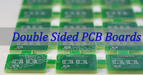
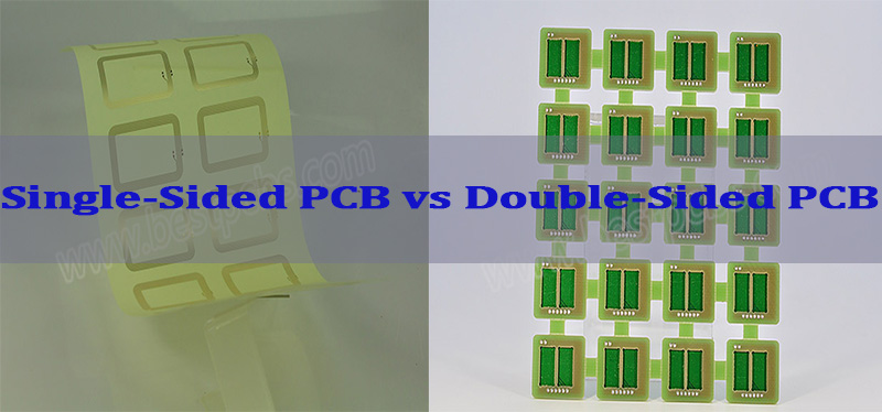
Double sided PCB boards are foundational components that enable complex and compact electronic circuits by providing conductive pathways on both sides of an insulating substrate. This article explores their structure, manufacturing, design, applications, and the critical role they play in building reliable modern electronics.
Balancing performance, reliability, and cost when sourcing double sided printed circuit boards remains a common challenge for engineers and procurement teams.
Inconsistent board quality paired with high cost or long lead times
Increased design complexity around vias and component placement
Risk of defects from poor plating or layer misalignment
Difficulty matching material performance to application needs
Slow or expensive prototyping cycles
These challenges underscore the importance of working with a manufacturer that addresses quality, design, and delivery together.
Strict process control ensures consistent quality from prototype to volume
Engineering support simplifies layout through DRC and DFM checks
Precision drilling and plating deliver reliable vias and alignment
Material options tailored to electrical and thermal requirements
Fast-turn prototyping enables quick and cost-effective validation
At EBest Circuit (Best Technology), we are a specialized double sided PCB board manufacturer in China committed to excellence. With over two decades of experience, we combine advanced manufacturing capabilities with rigorous quality control to produce reliable, high-performance PCBs. We understand that your electronics are only as good as their foundation, which is why we focus on delivering precision, consistency, and outstanding value for every order, big or small. Pls feel free to contact us at sales@bestpcbs.com to discuss your PCB or PCBA project needs. Our capabilities span FR4 PCB fabrication, flexible and rigid-flex circuitry, metal core and ceramic PCBs, supported by PCB layout and box-build integration.
What Are Double Sided PCB Boards?
A Double Sided PCB (Printed Circuit Board) is a circuit board that has conductive copper layers on both the top and bottom sides of an insulating substrate. The two layers are electrically connected using plated-through holes (PTHs), commonly known as vias. This simple yet powerful architecture allows circuits to cross over each other by moving from one side to the other, enabling more complex and dense circuitry than what is possible with a single sided PCB board.
Core Structure: An insulating core (like FR4) clad with copper foil on both sides.
Key Feature: Use of vias (holes plated with conductive material) to create electrical connections between the top and bottom layers.
Primary Benefit: Doubles the available area for routing traces compared to single-sided boards, allowing for more sophisticated circuits in a similar footprint.
In summary, double sided PCB boards serve as a critical stepping stone between simple single-layer boards and complex multi-layer boards, offering an optimal balance of functionality, cost, and manufacturing complexity for a vast array of electronic devices.
What Is the Difference Between Single and Double Sided PCB?
The fundamental difference between a single sided PCB and a double sided PCB lies in copper layer availability and routing flexibility. This distinction directly impacts circuit density, design freedom, manufacturing complexity, and overall cost, making it a key decision point during early PCB design.
Single vs Double Sided PCB Comparison
Feature
Single-Sided PCB
Double-Sided PCB
Copper Layers
1
2
Circuit Density
Low
Medium
Routing Capability
Limited
More flexible
Via Usage
Not required
Required
Design Complexity
Simple
Moderate
Cost Level
Low
Medium
Typical Applications
Basic circuits
Moderate-complex circuits
Manufacturing Steps
Basic etching
Drilling + through-hole plating
Practical Design Interpretation
A single sided PCB places all copper traces on one surface, which inherently limits routing options. Once traces begin to intersect or component density increases, designers quickly encounter layout constraints. This is why single sided designs are typically used in low-complexity products such as simple power supplies, LED boards, and basic consumer electronics.
In contrast, double sided PCB boards utilize copper on both the top and bottom layers. Electrical connections between the two sides are achieved through plated through-holes, allowing traces to cross layers without interference. This added routing freedom enables higher component density and more compact layouts without the cost escalation associated with multilayer PCBs.
From a cost–performance standpoint, double sided PCBs represent a balanced solution. They are more expensive than single sided boards due to additional drilling and plating steps, but they remain significantly more economical than multilayer constructions. As a result, they are widely adopted in consumer electronics, automotive control modules, industrial equipment, and communication devices.
In practice, when circuit requirements exceed the routing capacity of a single copper layer, double sided PCB boards become the logical next step. They provide improved electrical routing, better space utilization, and broader application flexibility while maintaining manageable manufacturing costs.
How Are Double Sided Copper Clad Board Structured?
A double sided copper clad board is the raw material from which finished PCBs are made. Its structure is the foundation of the board’s performance.
The basic structure consists of three key layers:
Top Copper Layer: A thin foil of conductive copper, typically 0.5 oz to 2 oz in weight, that will be etched to form the circuit pattern.
Dielectric Substrate Core: The insulating layer that provides mechanical support and electrical isolation. FR4 glass epoxy is the most common material.
Bottom Copper Layer: A second copper foil layer identical to the top, allowing for circuitry on both sides.
For the finished PCB, additional elements are added:
Solder Mask: A protective polymer layer (usually green) applied over the copper traces, leaving only the pads and vias exposed.
Silkscreen: The white lettering used for component labels, logos, and test points.
Surface Finish: A coating (like HASL, ENIG, or OSP) applied to exposed copper to prevent oxidation and enhance solderability.
Plated-Through Holes (PTHs): The metallized holes that connect the top and bottom copper layers, forming the essential 3D interconnect pathway.
This layered structure of a double-sided copper clad laminate PCB circuit board is precisely engineered to provide reliable electrical performance and mechanical stability.
How Is the Double-Sided PCB Manufacturing Process?
The double-sided PCB manufacturing process involves a series of precise steps to transform a raw double sided copper clad laminate into a functional circuit board.
Core Process Steps:
Drilling: Precise CNC machines drill holes for component leads and, critically, for vias that will connect both layers.
Through-Hole Plating: This is the defining step for double-sided boards. The drilled holes are chemically coated with a thin layer of copper, creating an electrical conduit between the top and bottom layers.
Imaging & Pattern Transfer: A photoresist is applied, and the circuit design is transferred using UV light through a photomask. The exposed (or unexposed, depending on the process) resist is then developed away.
Etching: The board is immersed in a chemical etchant (e.g., ferric chloride) which removes the unwanted copper, leaving only the desired circuit traces protected by the resist.
Stripping & Cleaning: The remaining photoresist is stripped off, revealing the copper circuitry.
Solder Mask Application: The solder mask ink is applied, exposed, and developed to open windows over pads and vias.
Surface Finishing: A final coating (e.g., ENIG, HASL) is applied to the exposed copper to ensure solderability and protect against corrosion.
Silkscreen & Electrical Test: Component labels are printed, and each board undergoes electrical testing to verify connectivity and the absence of short circuits.
In closing, this multi-stage process, especially the through-hole plating, is what enables the functionality of double sided PCB boards, ensuring reliable vertical interconnects that are crucial for their operation.
What Materials Are Commonly Used in Double Sided Printed Circuit Boards PCB?
The choice of material directly impacts the performance, reliability, and cost of the final board. The most common material is FR4, but alternatives exist for specific needs.
Standard Material:
FR4 (Flame Retardant 4): A composite of woven fiberglass cloth and an epoxy resin binder. It is the industry workhorse due to its excellent mechanical strength, good electrical insulation, moisture resistance, and relatively low double sided PCB board price.
Polyimide: Used for double sided flexible PCB board applications where the board must bend or flex.
Rogers or Taconic Laminates: High-frequency materials with stable dielectric constants for RF/microwave applications.
Metal-Clad (e.g., Aluminum): Used for boards requiring excellent thermal dissipation (LED lighting, power converters).
94V0 Rated FR4: A specific flammability rating (double-sided 94V0 PCB board) required for certain safety-critical applications.
To sum up, selecting the right base material—whether standard FR4 double-sided PCB board or a specialized alternative—is a critical first step in designing a reliable double sided copper PCB circuit board for any application.
What Design Rules Apply to Double Sided Printed Circuit Boards PCB Boards?
Effective double sided PCB design requires adhering to a set of rules to ensure manufacturability, reliability, and performance. These rules are often defined as Design for Manufacturability (DFM) guidelines.
Key Design Rules to Follow:
Trace Width/Spacing: Determine based on current carrying capacity and voltage. General rules (e.g., 6/6 mil for signal traces) must be confirmed with your manufacturer’s capabilities.
Via Specifications: Define hole size (drill diameter) and pad size (annular ring). Ensure the annular ring is sufficient to guarantee a reliable connection after drilling tolerances.
Component Placement: Place components logically, typically on the top side. Consider soldering process (wave soldering may require specific bottom-side component orientation).
Layer Coordination: Use one layer primarily for horizontal traces and the other for vertical traces to simplify routing. Assign one layer as a ground plane if possible for better noise immunity.
Thermal Management: Provide adequate thermal relief for pads connected to large copper pours (planes) to prevent solder issues during assembly.
Solder Mask & Silkscreen: Clearly define solder mask expansion and ensure silkscreen text does not cover pads.
To wrap up, by following these double sided PCB design rules and consulting your manufacturer’s DFM guidelines early, you can avoid costly delays and ensure your custom double sided PCB board is produced correctly the first time.
How Do Copper PCB Board Double Sided Perform Electrically and Thermally?
The performance of a double sided copper PCB board is intrinsically linked to its material properties and construction.
Electrical Performance:
Conductivity: The copper traces provide low-resistance pathways for electrical signals and power. Thicker copper (e.g., 2 oz) lowers resistance for high-current paths.
Signal Integrity: The proximity of traces on two layers can lead to crosstalk. Proper spacing, use of ground pours, and careful routing are essential. The dielectric constant (Dk) of the substrate material affects signal speed.
Impedance Control: For high-speed signals, the trace geometry (width, thickness) and distance to the reference plane (in more complex stack-ups) must be controlled to achieve a target impedance.
Thermal Performance:
Heat Dissipation: Copper is an excellent thermal conductor. Double sided copper PCB boards can dissipate heat more effectively than single-sided boards by using large copper areas (pours) on both layers.
Thermal Vias: Arrays of vias filled or plugged with thermal paste can be used to transfer heat from a component on the top layer to a large copper area on the bottom layer, significantly improving cooling.
Material CTE: The Coefficient of Thermal Expansion (CTE) of the substrate should be matched to components (like BGAs) to prevent solder joint stress during temperature cycling.
In brief, the structural advantages of a double sided copper clad PCB board—namely, the dual conductive layers and through-hole vias—provide designers with powerful tools to manage both electrical signal quality and thermal energy, which are crucial for reliable electronics.
What Are the Advantages of a Double Layer PCB?
Choosing a double sided PCB board over a single-sided one offers several compelling benefits that justify its slightly higher cost for many applications.
Core Advantages:
Increased Circuit Density: The primary advantage. Two layers allow traces to cross by switching sides via vias, accommodating more components and complex circuitry in a smaller area.
Enhanced Design Flexibility: Designers are not constrained by the routing limitations of a single layer, allowing for more optimized and efficient layouts.
Improved Signal and Power Integrity: The bottom layer can be used as a dedicated ground plane or power plane, reducing electromagnetic interference (EMI), crosstalk, and providing a stable reference for signals.
Better Thermal Management: The additional copper layer acts as a heat spreader. Thermal vias can be used to conduct heat away from hot components to the opposite side or to an external heatsink.
Reduced Overall Size and Weight: By enabling higher density, the physical footprint of the electronic assembly can often be reduced.
Cost-Effective Complexity: For circuits too complex for a single layer but not demanding enough for a multilayer PCB, double-sided boards offer the perfect balance of capability and double sided PCB boards cost.
In summary, these advantages make double sided printed circuit boards (PCB) the most popular and versatile board type, widely used across consumer, industrial, and automotive electronics.
How to Use Double Sided PCB Board
Using a finished double sided PCB board involves the standard electronics assembly process. Knowing how to use double sided PCB prototyping board is specifically crucial for developers.
For Finished/Production Boards:
Component Procurement: Gather all components (resistors, ICs, connectors) per the Bill of Materials (BOM).
Soldering: Apply solder paste to pads (for SMDs), place components, and use a reflow oven or hot plate. For through-hole components, insert leads and solder manually or via wave soldering.
Inspection & Testing: Visually inspect for solder bridges or tombstoning. Perform in-circuit testing (ICT) or functional testing.
How to Use Double Sided PCB Prototyping Board:
Prototyping boards, or perfboards, are pre-drilled boards with copper pads or strips. Here’s how to use them:
Planning: Map your circuit diagram onto the physical board. Use the top and bottom sides strategically for different parts of the circuit.
Component Placement: Insert component leads through the holes from the top side.
Interconnection: On the bottom side, use insulated wires or the existing copper patterns to make connections. The key step for double-sided boards is creating connections between the two sides.
Creating Vias: To connect a trace from the top to the bottom, use a small piece of solid wire (a “via wire”). Solder one end to the pad/trace on the top, pass the wire through a nearby hole, and solder it to the corresponding pad/trace on the bottom.
Testing: Continuously test sections of your circuit as you build to isolate faults.
To summarize, whether using a custom fabricated board or a universal double sided prototype PCB universal printed circuit board, the principle remains: leverage both sides for routing and use reliable methods (manufactured PTHs or manual via wires) to interconnect them.
Where Are Double Sided Copper Clad Laminate PCB Circuit Board Commonly Used?
The versatility of double sided copper clad laminate PCB circuit boards makes them ubiquitous in modern electronics. Their double-sided PCB applications span nearly every industry.
Common Application Areas:
Consumer Electronics: Power supplies, audio amplifiers, gaming peripherals, and smart home devices.
Automotive Electronics: Engine control units (ECUs), LED lighting modules, infotainment systems, and sensor interfaces.
Industrial Controls: PLCs, motor drives, power converters, and instrumentation panels.
Telecommunications: Routers, modems, network switches, and RF modules (often using specialized high-frequency laminates).
Medical Devices: Patient monitors, diagnostic equipment, and portable medical tools.
Prototyping & R&D: The double sided PCB prototyping board is a staple in engineering labs for developing and testing new circuit ideas.
To draw this to a close, from the cheap double sided PCB board in a toy to the robust board in an automotive module, double-sided technology is the backbone of a massive range of electronic products due to its optimal cost-to-performance ratio.
What Quality Factors Determine the Reliability of Double Sided Copper PCB Circuit Board?
The reliability of a double sided copper PCB circuit board is not accidental; it is engineered through strict control of several quality factors.
Critical Quality Factors:
Copper Plating Quality: The integrity of the plated-through holes (PTHs) is paramount. Voids, cracks, or insufficient plating thickness in the barrel of the hole can lead to intermittent or open connections.
Layer-to-Layer Registration: Precise alignment between the top and bottom layers and the drilled holes is essential. Misregistration can cause broken annular rings or shorts.
Material Integrity: The substrate must be free of voids/delamination and have the specified Tg, dielectric constant, and flame retardancy (e.g., 94V0).
Solder Mask Adhesion: The solder mask must properly adhere to the copper and substrate, with precise opening over pads. Poor adhesion can lead to mask peeling and solder bridging.
Surface Finish Durability: The finish (ENIG, HASL, etc.) must protect the copper from oxidation and provide a reliable, solderable surface throughout the product’s shelf life and assembly process.
Electrical Test Coverage: 100% electrical testing (flying probe or fixture-based) is crucial to verify continuity (no opens) and isolation (no shorts) across the entire board.
As a final remark, a reliable high-quality double sided PCB board is the result of meticulous attention to these factors throughout the double-sided PCB manufacturing process, ensuring the final product performs consistently in its end application.
To encapsulate the discussion, double sided PCB boards are the essential bridge between simple and highly complex circuits, providing the critical foundation for countless modern electronic devices. This article has explored their design, manufacturing, materials, and the key factors that define their quality and reliability.
For your next project that demands robust, compact, and cost-effective circuitry, a well-designed double sided printed circuit board (PCB) is likely the optimal solution. Partnering with an experienced manufacturer is key to unlocking this potential.
EBest Circuit (Best Technology) specializes in delivering high-quality, reliable double sided PCB boards. As a trusted China double sided PCB board manufacturer, we provide comprehensive support from double sided PCB board prototype to full-scale production, ensuring your electronics are built on a foundation of quality. Pls feel free to contact us anytime for a quote or technical consultation via sales@bestpcbs.com
FAQs
Q: What Is the Double Sided Copper Clad PCB Board?
A: It refers to the raw, un-etched base material—an insulating substrate (like FR4) with a layer of copper foil laminated to both of its sides. It is the starting point for manufacturing a finished double sided PCB board.
Q: What Are the Two Sides of a PCB Called?
A: They are conventionally called the Top Layer (or Component Side) and the Bottom Layer (or Solder Side). The Top Layer is usually where most components are placed.
Q: What Is a Single Sided PCB Used For?
A: A single sided PCB is used for very simple, low-cost electronic circuits where component count and routing are minimal, such as in basic power supplies, calculators, toys, and LED light boards.
Q: Are Motherboards Just PCBs?
A: Motherboards are a highly complex type of PCB. They are typically multilayer circuit boards (often 6-12 layers or more), integrating double sided PCB technology within a much denser stack-up to accommodate CPUs, RAM, and high-speed buses.
Q: What Is V in PCB Board?
A: “V” often refers to Voltage. In specific contexts like “94V0,” it is a flammability rating (UL94-V0) indicating the material’s ability to self-extinguish, a critical safety standard for PCBs.
Q: What Is a Trace on a PCB?
A: A trace is the conductive pathway, typically made of copper, etched onto the PCB substrate. It functions as the “wire” that carries electrical signals and power between components.
Q: How Do I Make a Double Sided PCB Board?
A: While hobbyists can make simple boards using toner transfer and chemical etching, producing reliable double sided PCB boards with plated-through holes requires professional equipment. The professional process involves: 1) Drilling holes, 2) Electroless copper deposition to make holes conductive, 3) Electroplating to build up copper, 4) Photoresist imaging, 5) Etching, and 6) Applying solder mask and finish. For reliable results, it is recommended to use a professional double sided PCB board factory in China like EBest Circuit.
Hungary has emerged as a key hub for electronics manufacturing in Eastern Europe, attracting numerous PCB Hungary manufacturer and global firms setting up local production bases. As a professional PCB Hungary manufacturer, EBest Circuit Co., Limited (Best Technology Circuit Co., Limited) leverages local industrial advantages and global supply chain resources to deliver high-quality PCB Hungary solutions. The region’s PCB manufacturing sector benefits from labor cost advantages and proximity to European markets, while facing challenges like process consistency and supply chain stability that demand reliable Hungary PCB manufacturer partners.
Are You Facing These Challenges?
Are your PCB designs frequently rejected due to manufacturability issues, leading to repeated revisions and project delays?
Are you unable to find a Hungarian PCB factory that can provide 24-hour expedited prototyping services for small-batch, time-sensitive orders?
Do you encounter board warping and deformation issues after lamination or reflow soldering, affecting assembly yield?
Do you frequently experience communication difficulties with local Hungarian PCB companies, resulting in mismatched production requirements?
Are high raw material costs and exchange rate fluctuations making it difficult to control your Hungarian PCB manufacturing costs?
Is the quality inspection of your mass-produced PCBs insufficient, leading to a risk of defects after delivery?
Are you unable to obtain timely technical support in Hungary for specialized processes such as HDI or thick copper PCB manufacturing?
End-to-End Guarantee from Requirement to Delivery
Pre-Production Consultation: Provide free DFM analysis to identify design flaws in advance, avoiding revision delays and reducing Hungary PCB manufacturing costs. Our professional team delivers analysis reports with clear optimization suggestions for seamless cooperation.
Urgent Prototyping Support: 24-hour rapid prototyping service for time-sensitive orders, ensuring your project progresses as scheduled without waiting for standard lead times. We leverage global production resources to fulfill urgent demands for PCB Hungary projects.
Process Optimization: Adopt symmetric lamination and precise temperature control to eliminate board warpage, improving assembly yield for PCB Hungary products. Strict process parameters are standardized to ensure consistent quality across batches.
Dedicated Account Management: Assign exclusive account managers to handle your orders, providing scheduled progress updates and prompt responses to inquiries via email and phone. We ensure production requirements are accurately implemented through our global production network for Hungary-bound orders.
Cost Control: Offer cost-sensitive solutions based on 19 years of experience, optimizing material selection and process flow to offset raw material and exchange rate impacts. Customized plans help reduce overall Hungary PCB manufacturing costs effectively.
Full Inspection for Mass Production: Implement 100% AOI and X-Ray inspection in our PCB manufacturing process for Hungary orders, eliminating defective products before delivery. Inspection reports are provided to confirm quality compliance.
Special Process Capability: Master HDI, thick copper, and rigid-flex PCB technologies, with a professional technical team to solve bottlenecks. We support complex process requirements for Hungary PCB manufacturing projects.
On-Time Delivery Commitment: Rely on mature global supply chain management and automated production lines to achieve a 99.2% on-time delivery rate. Cross-border logistics optimization ensures timely arrival of PCB Hungary orders.
Why Hungarian Clients Choose EBest (Best Technology) for PCB Manufacturer?
19 Years of Industry Experience: Rich expertise in solving complex manufacturing challenges, helping customers reduce trial-and-error costs and shorten time-to-market.
Free DFM Analysis: Professional design review before production, identifying potential issues to avoid rework and improve Hungary PCB manufacturing efficiency.
24-Hour Urgent Prototyping: Dedicated production lines for emergency orders, completing PCB Hungary prototyping within 24 hours to meet tight project schedules.
Authoritative Certifications: Hold ISO9001:2015, ISO13485:2016, IATF16949, REACH, and RoHS certifications, meeting requirements for medical, automotive, and industrial electronics.
Competitive Pricing & Cost-Saving Solutions: Customized cost-sensitive plans based on project requirements, reducing overall Hungary PCB manufacturing costs by 15%-20% through process optimization.
High On-Time Delivery Rate: 99.2% order punctuality supported by MES production management system, ensuring stable supply for your production line.
Strict Quality Control: 100% full inspection for mass production, adhering to strict quality control processes that exceed industry standards for PCB Hungary products.
Verify Certification Compliance: Confirm IATF16949 (automotive) and ISO13485 (medical) certifications. Ensure EU RoHS (lead ≤0.1%) and REACH compliance, aligning with your product category to avoid penalties from misaligned credentials (impacting 12% of local orders yearly).
Test Urgent Prototyping Capability: Validate 24-hour quick-turn services via small trials. Confirm dedicated lines, ≥99.2% urgent prototyping yield, and transparent costs with urgent fees at 15%-30% of standard pricing. Avoid hidden fees with detailed quotes covering all process costs.
Review Quality Control Details: Request AOI (≥99.8% surface defect coverage) and X-Ray (≥99.5% BGA joints accuracy) data. Target batch defect rate ≤0.05% (half the 0.1% industry average), and clarify 48-hour quality response and replacement for batches over 0.03% defects.
Confirm Process Suitability: Ask for verifiable Hungary project cases for HDI, thick copper or high-frequency PCBs. Ensure impedance tolerance ±5%, micro-drill tolerance ±0.01mm, layer alignment error ≤5μm, and dielectric constant 3.5-4.5 for high-frequency PCBs.
Assess Delivery Stability: Check 12-month on-time rate ≥98% (exceeding the 95% local average). Inquire about supply chain contingencies, including local core material stock (minimum 2 weeks) and logistics partners with ≥99% on-time rates, plus ≤2% annual disruption rate.
Prioritize Value-Added Services: Optimize for free 1-hour DFM analysis, which cuts rework rates from 8%-12% to ≤3%. Ensure ≥95% 24-hour resolution for complex processes; DFM analysis also shortens lead time by 3-5 days on average.
Analyze Total Cycle Costs: Beyond unit prices, account for rework (7% of order value), late fees (1%-2% daily), packaging (2%-5%), and EU customs duties (0%-6%). Prefer 3-6 month price locks to mitigate volatility, as copper prices fluctuate ±18% yearly.
Clarify Communication Norms: Set 24-hour email response timelines and 99.9% accurate notifications for key order nodes. Define 8-hour confirmation for order adjustments, reducing delays from miscommunication (affecting 6% of orders).
How to Evaluate Production Capacity of PCB Hungary Manufacturer?
Inspect Equipment Precision & Efficiency: Verify automated SMT lines with ≥60,000 components/hour placement speed and ±0.03mm precision, AOI machines with ≥99.8% surface defect coverage, and micro-drilling equipment supporting minimum 0.1mm diameter with ±0.01mm tolerance.
Review Process Parameter Limits: Confirm maximum production layers (1-20 layers for high-capacity Hungary PCB factory), minimum line width 0.075mm, and minimum hole diameter 0.1mm, with impedance tolerance controlled within ±5% for high-frequency products.
Evaluate Daily Capacity & Batch Adaptability: Assess daily output (5,000-50,000 pieces for mass production, 100-500 pieces for small-batch) and order handling capability, ensuring ≤24-hour response for batches ≤500 pieces and stable yield ≥99.2% across batch sizes.
Check Supply Chain Stability: Confirm cooperation with top-tier material suppliers (e.g., Isola, Rogers for substrates; JX Nippon for copper foil), core material inventory ≥14 days, and supplier on-time delivery rate ≥99% to avoid production interruptions.
Assess Process Optimization Efficiency: Evaluate multi-variety order changeover time (≤2 hours for different PCB types) and process optimization effects, such as yield improvement ≥3% and production cycle reduction ≥15% via smart process adjustment.
Verify Quality Management Effectiveness: Check batch defective rate ≤0.05% (industry average 0.1%), customer complaint rate ≤0.3%, and ISO9001:2015-certified QMS with monthly quality review mechanisms.
Quantify Technical Problem-Solving Capacity: Confirm technical team size (≥15 professionals for mid-sized Hungary PCB manufacturer), complex process problem-solving rate ≥95%, and resolution time ≤24 hours for HDI/thick copper PCB issues.
Evaluate Scheduling & Urgent Order Flexibility: Ensure MES-based production scheduling system with real-time tracking, ≤2-hour response to urgent orders, and ability to handle ≤30% urgent orders without affecting standard order on-time rate (≥98%).
How to Evaluate Delivery Time of Hungary PCB Manufacturer?
Confirm standard delivery times: Clearly define delivery times for different order types and layer counts – prototyping (1-8 layers: 2-5 days; 10+ layers: 7-10 days) and mass production (1-8 layers: 3-8 days; 10+ layers: 10-15 days), consistent with the average standards of the Hungarian PCB manufacturing industry.
Assess urgent order handling capabilities: Verify 24/48-hour delivery capabilities, with urgent order fees at 15%-30% of the standard price. Ensure on-time delivery rate for urgent orders is ≥99%, and that a dedicated production line is available to support up to 30% of daily capacity.
Check on-time delivery rate: Require an on-time delivery rate of ≥98% over 12 months, higher than the local industry average of 95%. Require detailed data, with delays due to logistics reasons accounting for ≤60% and delays due to production reasons accounting for ≤40%.
Assess supply chain resilience: Confirm safety stock of core materials (copper foil, substrates) is ≥14 days. Ensure annual logistics disruption rate is ≤2%, and that an emergency plan for raw material shortages is in place with a 48-hour recovery capability.
Review scheduling transparency: Ensure real-time tracking based on the MES system, with order status updated every 4 hours. Require order visualization coverage of ≥99%, and respond to scheduling adjustment requests within 8 hours.
Inquire about delay contingency plans: Inquire about the capacity of backup production lines (which can be activated within 2 hours), representing 20% of total capacity. Clearly define delay compensation terms, typically 1%-2% of the order value per day.
Evaluate logistics partners: Verify that logistics partners have an on-time delivery rate of ≥99%. Confirm domestic delivery time in Hungary is within 24 hours, and cross-border delivery time in Europe is within 48-72 hours, with logistics costs ≤5% of the order value.
Check communication efficiency: Ensure delay notifications are sent within 2 hours of discovering a delay. Require delivery milestone reminder coverage of ≥99.5%, and respond to status inquiry emails within 24 hours.
FAQs of Hungary PCB Manufacturing
Q1: How to solve board warpage problems during Hungary PCB manufacturing? A1: We adopt symmetric lamination design and precise temperature control during reflow soldering (heating rate ≤2℃/sec, cooling rate ≤1℃/sec) to eliminate internal stress. Our pre-production DFM analysis also optimizes copper distribution to prevent warpage. Contact us for customized process solutions for your PCB Hungary project.
Q2: Why do design files often cause production delays, and how to avoid it? A2: Common issues include unclear layer definitions and insufficient pad spacing. We provide free DFM analysis to check design files within 1 hour, identifying and correcting flaws in advance. Our team will also offer optimization suggestions to ensure smooth Hungary PCB manufacturing. Inquiry now for free file review.
Q3: How to control costs when raw material prices and exchange rates fluctuate? A3: With 19 years of experience, we offer cost-sensitive solutions by optimizing material selection and process flow. We also lock in material prices for long-term cooperation and share cost-saving tips. Choose our PCB manufacturing service Hungary to stabilize your budget. Contact us for a quotation.
Q4: What to do if urgent prototyping is needed within 24 hours for a small-batch order? A4: Our Hungary PCB plant has dedicated urgent production lines, completing 24-hour prototyping for 1-20 layers of PCB. We also provide door-to-door delivery in Hungary to save time. Reach out now to start your urgent PCB Hungary order.
Q5: How to ensure quality consistency for mass-produced PCBs? A5: We implement 100% AOI optical inspection and X-Ray detection for BGA solder joints, with a strict three-stage quality control process. Our batch defective rate is controlled below 0.03%, meeting high industry standards. Trust our PCB Hungary manufacturer for stable quality—send your inquiry today.
FFC vs FPC connector is a critical component in modern electronics, enabling reliable connections for flexible circuits. This article will compare their differences, address common application challenges, and guide you in selecting the right solution for your flexible flat cable needs.
Are you struggling with signal integrity, mechanical failures, or assembly headaches in your flexible circuit designs? Many engineers face significant hurdles when integrating FFC and FPC connectors into their products.
Intermittent connections or signal loss due to poorly mating connectors and cables.
Difficulty in manual assembly, leading to damaged cable ends or connector latches.
Confusion between FFC vs FPC cable specifications, resulting in mismatched components.
Signal interference in high-speed applications using standard FFC ribbon cables.
Mechanical stress causing failure at the connector junction in dynamic flexing applications.
The solution lies in a clear understanding of the FFC FPC difference and partnering with a manufacturer that masters their application. As an experienced FPC and PCBA manufacturer, EBest Circuit (Best Technology) provides not just components but complete integration support.
Supplying precision-engineered FFC/FPC connectors and cables with guaranteed mating specifications.
Offering connectors with Zero Insertion Force (ZIF) or Low Insertion Force (LIF) mechanisms for error-proof assembly.
Providing expert guidance to clarify FFC vs FPC connector selection based on your specific current rating, spacing, and flexibility needs.
Recommending and sourcing shielded FPC ribbon cables or specific FPC connector types for EMI-sensitive designs.
Implementing robust strain relief and optimal board layout in our PCBA manufacturing to enhance flex endurance.
At EBest Circuit (Best Technology), we specialize in the manufacturing and assembly of high-quality Flexible Printed Circuits (FPC) and PCBAs. Our deep expertise in FFC/FPC connectors application ensures that your flexible interconnects are reliable, durable, and perfectly suited to your design’s mechanical and electrical demands. For your next project, pls feel free to contact our team at sales@bestpcbs.com.
What Is the Difference Between FFC vs FPC Connector?
The core difference lies in what they connect. An FPC connector is the receptacle soldered onto a PCB, designed to accept a flexible conductor. FFC, meaning Flexible Flat Cable, is the removable cable that plugs into that connector. Think of FPC vs FFC connector as a socket versus a plug. The connector’s design must match the cable’s specifications.
FPC Connector Types: These are defined by their actuation method (ZIF, LIF, Non-ZIF) and contact orientation (top, bottom, double-sided).
FFC Cable Specs: Defined by pitch (e.g., 0.5mm, 1.0mm), pin count (FFC cable 6 pin, 8 pin, 30 pin, etc.), length, and thickness.
In summary, the FFC vs FPC comparison is symbiotic: the connector is the interface, and the cable is the conductor. Selecting the correct pair is foundational to system reliability.
What Is the Relationship Between FFC and FPC Connectors?
Their relationship is defined by mechanical and electrical compatibility. They form a complete interconnect system. The FPC connector is engineered to precisely match the physical dimensions and electrical parameters of the FFC cable.
Pitch Compatibility: The connector’s contact spacing must exactly match the cable’s conductor pitch (e.g., a 1.0mm pitch connector for a 1.0mm pitch FFC cable 4 pin).
Thickness Compatibility: The connector’s clamp must accommodate the total thickness of the flexible flat cable FFC.
Circuit Alignment: The connector’s contacts must align with the cable’s conductors. Some connectors are for “straight” access, others for “right-angle” mating.
Actuation Mechanism: The cable is inserted and locked using the connector’s latch (ZIF) or a simple friction fit.
The key takeaway is that they are not interchangeable without verifying specs. A mismatch, even by a few microns, can cause poor contact or mechanical failure.
What Is the Purpose of FFC Cable in Flexible Flat Cable Connector Design?
The purpose of the FFC cable is to provide a reliable, flexible, and cost-effective conductive link between two PCBs or components within an assembly. Its design directly influences the flexible flat cable connector choice.
Space Savings: Enables dense, three-dimensional packaging impossible with round wires.
Reliability: Eliminates the risk of individual wire misplacement during assembly vs discrete wiring.
Mass Termination: All conductors are connected simultaneously upon insertion, drastically reducing assembly time and cost.
Controlled Impedance: In high-speed designs, FPC ribbon cables can be engineered for specific impedance.
Repeatable Flexing: Designed to withstand repeated bending in applications like hinge connections.
Therefore, the FFC cable is the enabling element for modular design and servicing, while the connector ensures its secure and stable interface.
What Are the Common FPC Connector Problems?
Several issues can plague FPC connector applications, often stemming from selection, handling, or manufacturing flaws.
Poor Contact/Intermittency: Caused by contaminated contacts, mismatched cable thickness, or a worn/loose locking mechanism.
Cable Misalignment: The FFC cable is not fully inserted or is offset, leading to shorted or open circuits.
Damaged Latches: The ZIF/LIF latch is brittle and can break during assembly or disconnection if not handled properly.
Mechanical Stress: Bending or pulling stress concentrated at the connector-cable junction can tear the cable or break solder joints.
Soldering Issues: Poor solder joints on the connector’s PCB footprint (e.g., tombstoning, insufficient solder) can cause open circuits.
Understanding these failure modes is the first step in prevention through robust design and assembly practices.
How to Select the Right FFC/FPC Connectors for Your Application?
Selecting the right pair requires a systematic approach based on your design’s electrical, mechanical, and environmental needs.
Pin Count & Pitch: Determine the number of signals (FFC cable 30 pin) and the available space (pitch: 0.3mm, 0.5mm, 1.0mm).
Current Rating: Check the current per circuit. Standard FFC cables have lower current capacity than thicker custom FPC cables.
Stack Height: Measure the required space between boards to choose a connector with the correct mating height.
Flex Life & Direction: Define how often and in what direction the cable will bend. This affects cable construction.
Actuation Type: ZIF for frequent service, LIF/Non-ZIF for cost-sensitive, permanent applications.
Shielding Needs: For noisy environments, specify cables with shielding layers and corresponding shielded FPC connector types.
A careful evaluation against this checklist ensures a reliable FFC vs FPC cable interconnect system.
How Does the Choice Between FFC vs FPC Connector Impact FPC and PCBA Manufacturing?
The choice directly impacts DFM (Design for Manufacturability), assembly yield, and long-term reliability.
Soldering Profile: The connector’s plastic housing may have a lower maximum temperature than the PCB, requiring a controlled reflow profile.
Strain Relief Features: The design must include features like adhesive stickers, stiffeners, or board keep-outs to protect the connection point.
Test Accessibility: The connector’s location must allow for test probe access if needed.
Rework Difficulty: ZIF connectors are easier to rework than soldered cable ends, affecting serviceability and repair costs.
Integrating connector selection early in the design phase is crucial for manufacturability.
Why an Experienced FPC and PCBA Manufacturer Matters for FFC/FPC Connector Projects?
An experienced partner like EBest Circuit (Best Technology) bridges the gap between component selection and a flawless final product. We understand that FFC vs FPC connector success is about the entire ecosystem.
Holistic Design Review: We assess your schematic and layout for connector placement, strain relief, and potential signal integrity issues.
Component Sourcing & Verification: We procure genuine, compatible connectors and cables, verifying specs like pitch and thickness before assembly.
Process Optimization: Our assembly lines are calibrated for sensitive FPC connector placement and soldering.
Testing & Validation: We perform continuity, hipot, and functional tests to ensure every flexible flat cable connector interface is flawless.
Failure Analysis & Support: If issues arise, our expertise allows us to quickly diagnose whether it’s a connector, cable, or assembly problem.
This end-to-end control minimizes risk and ensures your product’s reliability from the first prototype to mass production.
All in all, FFC vs FPC connectors form the essential link between portability and functionality in modern electronics. This comparison has highlighted their distinct roles, common pitfalls, and selection criteria to ensure robust flexible applications.
Partnering with a manufacturer that possesses deep expertise in both FPC and PCBA manufacturing is crucial. EBest Circuit (Best Technology) provides the integrated design support, precision manufacturing, and quality assurance needed to navigate the complexities of FFC/FPC connectors successfully. Let us help you perfect your flexible interconnect design. Pls feel free to contact us anytime at sales@bestpcbs.com for a consultation on your next flexible PCB or SMT assembly project.
FAQs
Are FPC Connectors Waterproof?
Standard FPC connectors are not waterproof. They are designed for indoor, controlled environments. For moisture or dust exposure, you need specifically rated IP connectors or must use conformal coating and gasketing as a secondary sealing method.
Can FFC Cables Be Soldered?
Directly soldering an FFC cable is generally not recommended and defeats its purpose as a removable interconnect. The laminate insulation can melt, and the fine conductors are easily damaged. Always use a compatible FPC connector for a reliable, solderless connection.
What Are FPC Connectors Used For?
FPC connectors are used anywhere a compact, reliable, and flexible electrical connection is needed. Common applications include laptop displays (FFC cable 40 pin for LCDs), printers, scanners, cameras, medical devices, consumer electronics, and automotive dashboards where connecting PCBs across hinges or moving parts is required.
Custom PCB prototyping is the process of creating tailored printed circuit board prototypes designed to meet the unique needs of specific projects—whether for consumer electronics, industrial equipment, medical devices, or aerospace applications. In Toronto’s dynamic tech ecosystem, this service isn’t just about producing a basic board; it’s about translating complex design concepts into functional, testable prototypes that align with local industry standards and project timelines. Unlike off-the-shelf PCBs, custom PCB prototyping prioritizes flexibility: from choosing materials (FR4, metal-based PCBs, ceramic PCBs, or flexible PCBs) to optimizing layer counts, trace widths, and component placements. For Toronto-based engineers and startups, this means getting a prototype that fits their exact use case—whether it’s a compact board for a wearable device or a high-frequency PCB for communication equipment.
Custom PCB Prototyping vs. Standard PCB Manufacturing: Key Differences
When deciding between custom PCB prototyping and standard PCB manufacturing, understanding the core differences is critical for Toronto tech teams. Standard manufacturing focuses on mass-produced, generic boards with fixed specifications, ideal for high-volume production where consistency and cost-efficiency are top priorities. Custom PCB prototyping, by contrast, is built for low-volume, project-specific needs—prioritizing design flexibility, rapid iteration, and precision over scale.
In Toronto’s fast-paced innovation scene, this distinction matters: startups testing a new product concept need a prototype that can be modified quickly if adjustments are needed, while established firms might use custom prototyping to validate a complex design before full-scale production. Custom prototyping also offers tighter quality control for specialized applications (e.g., medical devices requiring ISO 13485:2016 compliance or aerospace components needing AS9100D certification)—a must for Toronto industries operating in regulated sectors.
Top Applications of Custom PCB Prototyping in Toronto’s Tech Industry
Toronto’s diverse tech landscape relies on custom PCB prototyping to drive innovation across key sectors. Here are the most common use cases:
Medical Devices: Prototypes for diagnostic tools, wearable health monitors, and implantable devices—requiring biocompatible materials and adherence to ISO 13485:2016 standards.
Aerospace & Defense: High-reliability PCBs for avionics systems, where resistance to extreme temperatures and vibration is non-negotiable (aligned with AS9100D requirements).
Consumer Electronics: Compact, high-performance prototypes for smartphones, IoT devices, and home automation products—prioritizing miniaturization and energy efficiency.
Industrial Automation: Robust PCBs for control systems, sensors, and manufacturing equipment, designed to withstand harsh factory environments.
Renewable Energy: Prototypes for solar inverters, battery management systems, and wind turbine controls—focused on durability and high-power handling.
For Toronto engineers, these applications demand prototypes that don’t just work—they work within the city’s regulatory frameworks and industry-specific needs.
How to Choose the Right Custom PCB Prototyping Partner in Toronto
Selecting a reliable custom PCB prototyping partner in Toronto can make or break your project. Here’s what to prioritize:
Industry Certifications
Look for partners with globally recognized certifications like IATF 16949, ISO 9001:2015, ISO 13485:2016, and AS9100D. These certifications prove adherence to strict quality and safety standards—critical for Toronto’s regulated industries. Additional compliance with REACH, RoHS, and UL standards ensures environmental and safety compliance.
Material & Technology Capabilities
Ensure the partner offers a range of substrates (FR4, metal-based PCBs (MCPCBs), ceramic PCBs, flexible and rigid-flexible PCBs) and can handle complex designs (multi-layer PCBs, high-frequency PCBs). Toronto projects often require specialized materials, so versatility is key.
Turnaround Time
Urgent projects need expedited service—look for partners that offer 24-hour shipping for critical prototypes. In Toronto’s competitive tech scene, fast iteration can mean the difference between leading the market and falling behind.
End-to-End Services
A full-service partner (offering PCB Design, PCB Prototype, Component Sourcing, PCB Assembly, and Box-Build-Assembly) streamlines the process, reducing communication gaps and ensuring consistency from concept to prototype.
Common Terms in Custom PCB Prototyping You Need to Know
Navigating custom PCB prototyping requires familiarity with key industry terms—essential for clear communication with your Toronto-based manufacturer:
FR4: The most common PCB substrate (glass-reinforced epoxy resin), ideal for general-purpose applications.
MCPCB (Metal-Core PCB): A substrate with a metal core (typically aluminum) for enhanced heat dissipation—used in LED lighting and power electronics.
Rigid-Flex PCB: A hybrid board combining rigid and flexible sections, perfect for compact or foldable devices.
Trace Width: The width of the conductive pathways on the PCB, critical for carrying electrical current without overheating.
SMT (Surface Mount Technology): A method of mounting components directly onto the PCB surface, enabling miniaturization.
Through-Hole Technology: Components with leads inserted through holes in the PCB—used for high-reliability applications.
DFM (Design for Manufacturability): The process of optimizing PCB designs to ensure efficient, cost-effective production.
Understanding these terms ensures you can articulate your project needs and evaluate prototype quality effectively.
FAQ: Common Custom PCB Prototyping Questions for Toronto Engineers
How long does custom PCB prototyping take in Toronto?
Typical turnaround time is 3–7 business days for standard prototypes, but expedited service (24–48 hours) is available for urgent projects. Factors like design complexity, layer count, and material availability can affect lead time.
What materials are best for custom PCB prototypes in Toronto?
FR4 is ideal for general-purpose projects, while MCPCBs are best for heat-sensitive applications (e.g., LEDs). Ceramic PCBs offer high-temperature resistance (for aerospace/medical use), and flexible/rigid-flexible PCBs work for compact or wearable devices.
Do I need to provide a complete design file for prototyping?
Yes—most manufacturers require Gerber files (the standard PCB design format) or CAD files. Reputable partners may offer PCB Design support if you need help refining your design.
Can custom prototypes be scaled to mass production?
Absolutely. A quality custom PCB prototyping partner will ensure your prototype is designed for manufacturability (DFM), making the transition to Mass Production seamless—critical for Toronto startups looking to scale quickly.
Are custom PCB prototypes compliant with Toronto/Canadian regulations?
Yes—if you choose a certified partner. Look for compliance with RoHS (Restriction of Hazardous Substances), REACH (Registration, Evaluation, Authorization and Restriction of Chemicals), and industry-specific standards (ISO 13485:2016 for medical, AS9100D for aerospace).
How much does custom PCB prototyping cost in Toronto?
Cost varies based on layer count, material, size, and quantity. Prototypes typically range from $50–$500 for low-volume orders. Discussing your project details with a partner will get you a precise quote.
What if my prototype fails testing?
A reliable partner will offer design reviews and DFM checks upfront to minimize failures. If issues arise, they should work with you to iterate on the design and produce a revised prototype quickly.
Key Challenges in Custom PCB Prototyping (and How to Overcome Them)
Even with a great design, custom PCB prototyping can present challenges—here’s how to address them for Toronto projects:
Design Complexity
Complex layouts (e.g., multi-layer PCBs, high-frequency traces) can lead to signal interference or manufacturing errors. Solution: Work with a partner that offers DFM reviews to identify issues early and optimize your design for production.
Material Shortages
Global supply chain issues can delay prototype production. Solution: Choose a partner with established Component Sourcing networks—they can secure rare materials or suggest suitable alternatives without compromising quality.
Tight Timelines
Urgent projects (e.g., product launches, client demos) require fast turnaround. Solution: Prioritize partners with expedited services and efficient production capabilities—avoiding long shipping times from international manufacturers.
Regulatory Compliance
Meeting industry standards (e.g., ISO 13485:2016, AS9100D) can be daunting. Solution: Select a certified partner that understands Toronto’s regulatory landscape—they’ll ensure your prototype meets all necessary compliance requirements (including REACH, RoHS, and UL).
The Importance of DFM (Design for Manufacturability) in Custom PCB Prototyping
Design for Manufacturability (DFM) is a critical step in custom PCB prototyping—yet it’s often overlooked. DFM involves optimizing your design to ensure it can be manufactured efficiently, reliably, and cost-effectively. For Toronto engineers, this means reducing the risk of production delays, costly reworks, and prototype failures.
A strong DFM process includes checking for trace width consistency, component placement (to avoid soldering issues), and material compatibility. Reputable prototyping partners will conduct DFM reviews as part of their service, flagging potential issues (e.g., overly narrow traces, incompatible components) and suggesting adjustments. This proactive approach saves time and money—especially for Toronto startups and small teams with limited resources.
Custom PCB Prototyping for High-Frequency Applications in Toronto
High-frequency PCBs (used in communication systems, radar, and IoT devices) require specialized custom PCB prototyping—and Toronto’s tech industry is increasingly demanding this expertise. High-frequency prototypes need substrates with low dielectric loss (e.g., PTFE) to minimize signal degradation, as well as precise trace spacing to avoid interference.
Manufacturers with experience in high-frequency prototyping understand the unique challenges: maintaining signal integrity, controlling impedance, and ensuring thermal management. Whether you’re developing a 5G device or a satellite communication system, a specialized partner will tailor the prototype to your frequency requirements (typically 1 GHz and above) and validate performance through testing.
How Custom PCB Prototyping Supports Toronto’s Startup Ecosystem
Toronto’s startup scene thrives on innovation—and custom PCB prototyping is a cornerstone of that success. Startups often have limited budgets and tight timelines, making prototyping a make-or-break step. Custom prototyping allows them to test ideas quickly, iterate on designs without committing to Mass Production, and validate product-market fit before scaling.
For example, a wearable tech startup can use a custom prototype to test a new sensor integration, while a cleantech startup can validate a battery management system design. Local prototyping partners offer the agility startups need: fast turnaround, flexible order quantities (even 1–10 boards), and personalized support. This accessibility levels the playing field, allowing Toronto startups to compete with larger firms and bring innovative products to market faster.
Quality Control in Custom PCB Prototyping: What Toronto Engineers Should Expect
Quality is non-negotiable in custom PCB prototyping—and Toronto engineers should demand rigorous quality control (QC) from their partner. A robust QC process includes:
Visual inspections to check for soldering defects, trace damage, or component misalignment.
Electrical testing (e.g., continuity testing, impedance testing) to ensure the prototype functions as intended.
Material verification to confirm substrates and components meet specified standards (e.g., RoHS compliance).
Environmental testing (for specialized applications) to validate performance in extreme temperatures, humidity, or vibration.
Certified partners (ISO 9001:2015, IATF 16949) follow standardized QC protocols, providing documentation to prove compliance. This transparency is critical for Toronto projects in regulated industries—ensuring your prototype is reliable, safe, and ready for testing.
Why Choose EBest Technology for Custom PCB Prototyping in Toronto
When it comes to custom PCB prototyping in Toronto, EBest Technology brings over 20 years of expertise, industry-leading certifications, and a customer-centric approach that sets us apart. Founded in 2006, we specialize in tailored solutions—from standard FR4 prototypes to complex multi-layer PCBs, high-frequency PCBs, metal-based PCBs (MCPCBs), ceramic PCBs, and flexible/rigid-flexible PCBs—all manufactured to meet IATF 16949, ISO 9001:2015, ISO 13485:2016, and AS9100D standards, with full compliance to REACH, RoHS, and UL. Our monthly production capacity of 260,000 square feet (28,900 square meters) means we can handle both small-batch prototypes and scale-up orders, while our 24-hour expedited service ensures your urgent projects stay on track.
We don’t just produce prototypes—we offer one-stop PCB solutions, partnering with you every step of the way: from PCB Design support and DFM reviews to Component Sourcing, PCB Assembly, and Box-Build-Assembly. Our team of engineers invests heavily in research and development to stay ahead of industry trends, focusing on product quality and customer satisfaction. We understand Toronto’s tech ecosystem and regulatory requirements, ensuring your prototype is not just functional, but optimized for your specific application. Whether you’re a startup testing a new concept or an established firm validating a complex design, we deliver reliable, high-quality prototypes that drive your project forward.
Don’t let prototyping delays or subpar quality hold you back. Contact EBest Technology today to discuss your custom PCB prototyping needs—we’ll provide a tailored quote, fast turnaround, and the expertise you need to turn your design into a successful product. With our personalized support and proven track record as a trusted global partner, we’re here to help you innovate with confidence. Let’s build something great together.