

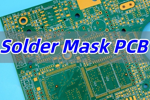
Solder mask PCB is a critical protective layer that safeguards your circuit boards. This guide explores how proper solder mask application prevents shorts, enhances durability, and ensures your PCB performs as intended, covering materials, process, thickness, and color selection.
So, where exactly do things go wrong for customers? Most solder mask issues are found late—often during assembly or testing.
- Peeling or bubbling raises rework rates. Heat during reflow or wave soldering can cause the mask to separate, leading to shorts or pad lift.
- Misaligned openings affect solder accuracy. Any shift between design and production can cause poor copper exposure or tiny solder bridges.
- Uneven thickness impacts fine-pitch parts. BGA or 01005 parts need stable mask thickness for proper solder wetting and balance.
- Unstable color hurts inspection. White or black solder masks may show shade or reflection differences, affecting AOI results.
- Poor material lowers long-term reliability. Low-grade epoxy can age and crack in harsh environments, reducing insulation performance.
EBest Circuit (Best Technology) provides full-process solutions to avoid these issues from the start.
- Strong adhesion: Plasma cleaning and auto coating keep the surface clean and the mask firmly attached.
- Accurate LDI exposure: Digital imaging keeps window tolerance within ±15 μm.
- Controlled thickness: Online monitoring avoids uneven coating.
- Stable ink quality: All inks come from trusted brands like Taiyo and Peters for consistent appearance.
- Reliable materials: Epoxy, PI, and UV-curing inks are tested for heat, moisture, and insulation to support automotive, medical, and LED use.
As a professional PCB manufacturer with over 19 years of experience, EBest Circuit (Best Technology) specializes in delivering high-quality boards that stand up to demanding applications. Our capabilities extend across advanced PCB types, including HDI, heavy copper, and high-frequency boards. We maintain certifications like ISO 9001, IATF 16949, ISO 13485, and AS9100D, ensuring every step of our process—from solder mask application to final electrical testing—meets the highest standards. Our engineering team provides dedicated support to optimize your design for manufacturability. For a seamless experience and boards you can trust, contact us at sales@bestpcbs.com.
Solder Mask PCB Meaning
At its core, the solder mask on a PCB is a thin, protective lacquer-like layer of polymer applied to the copper traces of a circuit board. Its primary function is to prevent solder from bridging between conductors during the component assembly process, thereby avoiding short circuits. However, its role extends far beyond just assembly aid.
- Electrical Insulation: The solder mask acts as a permanent insulator between adjacent copper traces. This is crucial for high-density designs where trace spacing is minimal, preventing current leakage and cross-talk at high frequencies.
- Environmental Protection: It shields the relatively delicate copper circuitry from oxidation, moisture, dust, and chemical contaminants. This protection is vital for the long-term reliability and longevity of the PCB, especially in harsh environments.
- Mechanical Support: The mask provides a degree of mechanical protection against minor scratches and abrasion during handling and assembly.
- Improved Solderability: By defining precise areas for soldering (the “solder mask openings” or “solder mask dams”), it helps control solder flow, leading to higher quality solder joints and facilitating automated assembly.
In essence, think of the solder mask as the PCB’s immune system. A robust, well-applied mask defends the board against a host of potential failures. A compromised one leaves the entire system vulnerable.
What is Solder Mask Opening?
A solder mask opening is a strategically placed window in the solder mask layer that exposes the underlying copper feature intended for soldering. These openings are fundamental to the PCB’s function and assembly.
- Purpose and Types:
- Component Pads: The most common type, these openings expose the copper pads where surface-mount (SMD) or through-hole components will be soldered.
- Test Points: Specific openings allow test probes to make electrical contact with the circuit for debugging and validation.
- Gold Fingers: The connecting edge of a board often has large openings plated with gold for reliable, wear-resistant contact.
- Heavy-Copper Areas: For boards carrying high current, larger openings may be used to allow for extra solder deposition, enhancing current-carrying capacity and heat dissipation.
- Design Considerations: The design of the opening is critical. An opening that is too small can lead to poor solder joint formation or tombstoning of components. A general rule of thumb is that the solder mask opening should be larger than the copper pad by a specific margin. For instance, a common specification is an expansion of 2 to 4 mils (0.05mm to 0.10mm) per side beyond the copper pad. This ensures adequate space for solder fillet formation without encroaching on the pad.
In summary, solder mask openings are the carefully planned gaps in the PCB’s protective armor, allowing for electrical connection and assembly while the rest of the board remains shielded.
What is PCB Solder Mask Material?
The choice of solder mask material directly impacts the board’s performance, durability, and manufacturability. The most prevalent type used today is Liquid Photoimageable Solder Mask (LPSM).
- Liquid Photoimageable Solder Mask (LPSM): This material is applied as a liquid and then hardened by exposure to UV light through a phototool. The unexposed areas are then developed away, creating the openings. LPSM offers high resolution, excellent adhesion, and good flexibility.
- Epoxy-Based: The most common formulation, known for its excellent chemical resistance, hardness, and adhesion. It is suitable for the vast majority of applications.
- Acrylic-Based: Offers easier reworkability but generally has lower chemical and thermal resistance compared to epoxy.
- Polyimide-Based: Used for flexible PCBs (flex and rigid-flex) due to its inherent flexibility and high-temperature endurance.
- Key Material Properties:
- Dielectric Strength: Typically >1000 V/mil, ensuring good electrical insulation.
- Thermal Resistance: Must withstand multiple soldering cycles (e.g., lead-free soldering at 260°C for 30-60 seconds) without degradation.
- Adhesion Strength: Measured via cross-hatch test, it should not peel from the substrate. High adhesion prevents delamination under thermal stress.
Selecting the right material is a balance between these properties and the specific requirements of the end application, such as the need for flexibility, extreme temperature cycling, or exposure to harsh chemicals.
Solder Mask PCB Machine
Modern solder mask application relies on sophisticated machinery to ensure consistency and quality. Two primary methods are dominant:
- Curtain Coating: Ideal for high-volume production of flat boards. The PCB is conveyed through a continuous curtain of liquid solder mask, resulting in a very uniform thickness. However, it is less effective for boards with significant topography or components already in place.
- Screen Printing: A versatile method where solder mask is forced through a fine mesh screen onto the PCB. It is well-suited for prototyping and medium-volume runs. While it can handle some uneven surfaces, achieving highly uniform thickness can be more challenging than with curtain coating.
The critical technological advancement in defining the mask pattern is Laser Direct Imaging (LDI). Instead of using a physical phototool, LDI uses a laser to directly expose the solder mask according to the digital design data. This eliminates alignment errors associated with phototools and allows for incredibly fine features, with resolutions capable of producing solder mask dams (the strip of mask between two adjacent pads) as narrow as 2 mils (0.05mm). This precision is essential for today’s high-density interconnect (HDI) designs.
What is PCB Solder Mask Process?
The application of solder mask is a multi-step, tightly controlled process. Here is a typical workflow:
- Pre-Cleaning: The bare copper board is thoroughly cleaned to remove oxides and contaminants, ensuring optimal adhesion of the solder mask.
- Application: The liquid solder mask is applied via screen printing or curtain coating.
- Pre-Baking (Tack Drying): The board is passed through a low-temperature oven to evaporate solvents, leaving a “tack-dry” surface that is no longer liquid but not fully cured.
- Exposure: The board is exposed to UV light. For traditional methods, a phototool (film) is used. For higher precision, LDI is employed. The UV light cross-links the polymer in the exposed areas, making them resistant to the developing chemical.
- Development: The board is sprayed with a developing solution (typically a weak alkaline solution) that washes away the unexposed, uncured solder mask, revealing the copper pads and features.
- Final Curing: The board undergoes a final thermal cure in a convection oven. This step fully polymerizes the mask, achieving its final mechanical and chemical properties, such as hardness and solvent resistance. The curing profile (time and temperature) is critical and must be strictly followed.
Each step is monitored with process control checks to prevent defects like incomplete development, poor adhesion, or under/over-curing.
How is the Solder Mask PCB Thickness?
Solder mask thickness is not arbitrary; it is a carefully controlled parameter defined by the IPC-SM-840 standard, which classifies it as Class 3 (high reliability) by default. Thickness is typically measured over the copper traces.
- Typical Range: The standard thickness on the trace side generally falls between 0.3 mils to 0.8 mils (approximately 8 to 20 micrometers). On the bare laminate surface (between traces), the thickness will be greater because the mask does not have to flow into the spaces beside the traces.
- Importance of Consistency: A thickness that is too thin risks pinholes and inadequate insulation, leading to potential electrical shorts. A thickness that is too thick can cause problems during assembly, such as tombstoning of small components (like 0201 or 01005 chips) because the mask can lift the component, preventing a proper solder connection on both terminations. It can also make it difficult to fit connectors snugly against the board surface.
Manufacturers use tools like ultrasonic thickness gauges to verify that the applied mask meets the specified thickness requirements consistently across the panel.
Solder Mask PCB Color
While green is the traditional color, accounting for about 80% of all PCBs, a variety of colors are available. The choice often blends aesthetics with functional considerations.
- Green: The most common and cost-effective. The green pigment, often based on chromium oxide, offers a good contrast with white silkscreen, is easy on the eyes for inspection, and has well-understood optical properties for AOI systems.
- Red, Blue, Black, White: These are popular for consumer electronics where brand identity and appearance matter.
- Black: Offers a sleek, professional look but can make visual inspection of traces more difficult and may absorb more heat during soldering.
- White: Primarily used for LED boards, as it offers excellent reflectivity, enhancing light output. However, it can show contaminants easily.
- Technical Considerations: Different colored masks can have slightly different material properties. For instance, some white masks may be slightly less durable than standard green epoxy. The key is that the color should not compromise the fundamental properties of the mask, such as its insulation strength and thermal resistance.
What is the Function of Solder Mask PCB UV?
The term “UV” in the context of solder mask refers to its curing mechanism. Liquid Photoimageable Solder Masks are “UV curable.”
- The Curing Process: The solder mask formulation contains photoinitiators. When exposed to the correct wavelength and intensity of UV light, these initiators trigger a chemical reaction (polymerization) that transforms the liquid resin into a solid, durable plastic film. The areas exposed to UV become insoluble in the developer.
- Importance of Complete Cure: Incomplete UV exposure can lead to a soft, tacky surface that is easily damaged and may not fully develop, leaving residues on pads. Over-exposure can make the mask brittle. Precise control of UV intensity, exposure time, and wavelength spectrum is essential for achieving the mask’s optimal performance characteristics.
In essence, UV light is the catalyst that permanently sets the solder mask pattern, locking in its protective function.
Where to Get Custom Solder Mask PCB?
When your PCB design requires specific solder mask properties—whether for unique colors (like white for LED boards), enhanced reliability, or specialized applications—finding a manufacturer that can deliver true customization is crucial. You need a partner who understands that the solder mask is not just a protective layer but a key factor in aesthetics, performance, and longevity. EBest Circuit (Best Technology) stands out as a premier provider of custom solder mask PCB solutions, offering the engineering expertise and manufacturing precision to meet your exact requirements.
Comprehensive Material Selection and Expertise
- EBest Circuit (Best Technology) provides a wide range of solder mask options to suit various applications. Whether your project is a standard FR4 board, a high-speed design requiring precise impedance control, or a high-power LED PCB demanding a white solder mask for optimal reflectivity, we have the materials and knowledge to guide you. We work with top-tier laminate suppliers to ensure compatibility and performance, offering finishes like ENIG, HASL, and OSP to complete your custom PCB.
Rigorous Quality Control and Certifications
- Trust is built on consistency and quality. EBest Circuit (Best Technology)’s manufacturing processes are certified under ISO 9001, IATF 16949, and AS9100D, among others. This commitment to quality means every custom solder mask PCB undergoes strict inspection to ensure perfect registration, uniform thickness, and absence of defects like pinholes or peeling. Our advanced MES system provides full traceability, giving you confidence in every board we produce.
Advanced Manufacturing and Technical Support
- We leverage state-of-the-art equipment and processes, including automated optical inspection (AOI), to ensure the highest manufacturing standards. Our engineering team doesn’t just follow your instructions; they provide proactive technical support. We offer guidance on design for manufacturability (DFM), helping you optimize your layout for solder mask application, prevent potential issues, and achieve the best possible outcome for your custom PCB.
End-to-End Service and Customer-Centric Approach
- From the initial requirement assessment and design simulation to prototype validation and volume production, EBest Circuit (Best Technology) offers a complete one-stop service. We assign a dedicated project manager to oversee your project, ensuring clear communication and a significant reduction in delivery time. This integrated approach, combined with our efficient supply chain, eliminates the hassle of coordinating with multiple suppliers, saving you time and cost.
In summary, for custom solder mask PCBs that demand precision, reliability, and expert collaboration, EBest Circuit (Best Technology) is the definitive choice. Our blend of material expertise, certified quality control, advanced manufacturing capabilities, and a full-spectrum service model ensures that your specific requirements are not just met, but exceeded. For your custom solder mask PCB needs, please contact our sales team at sales@bestpcbs.com for a personalized solution.
Case of Solder Mask PCB at EBest Circuit (Best Technology)
The solder mask on a PCB is far more than a simple green coating; it is a critical line of defense that protects circuits from moisture, dust, and electrical short circuits, while also influencing solderability and long-term reliability. An inappropriate or poorly applied solder mask can indeed compromise the entire performance and lifespan of a printed circuit board. At EBest Circuit (Best Technology), we understand that each application has unique demands, and our custom solder mask solutions are engineered to meet these challenges head-on, ensuring that your PCB performs flawlessly in its intended environment.
Here are several case examples illustrating how our expertise in solder mask selection and application has provided robust solutions across different product categories:
- Application in Hinge Switch Water Sensors
For PCBs used in hinge switch mechanisms for water detection, exposure to condensation and occasional splashes is a constant threat. A standard solder mask might degrade over time, leading to dendritic growth and circuit failure. EBest Circuit (Best Technology) addresses this by applying Thick Epoxy-based Solder Masks with superior adhesion and moisture barrier properties. This custom solution ensures that the electrical integrity of the sensor is maintained, preventing false triggers and extending the product’s operational life in humid conditions. - Application in Submersible Ultrasonic Level Transmitters
These sensors operate fully immersed in water or wastewater, facing not only moisture but also potential chemical corrosion from treatment chemicals. A generic solder mask would be a significant point of failure. In these critical applications, we utilize High-Reliability Liquid Photoimageable (LPI) Solder Masks known for their excellent chemical resistance and pinhole-free coverage. This meticulous application process guarantees a complete seal over the copper traces, effectively shielding them from the harsh operating medium and ensuring accurate, continuous level measurement. - Application in Explosion-Proof Radar Level Sensors
Equipment designed for hazardous environments demands the highest levels of safety and reliability. The solder mask must exhibit exceptional thermal stability to withstand temperature fluctuations and provide perfect insulation to prevent any risk of arcing. For such demanding applications, EBest Circuit (Best Technology) specifies High-Tg (Glass Transition Temperature) Solder Masks. These specialized masks maintain their structural and insulating properties at elevated temperatures, a crucial factor in ensuring the explosion-proof integrity of the entire assembly and preventing catastrophic failures. - Application in Wireless Remote Monitoring Units
For PCBs housed in enclosures exposed to direct sunlight and varying weather conditions, UV resistance becomes a key concern. A standard solder mask can chalk, fade, or degrade when subjected to prolonged UV exposure, potentially compromising its protective qualities. Our solution involves the use of UV-Inhibitive Solder Masks in custom colors (like black or white) that reflect sunlight and resist degradation. This not only preserves the aesthetic appearance of the unit but, more importantly, ensures long-term protection for the circuitry within.
So, is your solder mask compromising your PCB? The answer is a resounding “only if it’s not tailored to your application’s specific challenges.” As demonstrated across these diverse cases—from water sensors to explosion-proof equipment—the correct choice of solder mask material and application precision is not a minor detail but a fundamental determinant of PCB reliability.
To sum up, solder mask PCB is a fundamental element that ensures the functionality, reliability, and longevity of your circuit boards. From its basic role in preventing solder bridges to its critical function in providing environmental protection, a properly specified and applied solder mask is non-negotiable for high-quality electronics. This article has explored the key aspects—from material science and process engineering to design considerations—that determine its effectiveness.
At EBest Circuit (Best Technology), we understand that the smallest detail, like a perfectly applied solder mask, can make the biggest difference in your product’s success. Our commitment to precision manufacturing, backed by international certifications and a seasoned engineering team, guarantees that your PCBs are built to the highest standards of quality and reliability. Don’t let a compromised solder mask be the weak link in your design. Reach out to us today at sales@bestpcbs.com to discuss your project requirements.