PCB manufacturing PCB manufacturing
Home > Blog

Posts Tagged ‘Quick Turn PCB’

Quick Turn PCB Fabrication, Rapid Prototyping
Wednesday, September 3rd, 2025

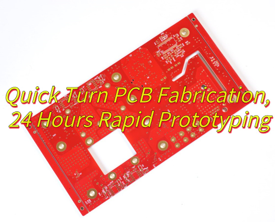
What is quick turn PCB fabrication? Let’s discover its technical spec, design strategies, production process, recommended manufacturer.

Are you worried about these issues?

  • Delays stalling R&D?
  • Low-cost quality risks?
  • Hidden costs inflating budgets?

Best Technology can provide service:

  • 48-hour full-cycle delivery.
  • 98%+ first board pass rate.
  • All-inclusive pricing.

Welcome to contact us if you have any request for quick turn PCB: sales@bestpcbs.com.

What Is Quick Turn PCB Fabrication?

Quick Turn PCB Fabrication is a highly efficient printed circuit board (PCB) production service. Through optimized processes, automated design checks, and synchronized production management, it completes the entire process from design to delivery within 24 hours to 5 days, significantly shortening product development cycles.

This service is designed to rapidly respond to the electronics industry’s needs for prototype verification and urgent production, allowing for flexible design adjustments. While the unit price is higher, it improves overall efficiency by saving time and costs. This service is widely used in consumer electronics prototypes (such as IoT devices), emergency medical and automotive parts, and rapid verification for startups.

Technical Specifications for Quick Turn PCB Fabrication

Parameter CategoryTechnical Specifications
Layer Count1-16 layers (standard)
18-32 layers (advanced)
Substrate TypesFR-4 (standard) / High-Tg FR-4 / Polyimide / PTFE (RF) / Aluminum-backed
Copper Thickness0.5oz(17ÎŒm)/1oz(35ÎŒm)/2oz(70ÎŒm)/3oz(105ÎŒm) (outer layers)
0.5oz-2oz (inner layers)
Min Trace/Space3mil(0.075mm)/4mil(0.1mm)/5mil(0.125mm) (standard)
2mil(0.05mm) (laser drilling)
Via TechnologyThrough-hole(PTH)/Blind(BVH)/Buried(BVH)
Microvia(≀0.15mm)
Surface FinishesHASL(Leaded/Lead-free)/ENIG/OSP/Immersion Silver/Immersion Tin
Solder Mask CoverageGreen(standard)/Blue/Red/White/Black/Clear (LPI)
Dimensional ToleranceBoard edges: ±0.15mm
Hole diameters: ±0.05mm
Outline: ±0.2mm (laser cutting)
Special ProcessesGold fingers/Carbon ink printing/Embedded resistors/Rigid-flex/Selective gold plating
Lead TimeSingle/double-sided: 24 hours
4-8 layers: 48-72 hours
10+ layers: 5-7 business days

How to Design Fast Turn PCBs to Reduce Production Cost?

1. Modular Pre-layout

  • Decompose complex circuits into independent functional modules (e.g., power modules, signal processing modules), develop standardized libraries for cross-project reuse. Universal power module packaging reduced layout time by 30%.

2. Structured Constraint Management

  • Import mechanical structure data (STEP format), define keep-out zones and height restrictions. Use 25mil sub-grid for critical components (BGA) and 50mil main grid for general layout to align with automated SMT machine precision.

3. Layer Count Dynamic Balancing

  • Determine minimum viable layer count through signal integrity simulation. Replace traditional through-holes with buried/blind via hybrid structures for high-speed signals. Reduced an 8-layer industrial control board to 6 layers, cutting costs by 18%.

4. Material Standardization Strategy

  • Prioritize FR-4 substrate, use localized PTFE hybrid construction for >5GHz signals. Develop enterprise material libraries with ≄70% standard component packages. Achieved 40% cost reduction compared to full Rogers 4350B solutions.

5. DFM Rules Embedded Design

  • Implement real-time DRC rules: minimum trace width/spacing 6mil, pad diameter via+12mil, solder mask opening trace+4mil. Reduced production defect rates from 2.3% to 0.7%.

6. Panelization Economic Design

  • Use V-cut + stamp hole hybrid panelization with 3mm process margin. Optimal panel count: 5pcs/panel, reducing unit costs by 35% versus single boards.

7. Concurrent Design Process

  • Execute parallel tasks during schematic phase: BOM standardization review, ECAD-MCAD mechanical interference checks, and FloTHERM thermal simulations. Shortened design cycles from 15 days to 9 days.
How to Design Fast Turn PCBs to Reduce Production Cost?

Double Sided PCB Quick Turn Fabrication Processes

1. Material Cutting

  • Substrate Preparation: Use automatic shearing machines to cut copper-clad laminates (FR-4/CEM-1) into standard sizes (e.g., 18″×24″) with edge tolerance ≀0.1mm.
  • Pre-Baking Treatment: Bake cut substrates at 120℃ for 2 hours to eliminate material stress and prevent warpage during subsequent processes.

2. Drilling

  • CNC Drilling: Employ 6-axis CNC drills with 0.2mm–3.2mm diameter bits, operating at 10,000–15,000rpm. Drilling time per panel ≀5 minutes.
  • Hole Cleaning: Immediately blow debris from holes using high-pressure air to avoid plating defects.

3. Electroless Copper Plating

  • Desmearing: Immerse drilled panels in potassium permanganate solution to remove resin residues from holes.
  • Copper Deposition: Deposit 0.3–0.5ÎŒm copper layer in alkaline solution for hole wall conductivity, taking ~45 minutes.

4. Circuit Imaging

  • Dry Film Lamination: Attach photosensitive dry film to substrates via thermal rollers at 110℃±5℃ and 1.5m/min speed.
  • Laser Exposure: Use LDI (Laser Direct Imaging) to project patterns onto dry film with ≀4mil resolution, eliminating film usage and saving 30% time.

5. Etching

  • Alkaline Etching: Immerse exposed panels in ammonium chloride-copper solution to remove non-conductive copper, maintaining line width tolerance ±0.05mm.
  • Quick Stripping: Rinse residual dry film with high-pressure water jet at 50℃±5℃ for ≀2 minutes.

6. Solder Mask Application

  • Screen Printing: Apply UV-curable solder mask using 36T mesh, achieving 20–30ÎŒm thickness with automatic alignment accuracy ±0.1mm.
  • Pre-Curing: Bake panels at 80℃ for 10 minutes in infrared tunnel oven to stabilize ink flow.

7. Surface Finish

  • Nickel deposition: 3–5ÎŒm thickness, 8–12 minutes
  • Gold deposition: 0.05–0.1ÎŒm thickness, 3–5 minutes
  • Alternative: HASL (Hot Air Solder Leveling) through tin furnace, taking ≀1 minute per panel.

8. Electrical Testing

  • Flying Probe Testing: Utilize 4-axis flying probe machines with 50–150g contact force. Single panel testing time ≀3 minutes, covering 100% networks.
  • Fault Marking: Automatically ink-mark short/open circuit locations for rework.

9. Routing & Depaneling

  • CNC Milling: Cut panels using 1mm diameter milling bits with ±0.05mm path accuracy. Single board routing time ≀2 minutes.
  • V-Cutting: For manual breakaway, score panels to 1/3 thickness at 30°–60° angle.

10. Final Inspection & Packaging

  • AOI Inspection: Scan solder pads/traces with 3D cameras to detect defects (e.g., solder balls, misalignment) at 1.2mÂČ/minute speed.
  • Vacuum Packaging: Seal panels in aluminum foil bags with desiccant, vacuuming to -0.1MPa for moisture/oxidation protection.
Double Sided PCB Quick Turn Fabrication Processes

Why Choose Best Technology as Quick Turn PCB Manufacturer?

Reasons why choose us as quick turn PCB manufacturer:

  • Ultra-Fast Delivery (24-72 Hours): Accelerates product development cycles by 50%+ compared to standard lead times, enabling rapid prototyping and market validation.
  • Advanced Technical Capabilities: Supports 1-16 layer boards with 0.1mm mechanical drilling and 0.1mm laser microvias. Minimum 3.5mil/4mil trace/space (1mil/1mil for HDI). Enables complex designs for IoT, wearables, and high-speed applications.
  • Automated DFM Checks: Reduces design errors by 30%+ through pre-production validation, minimizing rework costs.
  • Transparent Pricing Model: Eliminates hidden costs, with small-batch discounts for prototypes <50pcs.
  • 24/7 Engineering Support: Real-time technical assistance during design phase prevents costly production delays.
  • ISO-Certified Quality Control: Ensures reliability for medical/automotive applications with zero-defect tolerance.
  • Surface Finish Flexibility: HASL, ENIG, OSP options with 2ÎŒm gold thickness control.

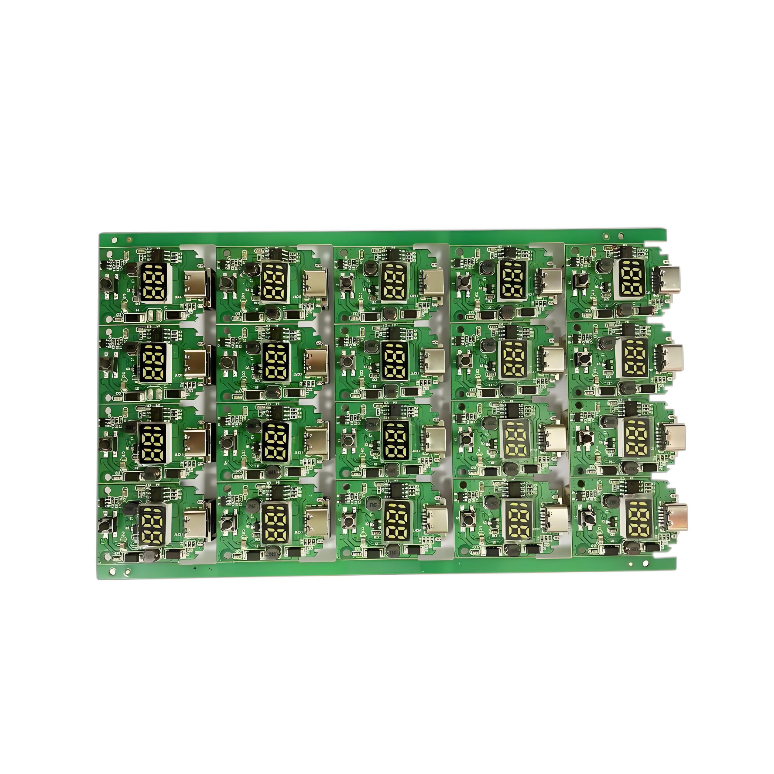
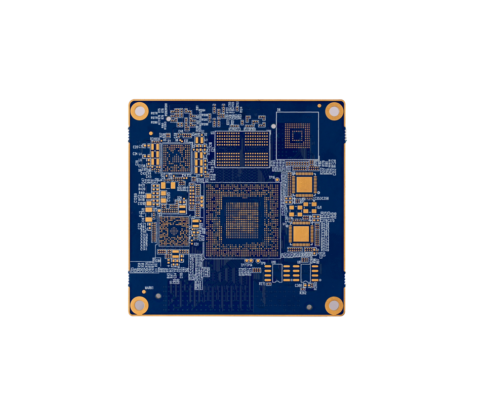
Below is a photo of FR4 PCB board we made before:

Why Choose Best Technology as Quick Turn PCB Manufacturer?

Our Quick Turn PCB Prototyping Time

LayersNormal ServiceFastest Service
17 Days24 H
28 Days24 H
410 Days48 H
610 Days72 H
812 Days72 H
≄10TBDTBD

Our Quick Turn PCB Options

1. Express Delivery (24-48 Hours)

  • Layer Support: 1-6 layers (standard boards).
  • Trace Width/Spacing: 3.5mil/4mil (1mil/1mil for advanced processes).
  • Drill Size: 0.2mm mechanical drilling (0.1mm laser microvias).
  • Suitable For: Urgent prototype verification, exhibition samples.

2. Standard Quick Turn Service (3-5 Days)

  • Layer Support: 8-10 layers (complex designs).
  • Material Options: FR-4, aluminum substrate, high-frequency materials (Rogers/PTFE).
  • Surface Finishes: HASL (leaded/lead-free), ENIG, OSP.
  • Suitable For: Small-batch trial production, functional testing.

3. Economy Quick Turn Solution (5-7 Days)

  • Copper Thickness: 0.5oz-3oz (standard options).
  • Solder Mask Colors: Green, Blue, Red, Black, White, Matte Black.
  • Cost Optimization: Volume discounts (50+ panels).
  • Suitable For: Pre-production validation, cost-sensitive projects.

How to Get A Quote for Quick Turn PCB Project?

Follow these steps to ensure accurate and efficient quotation:

1. Submit Design Files

  • Provide Gerber files (RS-274X format) or PCB design source files (Altium/Eagle/PADS).
  • Include assembly drawings if applicable.

2. Specify Technical Requirements

  • Layer count (1-16 layers).
  • Minimum trace width/spacing (e.g., 3.5mil/4mil).
  • Drill size requirements (mechanical/laser).
  • Material type (FR-4, aluminum, Rogers/PTFE).

3. Confirm Production Details

  • Order quantity (5-5,000+ pieces).
  • Surface finish preference (HASL/ENIG/OSP).
  • Copper thickness (0.5oz-6oz).
  • Solder mask color selection.

4. Indicate Special Requirements

  • Impedance control needs.
  • Blind/buried vias requirement.
  • High-frequency material certification.
  • RoHS compliance requirement.

5. Provide Contact Information

  • Company name and location.
  • Project timeline expectations.
  • Preferred communication channel (email/phone).

Welcome to contact us if you have any request for quick turn PCB: sales@bestpcbs.com.

Quick Turn PCB, Quick Turn PCB Prototype & Manufacturer
Tuesday, June 10th, 2025

Seeking for quick turn PCB solutions? This guide explores its definition, features, applications, 24-hour HDI prototyping techniques, welding defect prevention, manufacturer selection, cost optimization, and material customization.

Best Technology as a quick turn PCB prototype manufacturer, delivering urgent orders in 24 hours via automated production lines and laser-direct imaging for rapid precision. Our robust global supply chain ensures real-time access to high-demand materials like Rogers, minimizing delays. A 24/7 dedicated team provides instant DFM feedback and quote generation, accelerating time-to-market. Beyond speed, we support HDI, rigid-flex, and heavy copper designs with advanced quality checks (AOI, X-ray) and certifications (ISO 9001, IPC-A-600). With 98% on-time delivery and flexible scaling, we turn urgent needs into reliable solutions. Contact us for lightning-fast prototypes without compromising quality or innovation: sales@bestpcbs.com.

What Is Quick Turn PCB?

A quick turn PCB refers to a printed circuit board that is manufactured and delivered within an exceptionally short timeframe, typically ranging from 24 hours to a few days, by prioritizing rapid prototyping and streamlined production processes. This type of PCB focuses on accelerating design verification and testing cycles while maintaining essential quality standards to meet urgent project deadlines.

Quick Turn PCB

What Are Features of Quick Turn PCB?

Here are the features of quick turn PCB listed in detail:

  • Fast Production Time‌ – Typically completed within 24 hours to a few days, significantly quicker than standard PCB fabrication.
  • Expedited Processing‌ – Uses prioritized scheduling and streamlined workflows to minimize delays.
  • Flexible Order Quantities‌ – Supports both small-batch prototypes and low-volume production runs.
  • Advanced Manufacturing Techniques‌ – Incorporates high-speed drilling, laser direct imaging (LDI), and automated optical inspection (AOI) for efficiency.
  • Rapid Design Verification‌ – Enables quick testing and iteration of PCB designs before mass production.
  • On-Demand Services‌ – Allows urgent orders without long lead times, catering to time-sensitive projects.
  • High-Quality Standards‌ – Maintains reliability through strict quality checks despite the accelerated timeline.
  • Wide Material Compatibility‌ – Works with FR-4, high-frequency laminates, and flexible substrates.
  • Multi-Layer Support‌ – Capable of producing 2-layer to 16-layer (or more) boards in short timeframes.
  • Quick Turnaround for Revisions‌ – Facilitates fast design modifications and re-fabrication if needed.
Quick Turn PCB

What Are Applications of Quick Turn PCB?

Here are the major applications of quick turn PCBs:

  • Prototyping & Product Development‌ – Used for rapid iteration of electronic designs, allowing engineers to test and refine circuits quickly.
  • Consumer Electronics‌ – Supports fast-paced development cycles in smartphones, wearables, and smart home devices.
  • Automotive Electronics‌ – Helps in accelerating the testing of ADAS, infotainment systems, and EV components.
  • Medical Devices‌ – Enables quick prototyping of diagnostic equipment, wearable health monitors, and implantable devices.
  • Aerospace & Defense‌ – Facilitates urgent updates and testing of avionics, communication systems, and radar technologies.
  • Industrial Automation‌ – Used for developing control systems, sensors with short lead times.
  • Telecommunications‌ – Supports 5G infrastructure, RF modules, and networking hardware requiring rapid validation.
  • Research & Academia‌ – Allows universities and labs to quickly fabricate experimental circuits for academic projects.
  • Startups & Small Businesses‌ – Provides cost-effective, fast-turnaround solutions for limited-budget hardware projects.
  • Emergency Repairs & Replacements‌ – Helps in urgent PCB replacements for malfunctioning systems in critical operations.

How to Achieve 24-Hour Quick Turn Prototyping for HDI PCBs?

Below are methods about how to achieve quick turn prototype for HDI PCBs within 24 hours:

Instant Design Validation

  • Use an online DFM tool to auto-check Gerber/ODB++ files during quoting. Flag issues like trace/spacing errors or missing layers immediately.
  • Benefit: Fixes errors in minutes, avoiding 12+ hours of rework.

Pre-Stock Critical Materials

  • Keep local inventory of high-demand HDI materials (e.g., low-loss laminates, RCC for microvias). Partner with suppliers for 2-hour emergency deliveries.
  • Benefit: Eliminates delays from material shortages.

Dedicated High-Speed Line

  • Allocate a production line with 50kHz laser drills and LDI (Laser Direct Imaging) for 24-hour orders. Limit to 3–5 daily projects to maintain focus.
  • Benefit: Prioritized, error-free fabrication.

Parallel Processing

  • Split tasks: laser drill microvias while another team preps outer layers for AOI. Use LDI to skip film handling, saving 30% imaging time.
  • Benefit: Reduces total fabrication time by 40%.

Inline Inspections

  • Run AOI/AXI after drilling, plating, and etching. Auto-halt production if defects detected.
  • Benefit: Prevents failed final tests and rework.

Pre-Booked Express Shipping

  • Partner with overnight couriers (e.g., FedEx/DHL) for 10:30 AM next-day delivery. Include live tracking in client portals.
  • Benefit: Guaranteed deadline adherence.

Direct Engineer Access

  • Assign a dedicated engineer to each order. Provide WhatsApp/Slack for instant file tweaks or queries.
  • Benefit: Resolves issues in minutes, not hours.

Optional Fast-Track Testing

  • Skip final electrical tests for clients with DFM-compliant history. Offer as a “speed boost” option.
  • Benefit: Shaves 2–3 hours off lead time.

Post-Delivery Feedback

  • Send a 1-click survey: “Deadline met?” and “Reorder likelihood?” Use data to refine processes.
  • Benefit: Builds trust through accountability.
Quick Turn PCB Prototype

How to Avoid Welding Defects During Quick Turn PCB Prototyping?

Optimize Reflow Oven Profiles

    • Calibrate the reflow oven’s thermal profile to match the PCB’s specifications, including preheat, soak, reflow, and cooling stages. Use a data logger to validate temperature uniformity across the board.
    • Implementation: Adjust conveyor speed and zone temperatures in 5°C increments during testing to eliminate cold joints or solder beading.

    Implement Stencil Design Best Practices

      • Use laser-cut stainless-steel stencils with aperture sizes 1:1 to pad dimensions. For fine-pitch components (e.g., 0.3mm pitch QFPs), reduce aperture sizes by 10% to prevent solder bridging.
      • Implementation: Add solder paste release coatings to stencils and inspect paste deposition via automated SPI (Solder Paste Inspection) machines.

      Control Component Placement Accuracy

        • Ensure pick-and-place machines achieve ±25ÎŒm placement accuracy for 0201/01005 components. Use machine vision with fiducial markers to correct positional drift.
        • Implementation: Run a 5-point placement audit on the first article and adjust offsets before full production.

        Select Suitable Solder Paste

          • Choose Type 3 or Type 4 solder pastes (25–45ÎŒm particle size) for high-density boards. Prioritize no-clean fluxes with low residue to prevent ionic contamination.
          • Implementation: Store pastes at 2–10°C and allow 4-hour warm-up before use to eliminate slumping.

          Preheat PCBs to Reduce Thermal Shock

            • Precondition bare boards at 80–100°C for 30 minutes before soldering to drive off moisture and reduce warpage.
            • Implementation: Use infrared or convection preheaters integrated into the assembly line.

            Minimize Handling During Assembly

            • Avoid touching PCB surfaces with bare hands to prevent oil/residue transfer. Use ESD-safe vacuum grippers for component manipulation.
            • Implementation: Designate “no-touch” zones on the assembly line and enforce glove protocols.

            Validate First Article Inspection (FAI)

              • Perform 3D AOI (Automated Optical Inspection) after reflow to detect tombstoning, head-in-pillow, and solder shorts.
              • Implementation: Use multi-angle lighting and algorithms to differentiate true defects from cosmetic variations.

              Address Component Density Challenges

                • For BGAs and QFNs, use X-ray inspection to verify voiding (<25% void area) and fillet quality. Adjust reflow profiles if voids exceed limits.
                • Implementation: Deploy oblique-angle X-ray systems for better visibility under dense components.

                Maintain Equipment Calibration

                  • Verify stencil printers, pick-and-place machines, and reflow ovens quarterly using NIST-traceable standards.
                  • Implementation: Document calibration results in a centralized system for traceability.

                  Train Operators on Defect Recognition

                    • Conduct monthly sessions on visual inspection criteria (e.g., wetting angles, fillet heights) using microscope stations with annotated defect samples.
                    • Implementation: Use augmented reality tools to overlay acceptable/unacceptable solder joints during training.
                    Quick Turn Prototyp

                    How to Choose A Fast Turn Printed Circuit Board Manufacturer?

                    Below are methods about how to choose a quick turn PCB manufacturer:

                    Evaluate Technical Capabilities

                      • Verify the manufacturer’s ability to handle your design complexity (e.g., HDI, rigid-flex, or thick copper layers). Request a detailed capability sheet outlining minimum trace/space, via types, and material options.
                      • Action: Upload a sample Gerber file to test their DFM (Design for Manufacturability) analysis tool.

                      Assess Production Speed

                        • Request a breakdown of lead times for quoting, fabrication, and shipping. Confirm if they offer dedicated quick-turn lines with guaranteed 24-hour slots.
                        • Action: Compare quoted lead times against industry benchmarks (e.g., 5-day standard vs. 24-hour express).

                        Review Quality Control Processes

                          • Inquire about inline inspections (e.g., AOI, AXI) and final testing protocols (e.g., flying probe or electrical testing). Ask for defect rates (PPM) for recent projects.
                          • Action: Request sample inspection reports or certificates (e.g., IPC-A-600 compliance).

                          Check Material Inventory

                            • Ensure they stock high-demand substrates (e.g., FR-4, Rogers, or high-TG materials) and can source specialties (e.g., RF laminates) within 4 hours.
                            • Action: Ask for a list of pre-qualified suppliers to assess supply-chain reliability.

                            Validate Engineering Support

                              • Confirm availability of pre- and post-sales engineers for DFM feedback, stack-up advice, or last-minute design tweaks.
                              • Action: Test responsiveness by submitting a hypothetical design query and measuring reply time.

                              Compare Pricing Models

                                • Request quotes for both standard and express services. Look for transparency in surcharges (e.g., rush fees, NRE costs).
                                • Action: Use a cost-benefit analysis template to weigh speed vs. budget for your project.

                                Assess Order Tracking Systems

                                  • Ensure the manufacturer provides real-time updates via portal or API. Confirm visibility into fabrication milestones (e.g., drilling, plating, inspection).
                                  • Action: Test their tracking system with a dummy order to evaluate usability.

                                  Review Customer Feedback

                                    • Check third-party platforms (e.g., Trustpilot) for reviews on reliability, communication, and defect rates. Prioritize manufacturers with ≄4.5-star ratings.
                                    • Action: Contact references to ask about on-time delivery and post-sales support.

                                    Confirm Flexibility for Revisions

                                      • Inquire about policies for ECOs (Engineering Change Orders) during production. Ensure minimal fees for minor tweaks (e.g., via size adjustments).
                                      • Action: Submit a sample ECO to gauge approval speed and cost impact.

                                      How to Reduce the Production Cost of Quick Turn PCB without Compromising Quality?

                                      Simplify Design Complexity

                                        • Reduce unnecessary layers or via types (e.g., replace blind vias with through-hole vias where feasible). Use design rules checker (DRC) tools to identify over-engineered traces or spacing.
                                        • Action: Share design guidelines with clients to balance performance and cost.

                                        Optimize Panel Utilization

                                          • Maximize PCB density per panel using automated nesting software. Combine multiple small boards into a single array with V-scoring.
                                          • Action: Calculate panel efficiency (e.g., 85%+ utilization) before production.

                                          Standardize Material Selection

                                            • Use cost-effective substrates (e.g., FR-4) instead of specialty materials (e.g., Rogers) unless RF performance is critical. Maintain a list of pre-qualified, low-cost laminates.
                                            • Action: Offer material swaps with minimal impact on electrical performance.

                                            Automate Fabrication Steps

                                              • Invest in laser direct imaging (LDI) to eliminate film costs and reduce setup time. Use automated optical shaping (AOS) for faster solder mask application.
                                              • Action: Compare labor hours pre- and post-automation to quantify savings.

                                              Implement Lean Inventory

                                                • Adopt a just-in-time (JIT) system for materials like solder paste and dry film. Partner with suppliers for 24-hour replenishment to reduce storage costs.
                                                • Action: Track inventory turnover rates and aim for ≀7 days of stock.

                                                Streamline Testing Protocols

                                                  • Replace 100% electrical testing with flying probe tests for low-volume runs. Use boundary scan (JTAG) for complex boards to reduce fixturing costs.
                                                  • Action: Validate test coverage via sample boards to ensure defects are caught.

                                                  Reuse Engineering Data

                                                    • Archive and repurpose drilling programs, impedance profiles, and stack-up designs for repeat clients. Avoid redundant setup fees.
                                                    • Action: Implement a cloud-based library for client-specific engineering data.

                                                    Negotiate Volume Discounts

                                                      • Bundle quick-turn orders with recurring clients to hit supplier volume tiers. For example, negotiate 5% off solder paste for monthly orders ≄50kg.
                                                      • Action: Share aggregated forecasts with suppliers for better pricing.

                                                      Reduce Scrap Through Process Controls

                                                        • Use statistical process control (SPC) to monitor etching, plating, and drilling. Address out-of-spec parameters (e.g., line width deviation) in real time.
                                                        • Action: Aim for ≀0.5% scrap rate through proactive adjustments.

                                                        Outsource Non-Core Processes

                                                          • Partner with specialized vendors for secondary operations (e.g., conformal coating, conformal coating, or selective soldering). Avoid capital investments in low-utilization equipment.
                                                          • Action: Audit subcontractors’ quality systems to maintain standards.

                                                          Leverage Regional Labor Arbitrage

                                                            • Establish facilities in regions with lower operating costs while maintaining local sales/support teams. Use ERP systems to bridge time-zone gaps.
                                                            • Action: Compare total cost of ownership (TCO) across locations.

                                                            Educate Clients on Cost Drivers

                                                              • Provide clients with a “cost impact” dashboard showing how design choices (e.g., gold fingers, 1oz vs. 0.5oz copper) affect pricing.
                                                              • Action: Offer design-for-cost (DFC) workshops to align priorities.

                                                              Can You Customize Special Substrate Material For Quick Turn PCB?

                                                              Yes, Best Technology offers tailored substrate material solutions for quick turn PCBs, including specialized laminates like high-frequency Rogers, ceramic-filled PTFE, or flexible polyimide. Additionally, we provide customizable surface finishes such as immersion tin, immersion silver, and ENEPIG to meet unique application requirements. Customizing substrates and finishes enables clients to align PCBs with precise performance needs—such as low-loss dielectric for 5G modules, high-thermal-conductivity materials for power electronics, or biocompatible finishes for medical devices. By pre-vetting materials through rigorous DFM (Design for Manufacturability) reviews, we eliminate compatibility risks and reduce iteration cycles. For instance, switching from ENEPIG to ENIG for non-bonding areas can cut costs by 20% without sacrificing reliability. Our 24-hour prototype service allows clients to validate designs with custom specs before scaling production, ensuring seamless integration with downstream processes. This approach balances speed, cost, and performance, empowering clients to innovate faster than competitors relying on generic solutions.