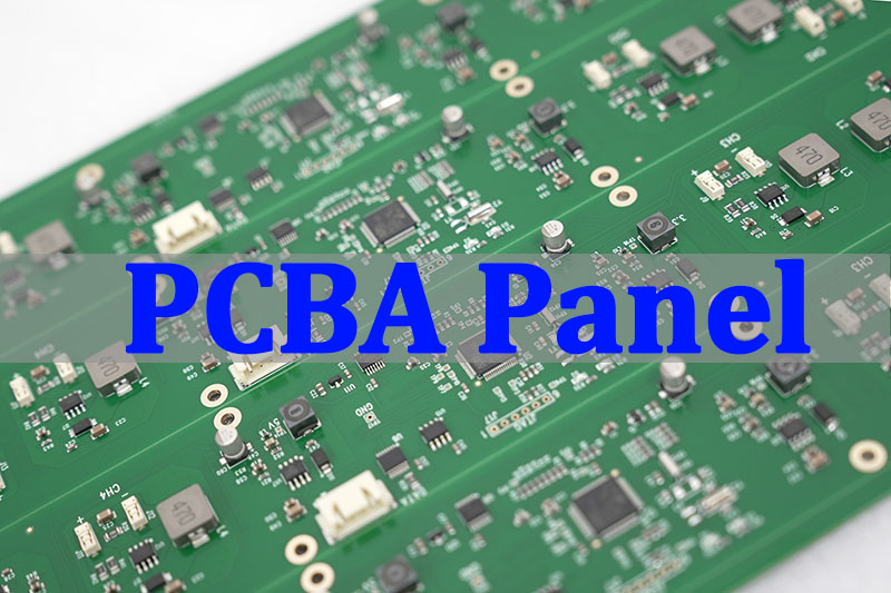
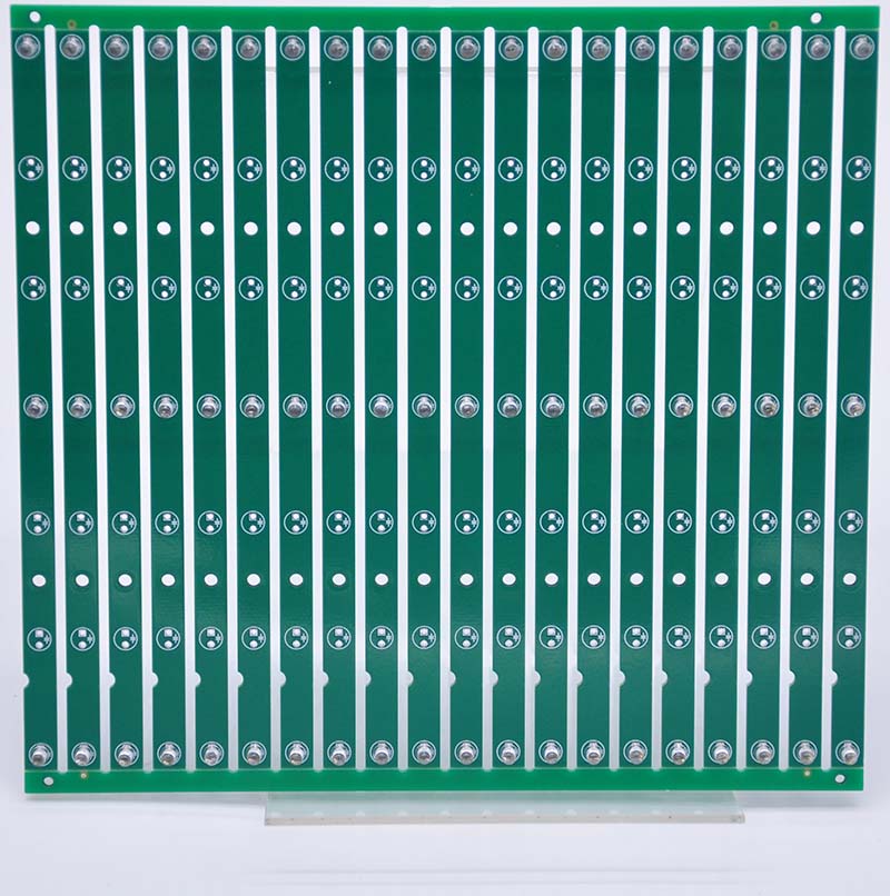
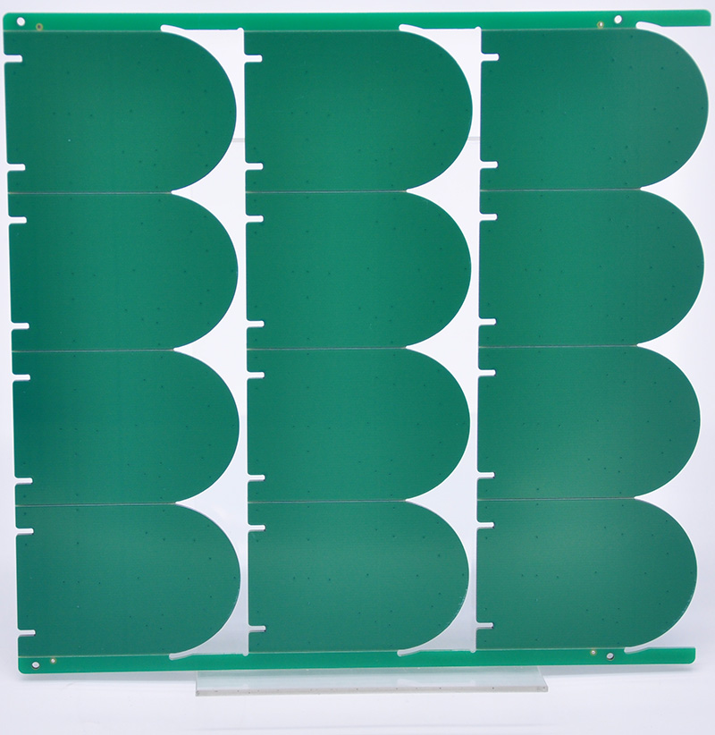
A PCBA panel, or printed circuit board assembly panel, is a larger board that holds multiple identical or different PCB units for streamlined manufacturing. This article will explore optimized panel strategies to maximize reliability, yield, and cost-effectiveness in high-volume production, covering design guidelines, common mistakes, and efficiency calculations.
What are the most common pain points in PCB panelization?
- Assembly errors: Misalignment and solder defects caused by poor panel design.
- Low utilization: Board material wasted due to inefficient panel layouts.
- Process inefficiency: Excessive manual handling slows down production.
- Stress and breakage: Improper depaneling leads to bent boards or cracked parts.
- Cost overruns: Yield loss and rework inflate the real panel cost.
Addressing these challenges requires a systematic approach. Here are five key solutions from a seasoned PCBA manufacturer’s perspective:
- DFM-driven panel design: Apply clear panelization guidelines early with your manufacturer.
- Utilization optimization: Maximize panel fill before fabrication.
- Automation-ready panels: Design for SMT, testing, and depaneling automation.
- Controlled breakaway methods: Use appropriate V-scoring or tab routing with stress relief.
- Total cost evaluation: Optimize for yield and throughput, not panel price alone.
As a professional PCBA manufacturer with 20 years of experience in high-mix, high-volume production, EBest Circuit (Best Technology) partners with clients from the design stage to implement optimized PCBA panel strategies. Our engineering team leverages advanced software and proven PCB panel design principles to ensure maximum reliability and efficiency for your mass production runs. For a consultation on your next PCB assembly project, pls feel free to contact us at sales@bestpcbs.com.

What Is a PCBA Panel and Why It Matters in Mass Production?
A PCBA panel is a carrier board that combines multiple individual PCBs into a single unit for efficient assembly and testing.
- Single-unit processing: Multiple PCBs are assembled together through SMT, wave soldering, and testing.
- Higher throughput: Panelization allows many boards to be populated and soldered simultaneously.
- Mechanical stability: Small or irregular boards remain stable during automated handling.
- Reduced handling risk: Fewer manual steps lower the chance of damage and human error.
- Process standardization: Consistent panel formats improve repeatability and quality control.
- Cost and scale enablement: Optimized panels support mass production with predictable cost and output.

What PCB Panelization Methods Are Used in Modern PCBA Lines?
PCB panelization is the technique of arranging multiple board designs onto a single panel. The choice of method directly impacts assembly ease, depaneling quality, and board integrity. Modern lines primarily use three methods, often in combination.
- Tab Routing (Mouse Bites): Individual boards are connected by small, perforated tabs. This method is ideal for complex board shapes or when components are placed very close to the edge.
- V-Scoring (V-Grooving): A V-shaped groove is cut partially through the panel material, leaving a thin web of material to hold boards together. It allows for very fast, clean depaneling with specialized equipment.
- Mixed Panelization: Combines V-scoring for straight edges and tab routing for complex contours within the same PCB panel array.
The table below summarizes the key differences:
| Method | Best For | Depaneling | Edge Quality |
|---|---|---|---|
| Tab Routing | Irregular shapes, edge components | Break by hand or machine; slower | Requires smoothing (nubs remain) |
| V-Scoring | Rectangular/regular shapes, high speed | Fast snap or machine separation | Very clean, straight edges |
| Mixed | Complex panels with mixed requirements | Combination of methods | Varies by edge type |
Choosing the right method depends on your board’s geometry, component placement, and available depaneling equipment at the factory.
How Are PCB Panel Sizes Determined for Different Board Designs?
Determining the optimal PCB panel sizes is a balancing act between machine compatibility, material utilization, and assembly efficiency. It’s not a one-size-fits-all calculation. Key factors include:
- Equipment Constraints: The panel must fit within the minimum and maximum dimensions of SMT pick-and-place machines, reflow ovens, wave solder carriers, and testing fixtures. Standard panel sizes often align with common equipment specs (e.g., 330mm x 250mm).
- Material Utilization: The primary goal is to fit as many units as possible with minimal waste. This is where a PCB panel utilization calculator becomes invaluable.
Utilization (%) = (Total area of individual boards / Total panel area) x 100.
Aim for >80% utilization where possible. - Board Shape and Array: The shape of your single PCB dictates how it can be nested or arrayed on the panel. Rectangular boards tile efficiently, while odd shapes may require a PCB panel array with rotation or different orientations to fill space.
- Process Requirements: Space must be allocated for tooling holes (for machine alignment), fiducial marks, test coupons, and breakaway tabs or V-score channels.
- Handling and Depaneling: Very large panels may be difficult to handle or may warp in reflow; very small or thin panels may lack rigidity. The size must allow for safe, reliable depaneling.
In practice, manufacturers like Best Technology use software to simulate different layouts and calculate PCB panel configurations that deliver the best compromise of all these factors for your specific design.
What Is a PCB Panel Array and How Does It Improve Assembly Efficiency?
A PCB panel array refers to the specific arrangement or matrix of individual PCB copies on the panel. It is the heart of assembly optimization. A well-planned array improves efficiency in several concrete ways:
- Maximized Throughput: By populating 10, 20, or even 50 boards in one machine cycle, the effective placement rate of components is multiplied.
- Reduced Setup Time: Programming and calibrating machines for one panel is vastly faster than for hundreds of individual boards.
- Consistent Quality: All boards on a panel experience identical process conditions (solder paste application, reflow profile, wave solder exposure), minimizing unit-to-unit variation.
- Streamlined Testing: Automated test systems (like flying probe or fixture-based testers) can sequence through all boards on a panel with minimal movement, speeding up validation.
- Optimized Material Flow: Handling, storing, and moving panels is logistically simpler than managing loose boards, reducing risk of damage and mix-ups.
For example, a 2×5 array processes ten boards at once, effectively making the assembly line ten times faster for the placement and soldering stages compared to single-board processing. This multiplicative effect is why panel array design is critical for cost-effective mass production.
How Do PCB Panelization Guidelines Affect Yield and Cost Control?
Adhering to robust PCB panelization guidelines is a direct lever for controlling yield and cost. These guidelines standardize the process to prevent defects and waste.
Key Panel Design Guidelines:
- Clearance & Spacing: Maintain sufficient spacing between board edges (typically 3mm minimum) and from components to panel borders/scores (2mm minimum) to prevent interference during assembly and depaneling.
- Tooling & Fiducials: Include standardized, unplated tooling holes and global/fine-pitch fiducial marks for precise machine alignment across the entire panel.
- Depaneling Considerations: Design breakaway tabs with proper size (e.g., 5mm x 5mm) and spacing. For V-scoring, ensure components are kept away from the score line.
- Panel Strength: Ensure the panel frame is rigid enough to prevent warping or sagging during high-temperature reflow soldering. This may require strategic tab placement or a thicker panel core.
- Waste Strips: Include waste strips on at least two opposing sides to provide edge grip for conveyor systems and space for process coupons.
Ignoring these guidelines can lead to misprinted solder paste, misaligned components, cracked solder joints during depaneling, and panel warpage—all of which directly scrap boards and increase cost per functional unit. A disciplined approach to panelization is a non-negotiable aspect of reliable mass production.
What Factors Influence PCB Panel Price in Production Runs?
While the unit PCB panel price is part of the total cost, it’s influenced by several interconnected factors that savvy buyers should understand:
- Panel Size and Material: Larger panels use more base material (FR-4, Rogers, etc.), directly increasing cost. The choice of material itself is a major cost driver.
- Number of Layers: A multilayer PCB panel board is more expensive to fabricate than a double-sided one due to increased lamination and drilling steps.
- Panel Utilization: Low utilization means you are paying for wasted material. A higher utilization percentage achieved through smart PCB panel design lowers the effective cost per individual board.
- Special Processes: Additional requirements like controlled impedance, gold plating, blind/buried vias, or heavy copper increase the fabrication complexity and cost of the panel.
- Order Quantity: Economies of scale apply. The cost per panel decreases with higher volume runs, as setup and tooling costs are amortized over more units.
Understanding this breakdown helps in making informed trade-offs. For instance, a slightly larger panel with higher utilization might yield a lower cost per final assembled board than a smaller, inefficient panel.
What Common PCB Panelization Mistakes Lead to Assembly or Yield Issues?
Even experienced teams can stumble on panelization. Here are common pitfalls and how to avoid them:
- Ignoring Machine Capabilities: Designing a panel larger than the printer or pick-and-place machine can handle leads to immediate production stoppage.
- Insufficient Clearance: Placing components or traces too close to routing paths or V-score lines guarantees damage during depaneling.
- Weak Panel Frame: A flimsy frame can cause the panel to warp in reflow oven, leading to poor soldering and making automated depaneling impossible.
- Missing Fiducials: Without proper fiducials, especially for fine-pitch components, placement accuracy suffers, causing shorts or open circuits.
- Poor Tab Design: Too few or weak tabs can cause boards to detach during processing; too many or poorly positioned tabs make depaneling difficult and stressful for the boards.
- Overlooking Test Access: Failing to provide space or clearance for in-circuit test (ICT) probes or fixtures on the panel can make electrical testing cumbersome or impossible.
The remedy is always early collaboration and a formal DFM check with your PCBA manufacturer before panel design is finalized.
How Should PCB Panel Design Be Optimized for PCBA Assembly?
Optimizing PCB panel design requires a holistic view of the entire assembly and test process. Follow these principles:
- Optimize for SMT Assembly: Ensure the panel is rigid, flat, and has reliable fiducials. Orient all boards in the same direction on the panel to minimize pick-and-place head rotation and maximize speed.
- Facilitate Soldering: Consider thermal mass distribution. A panel with a very dense area next to a sparse area may solder unevenly. Balance the layout if possible.
- Integrate Testing Strategy: Design the panel to accommodate your test method. Include test points accessible in the panelized form or design it for easy break-in before testing if needed.
- Plan for Depaneling: Choose the breakaway method (V-score vs. tabs) early in the layout process and design the board outlines accordingly. Provide clear, clean break lines.
- Maximize Real-Estate: Use every available millimeter wisely. Nest different board designs together (if volume allows) or adjust the board outline slightly to improve utilization without affecting functionality.
- Standardize Where Possible: Using consistent panel sizes and tooling hole patterns across multiple projects can reduce factory setup time and cost for your products.
By addressing these areas, you create a panel that is not just a carrier, but an active tool for manufacturing excellence.

To conclude, a PCBA panel is the strategic backbone of efficient electronics manufacturing, enabling the simultaneous processing of multiple boards to achieve scale, consistency, and cost control. This article has outlined the core strategies—from selecting the right PCB panelization method and optimizing PCB panel sizes with a PCB panel calculator, to avoiding costly design mistakes—that are essential for reliable mass production.
With in-house PCB and PCBA manufacturing, EBest Circuit (Best Technology) has 20 years of proven experience serving Medical, Industrial Control, Robotics, and IoT PCBA projects. Backed by 1,000+ supply-chain partners, we deliver assured quality and on-time production. Pls feel free to reach out to our engineering and sales team anytime at sales@bestpcbs.com for a detailed consultation.
FAQs about PCBA Panel
What Is the Purpose of a PCBA Panel in Assembly?
A PCBA panel groups multiple individual PCBs into a single carrier to improve assembly efficiency, handling stability, and consistency during SMT, soldering, and testing.
When Should a Project Use a Custom PCBA Panel Instead of Single Boards?
A custom PCBA panel is recommended for small boards, irregular shapes, or mass production, where automation, throughput, and cost control are critical.
What Is the Difference Between a PCBA Panel and a Single PCB?
A PCBA panel contains multiple individual PCBs processed together, while a single PCB is assembled and handled one board at a time, resulting in lower efficiency and higher handling risk.
Does PCBA Panelization Affect Testing and Inspection?
Yes. A well-designed PCBA panel allows inline testing, AOI, and functional testing to be performed more efficiently before depaneling, improving overall test consistency.
Who Should Define the PCBA Panel Design—The Designer or the Manufacturer?
PCBA panel design is best finalized collaboratively. Designers define functional requirements, while manufacturers optimize panel layout for assembly, depaneling, and yield.


