PCB manufacturing PCB manufacturing
Home > Blog

Posts Tagged ‘pcb stencil thickness’

What Is a Circuit Board Stencil? PCB Stencil Material
Monday, January 26th, 2026

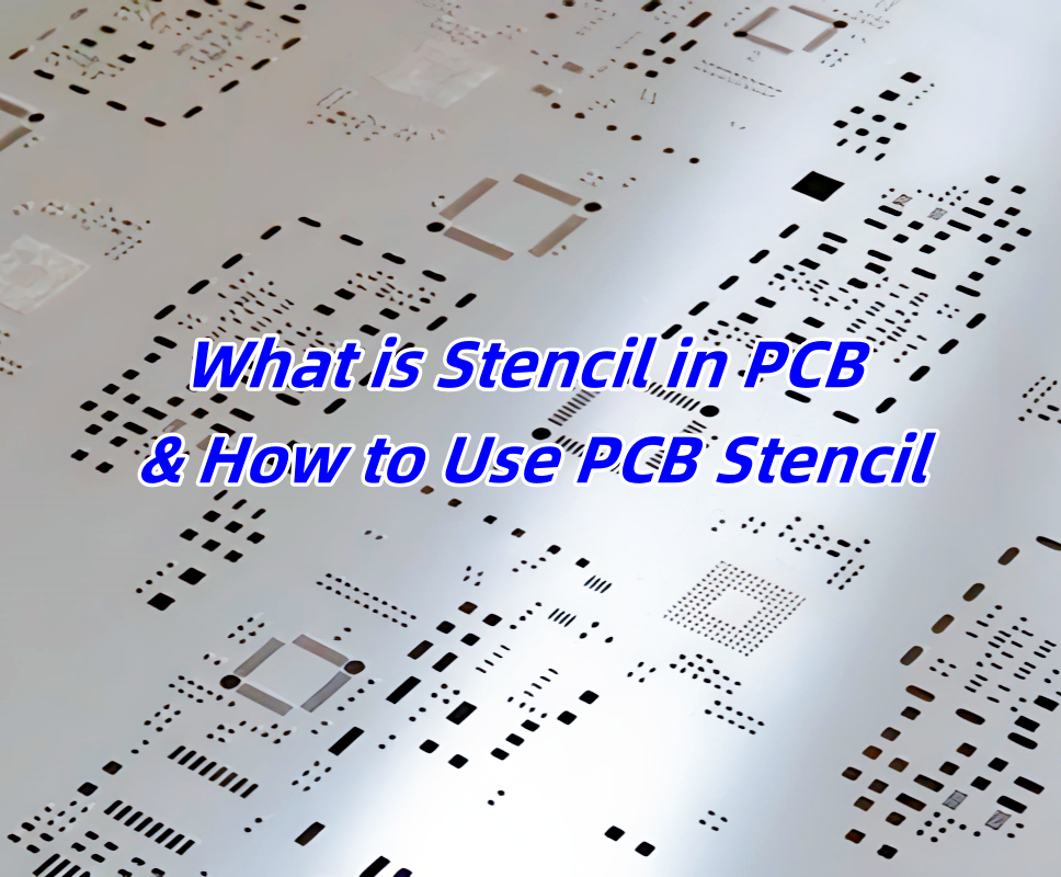
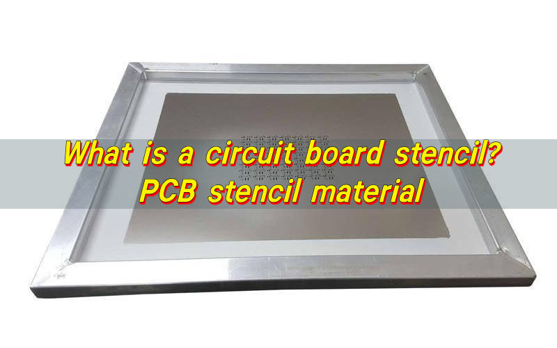
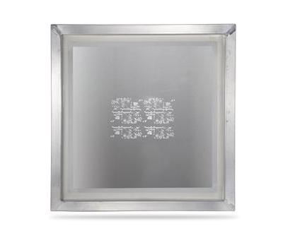
Circuit board stencil — also called a PCB stencil or SMT stencil—is a thin sheet with laser-cut openings that align with the solder pads on a printed circuit board. During surface-mount assembly, solder paste is swept across the stencil so precise, repeatable amounts are deposited only where components will be placed.

What Is a Circuit Board Stencil? PCB Stencil Material

What Is a Stencil Mask in PCB?

Stencil mask in PCB assembly is a thin sheet with precisely cut openings that match the solder pad layout of the board. During SMT production, solder paste is applied through these openings onto the pads before component placement.

Stencil circuit board defines where solder paste goes and, just as importantly, where it does not. Without a stencil, paste deposition would rely on manual methods or uncontrolled dispensing.

Printed circuit board stencils are used in nearly all automated SMT lines because they support repeatability. Once aligned, the same stencil can be used for hundreds or thousands of print cycles with minimal variation.

In manufacturing environments like EBest Circuit (Best Technology), stencil data is reviewed together with Gerber files during DFM checks. This coordination ensures the stencil design supports the real assembly conditions rather than simply matching the PCB layout on paper.

What Material Is Used for PCB Stencils?

The most common PCB stencil material is stainless steel, chosen for its durability, flatness, and resistance to corrosion. Stainless steel stencils can maintain sharp aperture edges over many print cycles, which helps deliver consistent solder paste release.

Within stainless steel options, there are two main surface conditions. Standard stainless steel offers reliable performance for general applications. Polished or nano-coated steel improves paste release, especially for small apertures and fine-pitch components.

Nickel stencils provide smoother walls and are sometimes used for ultra-fine features. Polymer or Mylar stencils are used mainly for low-volume prototyping, where cost and speed matter more than longevity.

From a production standpoint, stainless steel remains the default choice for professional assembly. At EBest Circuit (Best Technology), stainless steel stencils are standard for customer projects because they balance print quality, lifespan, and cost efficiency across both prototype and mass production runs.

What Are the Different Types of Stencils?

Circuit board stencils can be classified by structure and usage method. Each type serves a specific production scenario.

Common stencil types include:

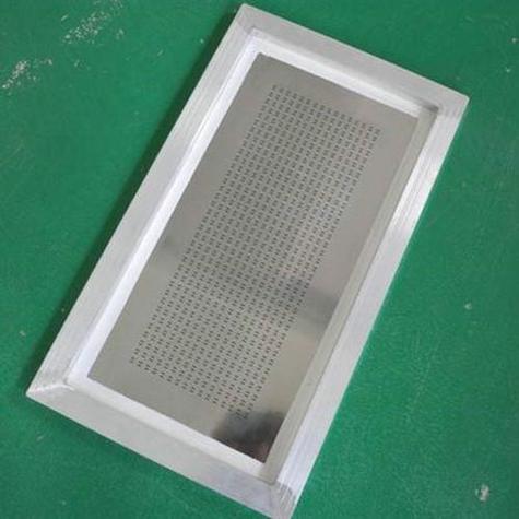
  • Framed stencils, which are permanently mounted in a rigid aluminum frame. These are ideal for high-volume SMT lines because they maintain flatness and alignment over repeated use.
  • Frameless stencils, also known as foil stencils. These are tensioned in a reusable frame system and are popular for flexible production environments.
  • Prototype stencils, usually smaller and sometimes made from polymer materials. These support quick setup for early design validation.
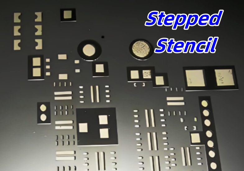
  • Step stencils, which have varying thicknesses in different areas to accommodate mixed component sizes on the same board.

The choice of stencil type depends on production volume, board size, and process stability requirements. For example, a framed stencil offers excellent consistency in mass production, while a frameless stencil provides faster changeover in multi-project lines.

What Is a Circuit Board Stencil? PCB Stencil Material

EBest Circuit (Best Technology) frequently recommends frameless stencils for low-to-medium volume projects because they reduce storage costs and allow faster adjustments without compromising print quality.

What Is a PCB Stencil Made Of?

At its core, a PCB stencil is made of a flat metal sheet with laser-cut apertures. Stainless steel is the dominant base material, but what differentiates stencils is not just the metal itself.

Laser cutting is the preferred method for modern stencils. It produces clean aperture edges and tight tolerances, which directly affect paste release. After cutting, stencils may undergo electro-polishing to smooth the aperture walls.

Some stencils include surface coatings. Nano-coatings reduce paste adhesion, making cleaning easier and extending the time between maintenance cycles. While coatings add cost, they often pay for themselves in reduced downtime and improved consistency.

In professional assembly operations, stencil selection is treated as part of the overall process design. At EBest Circuit (Best Technology), stencil specifications are aligned with solder paste type, squeegee parameters, and reflow profiles to create a balanced, predictable system.

How to Make PCB Stencil?

Creating a circuit board stencil starts with accurate PCB design data. The stencil is derived directly from the solder paste layer in the design files, not from the copper layer.

The typical stencil fabrication process includes several steps:

  • Extracting the paste layer from the PCB design files.
  • Adjusting aperture sizes to match component needs.
  • Laser cutting the apertures into the stencil material.
  • Polishing or coating the stencil surface if required.
  • Inspecting the stencil for flatness and dimensional accuracy.

At EBest Circuit (Best Technology), stencil design is reviewed as part of the PCBA preparation stage. This review ensures that stencil data reflects real assembly conditions rather than relying solely on default design outputs.

How to Cover Up Holes in a Stencil Circuit Boards?

Sometimes, certain pads or vias should not receive solder paste. In these cases, covering or blocking stencil openings becomes necessary.

Several practical methods are used:

  • Modifying the stencil design to remove specific apertures.
  • Applying stencil tape to temporarily block openings.
  • Using removable masks designed for repeated use.

Design-level solutions are preferred whenever possible because they eliminate manual intervention. Temporary blocking methods are useful during prototyping or when accommodating last-minute changes.

In controlled production environments, EBest Circuit (Best Technology) typically addresses these needs at the design stage. This approach reduces operator error and maintains consistency across production batches.

What Is a Circuit Board Stencil? PCB Stencil Material

How Thick Should a PCB Stencil Be?

PCB stencil thickness directly influences solder paste volume. Choosing the right thickness is one of the most critical stencil decisions because it affects both solder joint quality and defect rates.

Common stencil thickness values include 0.10 mm, 0.12 mm, and 0.15 mm. Thinner stencils are used for fine-pitch components, while thicker stencils support larger components and connectors.

Thickness selection depends on several factors:

  • Smallest component pitch on the board.
  • Pad size and shape.
  • Solder paste type.
  • Target production yield.

In mixed-technology boards, step stencils are often used to balance competing requirements. EBest Circuit (Best Technology) frequently recommends step stencils for boards combining fine-pitch ICs with large power components.

How to Choose the Correct Stencil?

Choosing the correct stencil requires a holistic view of the assembly process. It is not just about matching pad layouts but about supporting stable printing under real conditions.

Key considerations include:

  • Board complexity and component mix.
  • Production volume and changeover frequency.
  • Cleaning and maintenance capabilities.
  • Cost versus lifespan expectations.

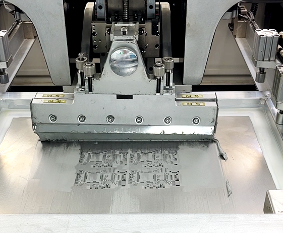
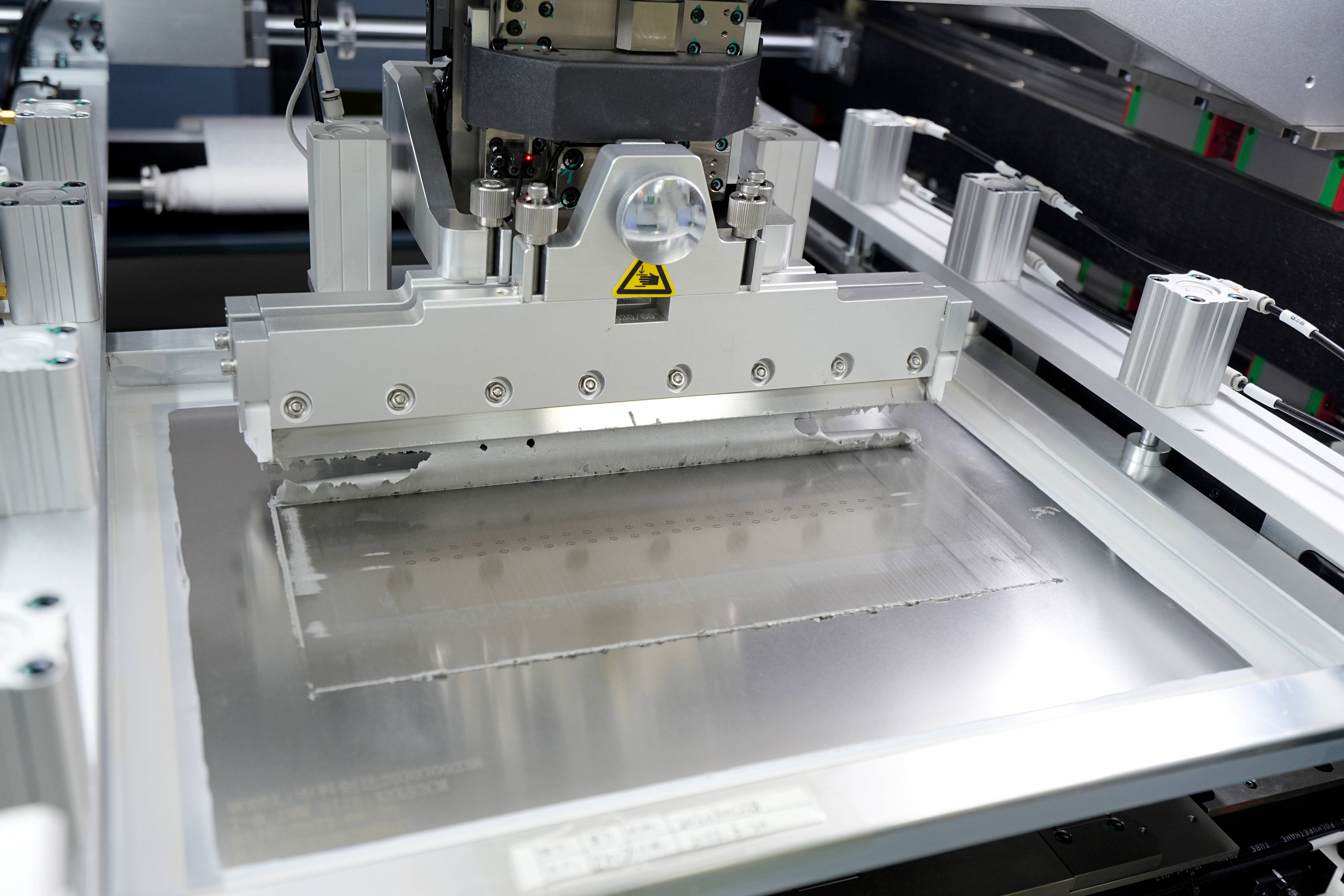
How to Use PCB Stencil?

Using a PCB stencil correctly involves careful setup, alignment, and process control. The typical usage process includes:

  • Securing the PCB in the printing fixture.
  • Aligning the stencil apertures with the PCB pads.
  • Applying solder paste evenly across the stencil.
  • Using a controlled squeegee stroke to print the paste.
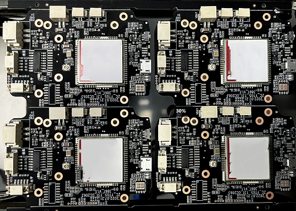
  • Inspecting the paste deposits before component placement.

Squeegee speed, pressure, and angle should remain stable throughout production. Regular cleaning prevents paste buildup that can distort print quality.

At EBest Circuit (Best Technology), stencil printing is treated as a controlled process step. Operators follow standardized parameters, and SPI inspection is used to verify paste quality before placement begins.

What Is a Circuit Board Stencil? PCB Stencil Material

Conclusion:

Circuit board stencil is more than a simple metal sheet. It is a precision tool that directly affects solder quality, assembly yield, and long-term reliability.

If you would like guidance on stencil selection, PCB fabrication, or turnkey PCBA services, contact sales@bestpcbs.com for professional support tailored to your project requirements.

PCB Stencil: What is Stencil in PCB & How to Use PCB Stencil
Tuesday, February 18th, 2025

What is a Stencil in PCB?

A PCB stencil is a precision tool used in the process of assembling printed circuit boards. Its main function is to apply solder paste to the board in a controlled manner, ensuring the paste only reaches the pads where components will be mounted. By creating uniform paste deposits, the stencil facilitates the correct soldering of components during the assembly process, contributing significantly to the quality and reliability of the final product.

PCB Stencil: What is Stencil in PCB & How to Use PCB Stencil

What Does a Stencil Do?

A PCB stencil plays several crucial roles in the PCB assembly process, including:

1. Applies Solder Paste: The primary function of a stencil is to accurately apply solder paste to the PCB. The paste is deposited onto the pads of the PCB through the openings in the stencil, ensuring the right amount of paste is used for each component.

2. Improve Precision: By using a stencil, manufacturers can achieve highly precise solder paste placement. This is especially important for fine-pitch components, where precision is key to avoiding defects like bridging or insufficient solder.

3. High Efficiency: Stencils speed up the solder paste application process, making it more efficient than manual paste application. This is particularly beneficial in high-volume manufacturing, where consistency and speed are vital.

4. Reduces Human Error: Using a stencil minimizes the chances of human error in solder paste application. This leads to more consistent and reliable results, reducing the likelihood of defects in the final product.

5. Facilitates High-Volume Production: Stencils are essential for mass production, allowing manufacturers to quickly and efficiently apply paste across multiple PCBs with high consistency.

6. Improves Reflow Soldering: With the right amount of solder paste applied, the stencil helps ensure that the reflow soldering process is carried out effectively, leading to strong and durable solder joints.

What is a PCB Stencil Consist of?

A PCB stencil consists of several crucial components that work together to ensure precise solder paste application. These elements include:

1. Frame

The frame is essential for holding the stencil in place during the application process. It is categorized into movable frames and fixed frames. The movable frame attaches the steel plate directly to the frame, allowing the template to be reused. On the other hand, the fixed frame uses adhesive to attach the wire mesh to the formwork. For optimal performance, a strong frame with uniform steel tension—typically between 35 and 48 N/cm²—is preferred. The normal fixed frame tension is between 35 N to 42 N, ensuring stability and accuracy.

2. Sheet Plates

High-quality stainless steel plates such as 301/304 stainless steel are commonly used because they offer excellent mechanical properties, significantly increasing the service life of the stencil. Other materials such as copper plates, nickel alloy, and polyester may also be used, depending on the specific application requirements.

3. Mesh

The mesh is used to fix the steel plates and formwork in place. There are two main types of mesh: stainless steel mesh and polymer polyester mesh. Stainless steel mesh is typically around 100 mesh and ensures stable tension, but it can deform and lose tension over time. Polyester mesh, on the other hand, is made from an organic fabric that doesn’t easily deform and has a longer service life, making it a more durable option for long-term use.

4. Adhesive (Glue)

The glue used in PCB stencils serves as the binding material that attaches the trellis frame to the steel sheet. It is an essential part of maintaining the integrity and stability of the stencil. The adhesive used needs to provide strong adhesion and be able to withstand heavy cleaning with various plate cleaners without losing its effectiveness.

Together, these components—frame, sheet, mesh, and glue—combine to form a PCB stencil that ensures accurate, consistent, and efficient solder paste application during the PCB assembly process.

What Are the Different Types of Stencils?

There are various types of PCB stencils, each designed for specific applications and production requirements:

  • Laser-Cut Stencils: These are the most accurate and commonly used type. Laser cutting provides high precision, making these stencils perfect for fine-pitch components or designs with intricate details.
  • Etched Stencils: Etching is an older method but still used for simpler projects. Though less precise than laser-cut stencils, etched stencils are still valuable for projects where absolute precision is not as critical.
  • 3D Printed Stencils: 3D printing technology has opened up a new avenue for creating PCB stencils. This method is ideal for low-volume or prototype PCB assembly, offering flexibility and faster turnaround times for custom designs.
  • DIY Stencils: For hobbyists or small-scale production, DIY methods using materials like adhesive-backed foil or plastic sheets can be used to create simple stencils. These are cost-effective but come with trade-offs in precision and durability.
  • Stepped Stencil: A stepped stencil features varying thicknesses across different areas of the stencil. These thickness changes, or “steps,” allow the stencil to deposit different amounts of solder paste for different components on the same PCB. Stepped stencils are particularly useful when there is a mix of fine-pitch components and larger, more spaced-out components on the same board. Below is a typical photo of stepped stencil.
PCB Stencil: What is Stencil in PCB & How to Use PCB Stencil

PCB Stencil HS Code

The HS code for PCB stencils is 7314490000.

This code is specifically used for steel product, which includes PCB stencils used in the manufacturing process. It’s important to use the correct HS code for shipping and customs purposes to ensure smooth international transactions.

Warm Notice:

It’s always advisable to check with your local customs authority for any updates or specific requirements based on your region or the material type.

PCB Stencil Thickness

The thickness of a PCB stencil is an important factor in ensuring the correct amount of solder paste is applied. Generally, the stencil thickness ranges between 0.08 mm to 0.20 mm.

And it depends on the smallest spacing of the components on the PCB.

  • For BGAs or ICs with a 0.35mm pitch, a stencil of 0.08mm or thinner is recommended. If the entire PCB features such fine-pitch components, a stencil thickness of 0.06mm or even 0.05mm is more suitable.
  • For BGAs or ICs with a pitch of 0.4mm or greater, a 0.1mm thick stencil is acceptable. In some cases, for BGAs with a slightly larger pitch, a 0.08mm thick stencil may also be considered. When dealing with BGAs or ICs that have a pitch of 0.5mm or more, a 0.12mm thick stencil is the optimal choice.

Moreover, the stencil thickness affects both its suitability and lifespan. Thinner stencils, like 0.08mm, are ideal for high-precision solder points. On the other hand, thicker stencils, such as 0.12mm, are better for scenarios where component spacing is larger, ensuring greater stability and strength.

PCB Stencil Material

The material selection for PCB stencils influences the overall performance and durability of the tool. Common materials include:

  • Stainless Steel: As the most popular option, stainless steel provides the necessary durability, resistance to corrosion, and ease of cleaning required for frequent use in high-precision environments.
  • Nickel: While not as common as stainless steel, nickel-based stencils are valued for their flexibility and wear resistance. They are often chosen for specific applications requiring extra resilience.

The material selected must align with the type of PCB being produced, ensuring long-term effectiveness.

How to Make a PCB Stencil?

Creating a PCB stencil requires both precision and attention to detail. The process typically involves:

1. Designing the Stencil

The stencil design is created based on the PCB layout, ensuring the paste is applied to the correct pads.

2. Selecting the Material

Choose either stainless steel or nickel, depending on the project requirements.

3. Cutting or Etching the Design

For laser-cut stencils, a laser cutter is used to cut out the design with high precision. Etched stencils use chemical etching to create the openings.

4. Testing the Stencil

After the stencil is manufactured, it is tested to ensure that it meets the design specifications and can transfer solder paste accurately.

How Do You Solder a PCB with Stencils?

Soldering a PCB with a stencil involves several steps:

1. Place the PCB: The PCB is positioned on a flat surface or assembly board.

2. Align the Stencil: The PCB stencil is carefully placed on top of the PCB, ensuring that the openings align with the pads.

3. Apply Solder Paste: Solder paste is applied over the stencil using a squeegee or automated machine, filling the openings on the stencil.

PCB Stencil: What is Stencil in PCB & How to Use PCB Stencil

4. Remove the Stencil: The stencil is carefully lifted off, leaving solder paste on the pads.

5. Place Components: Components are placed onto the paste before the board is sent through a reflow oven, where the paste melts and creates strong, reliable solder joints.

PCB Stencil: What is Stencil in PCB & How to Use PCB Stencil

How Much Does a PCB Stencil Cost?

The cost of a PCB stencil varies depending on the material, thickness, design complexity, and order volume. On average:

  • Laser-cut stencils can range from $50 to $200 for single units, with bulk orders offering reduced prices.
  • Etched stencils tend to be more affordable, typically priced around $30 to $100 depending on size and complexity.
  • 3D printed stencils are generally more expensive due to the novelty of the technology, with prices starting around $100 for small projects.

For high-volume production, manufacturers often work with suppliers to negotiate bulk pricing.

Stencil PCB Printers vs. PCB Stencils

While PCB stencils manually apply solder paste, PCB stencil printers are automated machines designed for mass production. The printer ensures the paste is applied consistently and accurately across the entire board, which is ideal for high-volume manufacturing.

The main difference is in automation. Stencil printers remove the need for manual labor, reducing the chance of human error and speeding up production time. On the other hand, manual PCB stencils are still effective for small-scale or custom PCB production, though they may require more time and care.

PCB Stencil Manufacturer – EBest Circuit (Best Technology)

At EBest Circuit (Best Technology), we specialize in producing high-quality PCB stencils designed to meet the most demanding needs of the PCB assembly industry. With over 18 years of experience, we provide custom stencil solutions, ensuring your production runs smoothly and efficiently.

Whether you’re looking for a laser-cut, etched, or 3D printed stencil, our team offers precision and flexibility to help bring your designs to life. Choose EBest Circuit (Best Technology) for your PCB stencil needs and experience the difference in quality and service. For more information, e-mail us at sales@bestpcbs.com.