EMI shield PCB architecture is now a critical design element in high-speed, high-frequency electronic systems. As operating frequencies increase and circuit density continues to rise, electromagnetic interference directly impacts signal integrity, RF stability, and EMC compliance margins. This article explores how EMI shield PCB structures work, how PCB EMI shield solutions are implemented in manufacturing, and what engineers should consider to ensure reliable, compliant performance.
At EBest Circuit (Best Technology), we support EMI-sensitive designs with fully integrated in-house capabilities covering PCB fabrication, component sourcing, SMT assembly, testing, and box-build integration. With over 20 years of manufacturing experience, we have served more than 1,800 customers across industrial, automotive, medical, and aerospace sectors. Our engineering team provides free DFM analysis and process adaptation suggestions to optimize shielding effectiveness before production begins. We operate under ISO9001, ISO13485, IATF16949, and AS9100D quality systems. Whether you require rapid prototyping or volume production, pls feel free to contact us via sales@bestpcbs.com.
What Is an EMI Shield PCB and Why Is It Critical in Modern Electronics?
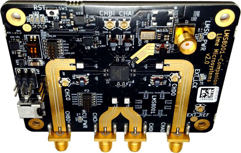
An EMI shield PCB is a printed circuit board designed with structural or physical shielding measures to suppress electromagnetic interference. The shielding may be achieved through multilayer stack-up optimization, grounded shielding cans, via fencing, conductive coatings, or a combination of these techniques.
Modern electronics operate at increasingly higher frequencies. Fast edge rates, switching regulators, dense layouts, and wireless modules generate unintended electromagnetic radiation.
Without proper control, this radiation can:
- Distort high-speed signals
- Trigger instability in analog circuits
- Interfere with wireless modules
- Cause failure in CE, FCC, or automotive EMC testing
The role of PCB EMI shielding is not simply to “block noise.” It is to control electromagnetic energy flow inside the board, manage return paths, and isolate sensitive circuits from aggressive ones.
In high-performance designs, shielding is part of the architecture—not an afterthought.
What Causes EMI in PCB Designs?
EMI rarely comes from a single mistake. It usually results from cumulative layout and structural decisions.
Common root causes include:
1. Discontinuous Return Paths
When a high-speed signal crosses a split plane or changes reference layers without proper stitching vias, return current is forced to find an alternate path. This creates loop area, which directly increases radiation.
2. Poor Stack-Up Planning
If signal layers are not tightly coupled to a solid ground plane, electromagnetic fields extend further into space, increasing emissions.
3. Switching Power Supplies
High di/dt and dv/dt transitions in DC-DC converters generate wideband noise. Without careful layout and shielding, these become major EMI sources.
4. Inadequate Ground Stitching
Insufficient ground vias around board edges or RF sections reduce containment effectiveness.
In most real-world projects, EMI problems are layout-driven rather than component-driven.
What Is PCB EMI Shield and How Does It Work?
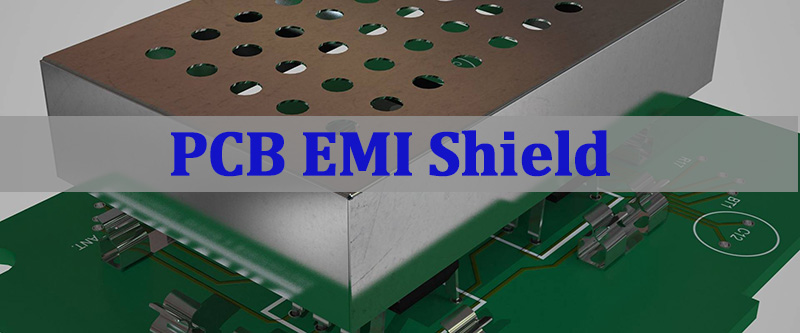
The term PCB EMI shield generally refers to physical shielding structures added to a circuit board—most commonly metal shielding cans soldered over sensitive or noisy circuit sections.
The underlying physics is based on the Faraday cage principle: a conductive enclosure redistributes electromagnetic fields, preventing radiation from escaping or external interference from penetrating.
The shield works by:
- Reflecting incident electromagnetic waves
- Absorbing part of the energy
- Providing a low-impedance grounding path
- Reducing electric field coupling
However, a shielding can is only effective if it is properly grounded. Poor soldering, incomplete ground continuity, or high contact resistance can significantly reduce shielding performance.
Effective shielding is a system-level solution—not just a metal cover.
What Are the Different Types of PCB EMI Shielding Methods?
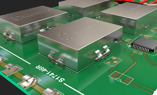
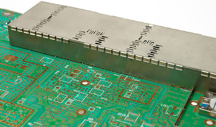
Soldered Shielding Cans
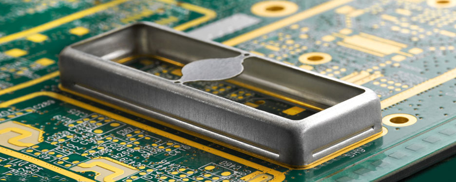
Surface-mounted metal shielding cans are the most common method. These are typically made of tin-plated steel or nickel silver and are reflow-soldered onto grounded pads.
They are widely used in:
- WiFi and Bluetooth modules
- GPS circuits
- Cellular communication boards
- RF front-end designs
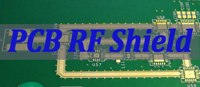
Via Stitching (Ground Fencing)
Ground vias placed closely around RF traces or board edges form a containment wall. This reduces edge radiation and improves high-frequency confinement.
Multilayer Stack-Up Shielding
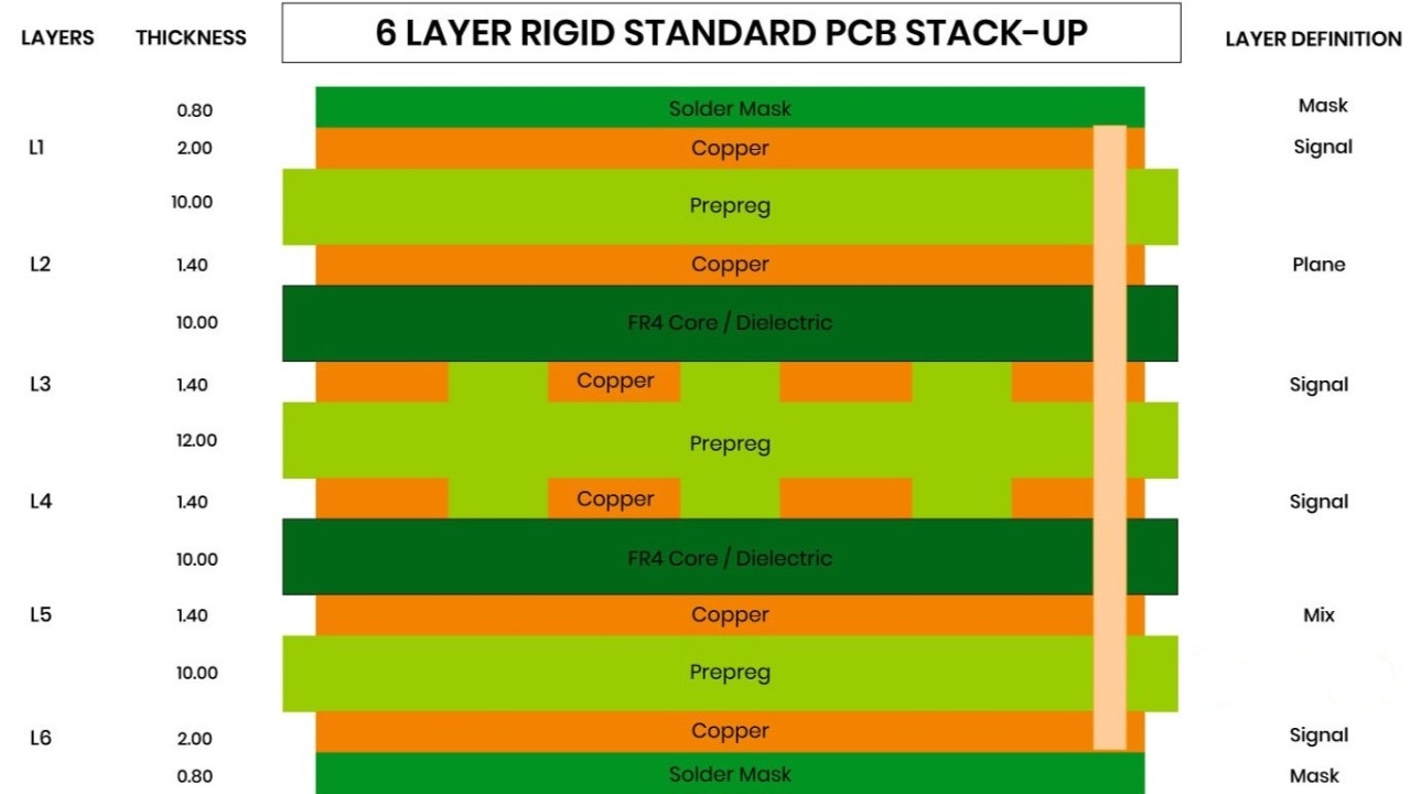
Carefully planned layer stacks—with signal layers adjacent to uninterrupted ground planes—dramatically reduce field propagation.
For example:
- 4-layer: Signal / GND / Power / Signal
- 6-layer: Signal / GND / Signal / Power / GND / Signal
This structural shielding often reduces emissions before a physical shield is even added.
EMI Shield PCB vs Heavy Copper PCB: Which One Is More Effective?
These two approaches solve different problems.
| Aspect | EMI Shield PCB | Heavy Copper PCB |
|---|---|---|
| Primary goal | Suppress radiation | Increase current capacity |
| High-frequency control | Strong | Limited |
| Thermal handling | Moderate | Excellent |
| Power noise suppression | Structural | Indirect |
Heavy copper improves thermal and current performance, but it does not inherently solve radiated EMI. In high-power designs, combining both approaches may be necessary.
How Does Stack-Up Design Influence EMI Performance?
Stack-up design is one of the most powerful EMI control tools available.
A well-structured stack-up:
- Minimizes loop area
- Controls impedance
- Provides stable reference planes
- Improves return current containment
Practical recommendations include:
- Avoid splitting ground planes under high-speed traces
- Keep signal layers tightly coupled to reference planes
- Use stitching vias near layer transitions
- Isolate RF sections physically and electrically
In many cases, optimizing stack-up reduces the need for additional shielding hardware.
How Should You Design PCB EMI Shielding for RF and High-Speed Applications?
For RF and high-speed boards, shielding must be integrated into layout strategy.
Key design considerations:
- Maintain controlled impedance routing
- Avoid sharp corners in RF traces
- Surround RF regions with via fences
- Keep high-current switching nodes away from sensitive analog areas
- Provide continuous ground pads for shielding cans
Design review before fabrication is critical. Shield placement should align with component height, reflow profile compatibility, and mechanical constraints.
What Materials Are Used in EMI Shield PCB Manufacturing?
Material selection influences both shielding effectiveness and manufacturability.
Common materials include:
- Tin-plated steel (cost-effective, widely used)
- Nickel silver alloys (better corrosion resistance)
- High-Tg FR-4 substrates
- ENIG or ENEPIG surface finishes for stable grounding
Shield solderability, oxidation resistance, and mechanical rigidity must be evaluated. Inconsistent plating thickness or poor pad finish can reduce grounding performance.
How Does a Professional PCB Manufacturer Validate EMI Shield PCB Quality?
Manufacturing quality directly impacts shielding performance.
Professional validation typically includes:
- AOI inspection for solder continuity
- X-ray analysis for hidden joint verification
- Ground continuity testing
- Pull-strength testing for shield adhesion
- Process-controlled reflow profiling
In advanced production environments, shielding integrity is verified before full-scale manufacturing.
When Should EMI Shielding Be Added to a PCB?
Shielding is recommended when:
- Operating frequencies exceed 100 MHz
- The design includes RF transceivers
- High-speed digital interfaces are present
- The product must pass CE, FCC, or automotive EMC standards
- Switching regulators operate near sensitive analog circuits
Early integration of shielding during design reduces redesign risk later.
What Are the Common Manufacturing Challenges of EMI Shield PCB?
Manufacturing EMI shield PCB assemblies involves several technical challenges:
- Incomplete solder wetting on shield frames
- Warping during reflow
- Oxidation affecting ground contact
- Shield deformation during handling
- Inconsistent ground pad design
These issues require precise SMT process control, stable reflow temperature curves, and experienced engineering oversight.
How to Choose a Reliable EMI Shield PCB Manufacturer?
When selecting a manufacturer, consider:
- In-house PCB and PCBA capability
- Experience with RF and high-frequency boards
- Shielding can sourcing and customization options
- DFM support for grounding optimization
- Stack-up engineering consultation
A manufacturer that understands both electromagnetic theory and practical assembly constraints can significantly reduce risk during certification.
To conclude, an EMI shield PCB is more than a metal cover on a board. It is a coordinated approach involving stack-up planning, grounding architecture, material selection, and precision manufacturing.
When designed and manufactured correctly, PCB EMI shielding improves signal stability, enhances product reliability, and supports successful EMC certification. For high-frequency, RF, industrial, automotive, or medical electronics, early collaboration with an experienced manufacturer can prevent costly redesign cycles and accelerate time to market.
If your project involves EMI-sensitive circuits or requires compliance testing, it is worth evaluating shielding strategy at the design stage rather than treating it as a corrective measure later. For inquiries related to EMI Shielding PCB design, prototyping, or assembly, please do not hesitate to contact us via sales@bestpcbs.com. Our team is here to provide expert support.
FAQs About EMI Shield PCB
Does EMI shielding significantly increase cost?
Typically, shielding adds 5–15% depending on shield size, material, and assembly complexity.
Can shielding cans be removed for debugging?
Some designs use removable frame-and-cover structures for test access.
Is PCB EMI shielding enough without enclosure shielding?
PCB shielding controls localized interference. For full compliance, enclosure design must also be considered.
Do all products require EMI shielding?
Low-frequency or simple analog designs often do not. High-speed or wireless systems typically do.