

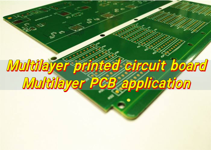
Multilayer printed circuit board is a circuit board built from three or more conductive copper layers laminated together with insulating material. Unlike single- or double-sided boards, multilayer PCBs stack internal signal and power layers between outer layers, allowing complex circuits to fit into a much smaller footprint.
What is a multilayer PCB?
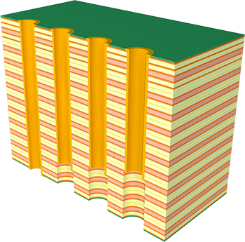
Multilayer printed circuit board is a circuit structure that combines three or more conductive copper layers into a single, unified board. These layers are separated by insulating materials and bonded together under heat and pressure to form a compact electrical platform.
In practical electronics, a multilayer printed circuit board allows designers to place signal layers, power planes, and ground planes in carefully controlled positions. This internal structure improves electrical stability while reducing electromagnetic interference.
As products continue to shrink while performance expectations rise, multilayer printed circuit boards have become the backbone of modern electronic systems. Smartphones, medical equipment, automotive electronics, and industrial controls all rely on this technology to meet demanding requirements.
From a manufacturing standpoint, multilayer PCB production requires precise process control. Layer alignment, dielectric thickness, copper balance, and via reliability all influence final performance. At EBest Circuit (Best Technology), multilayer printed circuit boards are produced as part of a fully integrated Turnkey EMS service, ensuring design intent and production reality stay aligned.
How to identify multi-layer PCB?
Identifying a multi-layer PCB usually starts with visual inspection, but surface clues alone are often not enough. Unlike single-layer boards, multilayer designs hide most of their complexity inside the board structure.
One common indicator is the presence of plated through holes that connect multiple layers. These vias typically appear filled or copper-lined, suggesting internal interconnections. Dense via fields are often associated with multilayer printed circuit boards, especially in high-speed or high-density designs.
Board thickness can also provide hints. Multilayer PCBs are often thicker than simple boards, even when designed for compact products. The additional dielectric layers add measurable depth.
For accurate identification, manufacturers use cross-sectional analysis or fabrication drawings. These clearly show the number of copper layers and their arrangement. It is defined, documented, and verified before production begins.
How can you tell how many layers a PCB has?
Determining the exact number of layers in a PCB requires more than observation. The most reliable method is reviewing the fabrication documentation, where the stack-up is clearly specified. This document lists each copper layer, dielectric material, and thickness in sequence.
In a production environment, cross-section testing is commonly used. A small sample of the board is cut and polished so the internal layers can be counted under magnification. This method is precise and often used for quality validation in multilayer PCB manufacturing.
Electrical testing can also provide indirect clues. The number of reference planes affects impedance behavior and signal integrity. Experienced engineers can infer layer complexity based on performance characteristics, but this approach is supplementary rather than definitive.
For customers working with Turnkey EMS providers like EBest Circuit (Best Technology), layer count transparency is standard practice. Every multilayer printed circuit board process begins with a confirmed stack-up, ensuring consistency from prototype to volume production.
What material is used for multilayer PCB?
The most common material used in multilayer printed circuit boards is FR-4, a glass-reinforced epoxy laminate. FR-4 offers a balance of mechanical strength, electrical stability, and cost efficiency.
For more demanding environments, alternative materials are often selected. High-Tg laminates improve thermal performance and dimensional stability. Low-loss materials support high-speed signal transmission by reducing dielectric losses.
Copper foil is used for conductive layers, with thickness selected based on current requirements and impedance design. The dielectric layers between copper planes control capacitance, signal propagation, and thermal behavior. Material selection directly influences power bus decoupling on multilayer printed circuit boards, especially in high-current designs.
How to design a multilayer PCB?
Designing a multilayer PCB begins with system requirements, not routing convenience. Engineers first define signal integrity goals, power distribution needs, and thermal constraints.
A well-designed multilayer printed circuit board separates functions across layers. Signal layers are placed adjacent to solid reference planes. Power planes are distributed to minimize voltage drop and noise.
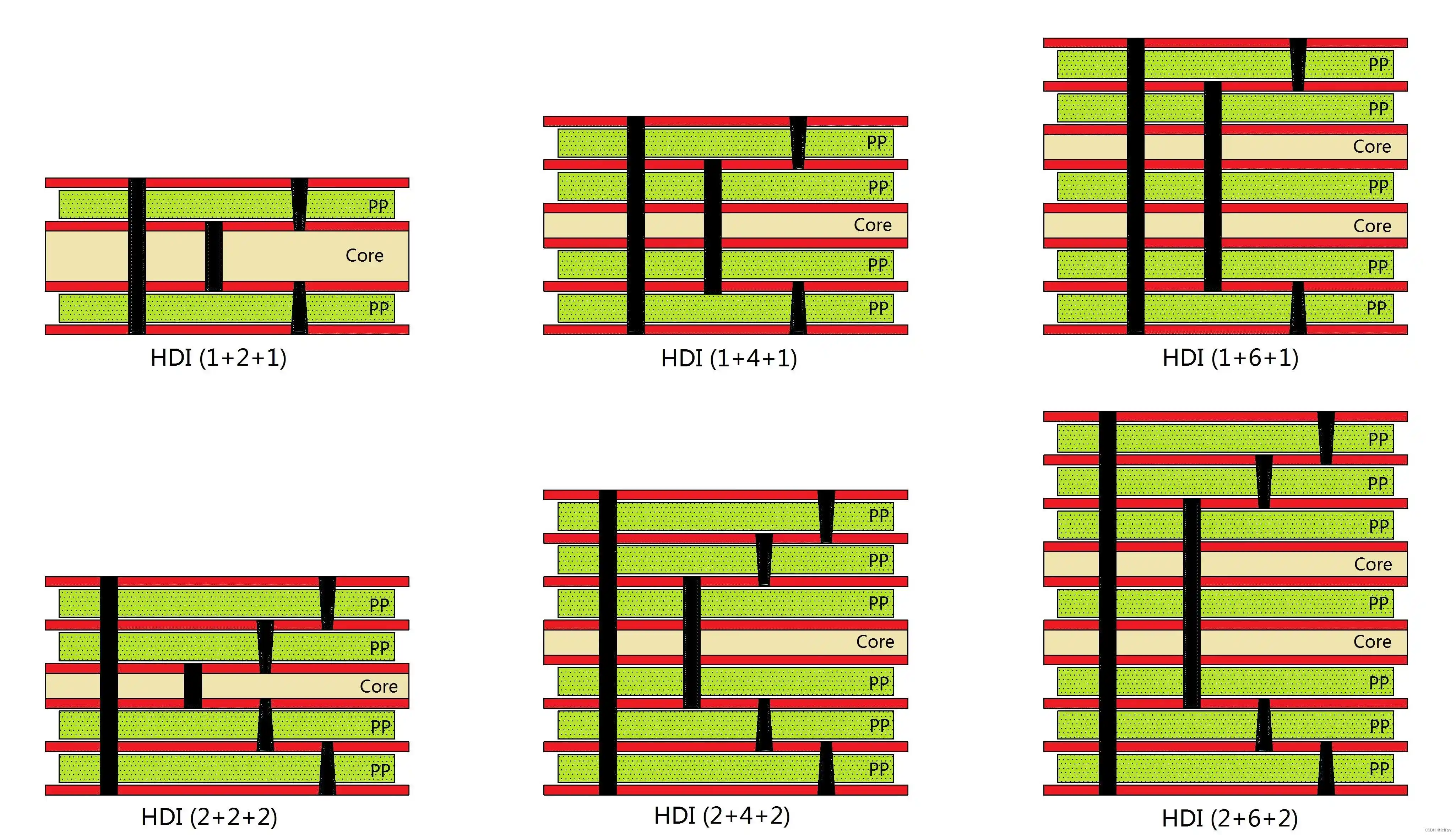
Via strategy is another critical element. Through vias, blind vias, and buried vias each serve different purposes. High-speed signal optimization at differential vias in multilayer printed circuit boards requires careful geometry control to maintain impedance and timing balance.
Simulation plays an important role in modern design. Analytical evaluation of via plate capacitance for multilayer printed circuit boards and packages helps engineers predict parasitic effects before fabrication.
At EBest Circuit (Best Technology), design support is closely tied to manufacturing expertise. Design-for-manufacturability reviews ensure that multilayer PCB designs translate smoothly into reliable production, even for complex stack-ups.
What is the highest number of layers in a PCB?
There is no absolute limit to the number of layers in a PCB, but practical constraints define realistic boundaries. Commercial multilayer printed circuit boards commonly range from four to twenty layers. Advanced systems may use thirty or more layers when required.
In high-performance computing and aerospace applications, extremely high layer counts have been achieved. These designs demand precise control of materials, lamination cycles, and registration accuracy. Each added layer increases complexity and cost.
More layers provide routing flexibility and power integrity, but they also introduce manufacturing challenges. Balance is essential.
Experienced manufacturers guide customers toward optimal solutions rather than maximum complexity. The goal is not to use the most layers, but the right number of layers to meet performance and reliability goals.
What is the purpose of having multiple layers in a PCB?
The primary purpose of multiple layers in a PCB is functional separation. Different electrical roles are assigned to dedicated layers, improving performance and predictability. Signal layers carry data. Power layers distribute energy. Ground layers provide stable references.
This separation enhances signal integrity by reducing noise coupling and crosstalk. It also supports efficient power distribution, which is critical in modern electronics with fast switching devices.
Multilayer printed circuit boards also enable compact product design. By routing signals vertically through vias, designers reduce board area while maintaining functionality.
Thermal performance is another key benefit. Internal copper planes act as heat spreaders, helping manage temperature rise. When designed correctly, multilayer structures contribute directly to long-term reliability.
What are the advantages of multilayer PCBs?
Multilayer PCBs offer several compelling advantages that make them the preferred choice for advanced electronics.
- One major benefit is improved electrical performance. Shorter signal paths and controlled impedance support high-speed operation.
- Another advantage is mechanical stability. Laminated layers create a rigid structure that resists warping and vibration.
- Design flexibility also increases with layer count. Engineers can route complex circuits without overcrowding, improving yield and manufacturability.
- From a system perspective, multilayer printed circuit boards enable integration. More functionality fits into less space, reducing assembly complexity.
How do multilayer PCBs work?
Multilayer PCBs work by distributing electrical functions across stacked conductive layers. Signals travel through copper traces on designated layers, while power and ground planes provide stable electrical environments.
Vias connect these layers vertically, creating three-dimensional routing paths. This structure allows complex interconnections without excessive surface congestion.
The internal planes also act as capacitive elements. Power bus decoupling on multilayer printed circuit boards benefits from closely spaced power and ground layers.
Manufacturing precision ensures that each layer aligns correctly. Lamination bonds layers into a single unit, while drilling and plating create reliable interconnections. The result is a cohesive electrical platform designed to perform consistently.
What is the difference between single layer and multilayer PCB?
The difference between single layer and multilayer PCB lies in complexity, capability, and application scope. A single-layer board has one conductive layer and is suitable for simple circuits. It offers low cost and straightforward manufacturing.
A multilayer PCB, by contrast, supports complex routing and higher performance. Multiple layers enable better signal control, power distribution, and noise reduction.
Single-layer boards struggle with high-speed signals and dense layouts. Multilayer printed circuit boards handle these challenges with structured stack-ups and dedicated planes.
The choice depends on requirements. Simple products benefit from simplicity. Advanced systems demand multilayer solutions.
Common multilayer PCB application scenarios
Multilayer PCB application spans nearly every advanced electronic sector.
- Consumer electronics rely on multilayer printed circuit boards to support compact, feature-rich devices. Smartphones and tablets are prime examples.
- In medical electronics, multilayer designs support precision, reliability, and miniaturization. Diagnostic equipment and monitoring systems depend on stable signal integrity and controlled power distribution.
- Automotive systems use multilayer PCBs for safety-critical functions. Engine control units, driver assistance systems, and infotainment platforms all benefit from multilayer architecture.
- Industrial equipment also relies heavily on multilayer PCB application. Automation, robotics, and power control systems require robust designs that withstand harsh environments.
Across all these scenarios, manufacturing consistency matters. EBest Circuit (Best Technology) integrates multilayer PCB manufacturing with assembly and testing, delivering complete Turnkey EMS solutions that support diverse applications.
Conclusion:
Multilayer printed circuit boards form the foundation of modern electronics. They enable compact design, stable performance, and functional integration across industries. From material selection to stack-up design, every decision shapes reliability and efficiency.
Choosing the right partner is just as important as choosing the right layer count. If you are planning a multilayer PCB project or need full Turnkey EMS support, EBest Circuit (Best Technology) is ready to help.
For technical consultation or quotations, contact sales@bestpcbs.com