pcb
Home > Blog

Posts Tagged ‘Heavy copper PCB manufacturers’

Heavy Copper PCB Manufacturers, Extreme Copper PCB
Sunday, March 30th, 2025

Heavy copper PCB manufacturers play a crucial role in creating circuit boards that handle high currents, distribute heat efficiently, and meet the needs of demanding industries. Whether you’re looking for extreme copper PCBs, 20oz copper PCBs, or a custom copper core PCB, understanding the factors that affect their design, quality, and assembly process will help you choose the proper manufacturer for your needs.

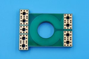
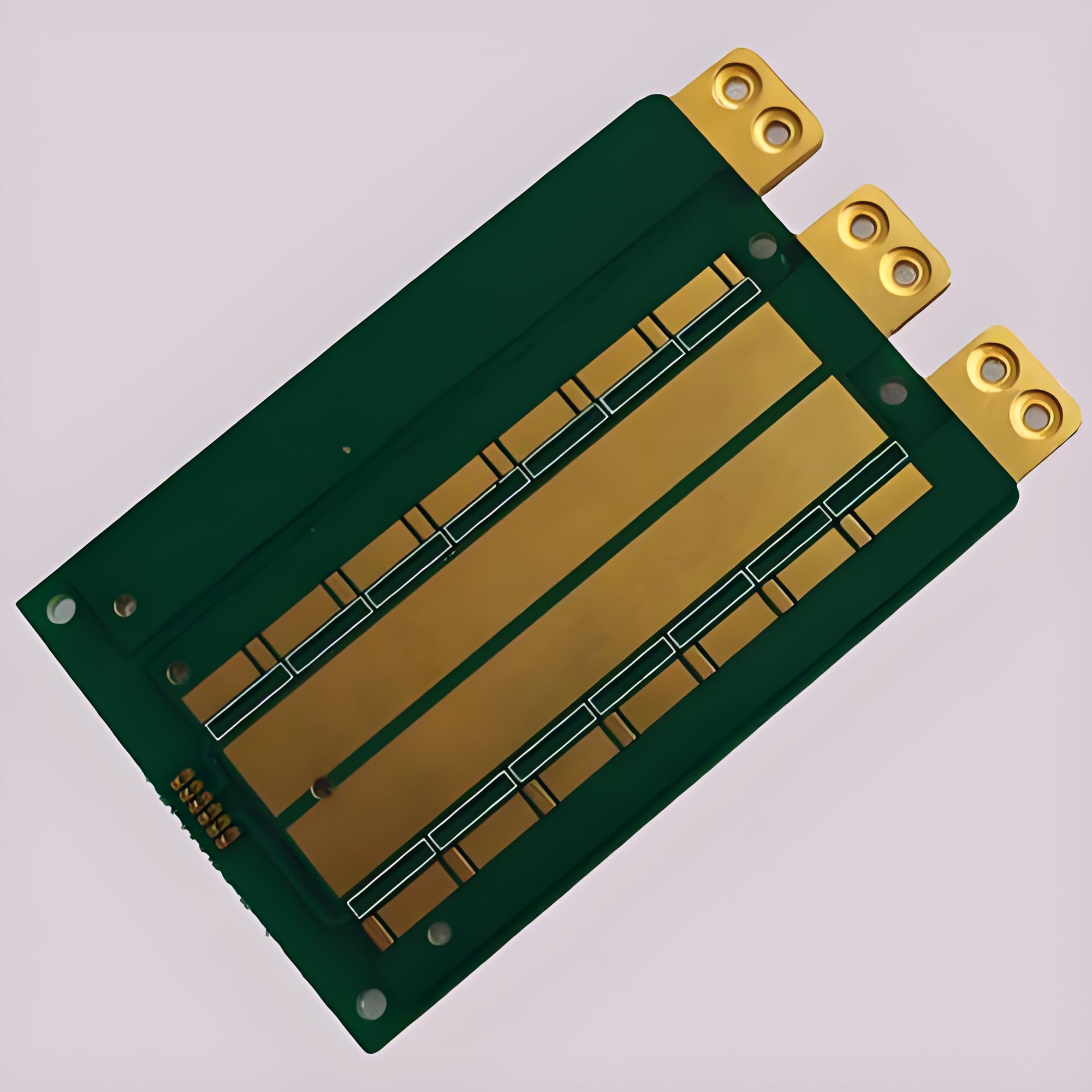
Heavy copper PCB (Printed Circuit Board) is a go-to solution for high-performance applications that require durability. Best Technology provides high-quality Heavy copper PCB in the PCB industry. We provide rapid prototypes within 24-48 hours. We have offered more than 1,200 customers in more than 60 countries & areas the fast turnaround heavy copper PCB service. We provide both normal delivery service and fast service, and urgent boards can be shipped out within 24 hours! Best Technology is one of the professional heavy copper PCB Manufacturers, if you need heavy copper PCB design, prototype, or assembly, pls feel free to reach out to Best Technology at sales@bestpcbs.com at any time.

Heavy Copper PCB Manufacturers, Extreme Copper PCB

What Design Factors Do Heavy Copper PCB Manufacturers Consider for Reliability?

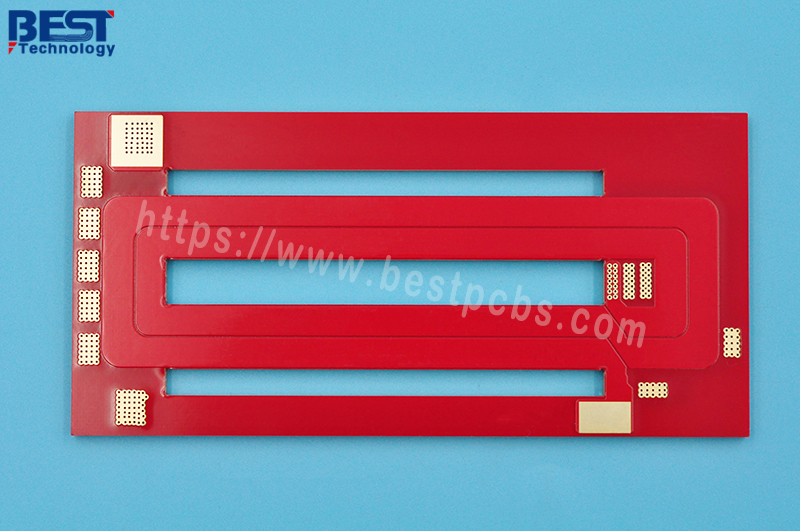
When designing heavy copper PCBs, manufacturers have to consider a wide range of factors to ensure the board performs reliably over time. Copper thickness, trace width, and the material’s ability to handle high current loads are just a few of the key considerations.

The first important design factor is the copper trace width. For high-current applications, manufacturers use wider copper traces to handle the increased load without overheating. This is especially important in industries like automotive, telecommunications, and power electronics, where PCB durability and performance are critical.

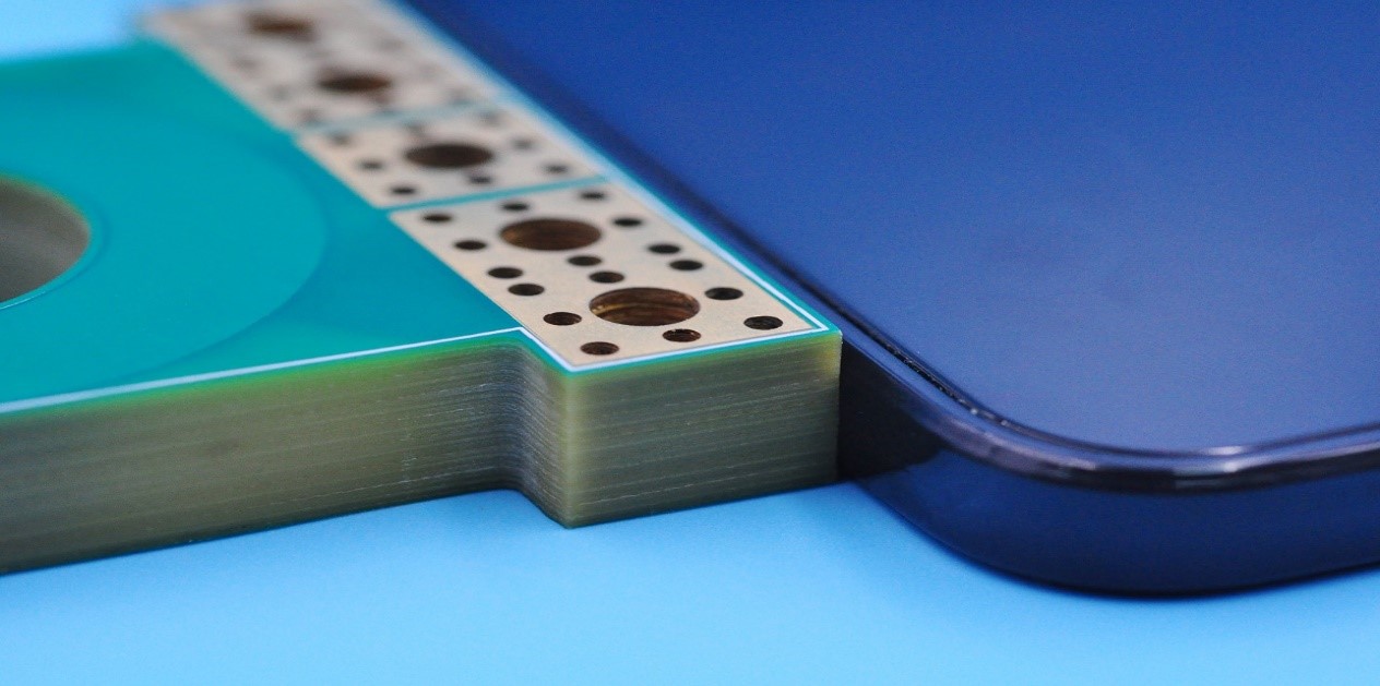
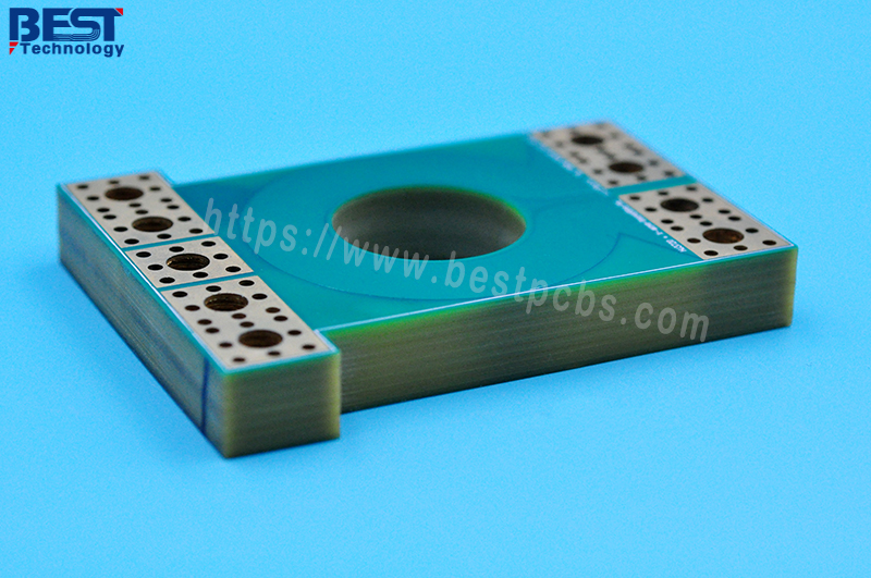
Another crucial aspect is layer stacking. Manufacturers use multiple layers in heavy copper PCBs to ensure that the heat generated by high currents can dissipate efficiently. This helps prevent thermal buildup, which can lead to failure or damage to the PCB. The layers are carefully arranged to maximize heat dissipation and ensure optimal performance under load.

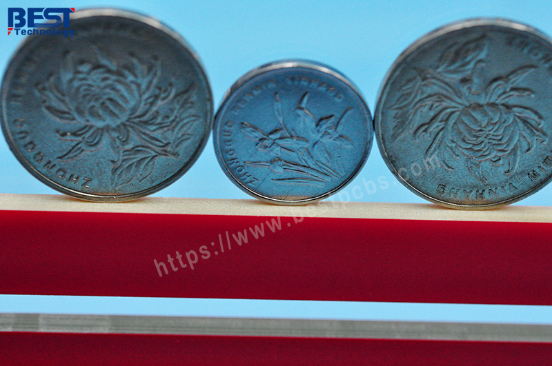
Heat dissipation techniques are also a major design factor. A properly designed heavy copper PCB uses advanced techniques, such as copper coin technology, which places thick copper elements within the PCB to efficiently absorb and dissipate heat.

Heavy Copper PCB Manufacturers

Where to Find Reliable Heavy Copper PCB Manufacturers for PCBs?

Finding the right manufacturer is key to ensuring you get a high-quality heavy copper PCB that meets your specifications. The process of identifying reliable manufacturers often starts with online research. There are numerous online directories, trade shows, and industry events where you can find reputable heavy copper PCB manufacturers.

Customer reviews and feedback play a significant role in identifying reliable manufacturers. Look for companies that have a proven track record in producing high-quality heavy copper PCBs. Best Technology, for instance, has built a strong reputation over 18 years, delivering excellent products to industries around the world.

Industry certifications also signal reliability. Established manufacturers often have certifications such as ISO 9001, UL, and IPC, which indicate their adherence to international quality standards.

Networking is another great way to find trusted manufacturers. Industry forums, LinkedIn, and professional groups offer recommendations from other businesses that have worked with these manufacturers.

Extreme Copper PCB

What Certifications Should Reliable Heavy Copper PCB Manufacturers Have?

Choosing a reliable heavy copper PCB manufacturer requires understanding the certifications they hold. Certifications are an assurance that the manufacturer follows quality control procedures and complies with industry standards.

The ISO 9001 certification is a widely recognized standard that shows a manufacturer’s commitment to quality management. It ensures that the manufacturer has consistent processes in place to deliver high-quality products.

The UL certification is another important factor, especially for PCBs that will be used in safety-critical applications. UL certification indicates that the manufacturer meets safety standards and that their products are safe for use in electrical applications.

Lastly, IPC certifications (such as IPC-A-600 and IPC-2221) demonstrate that the manufacturer follows best practices for PCB design, assembly, and inspection. These certifications ensure that the manufacturer produces PCBs that meet industry standards for performance and reliability.
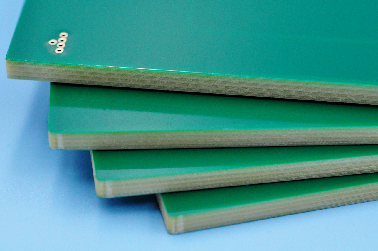
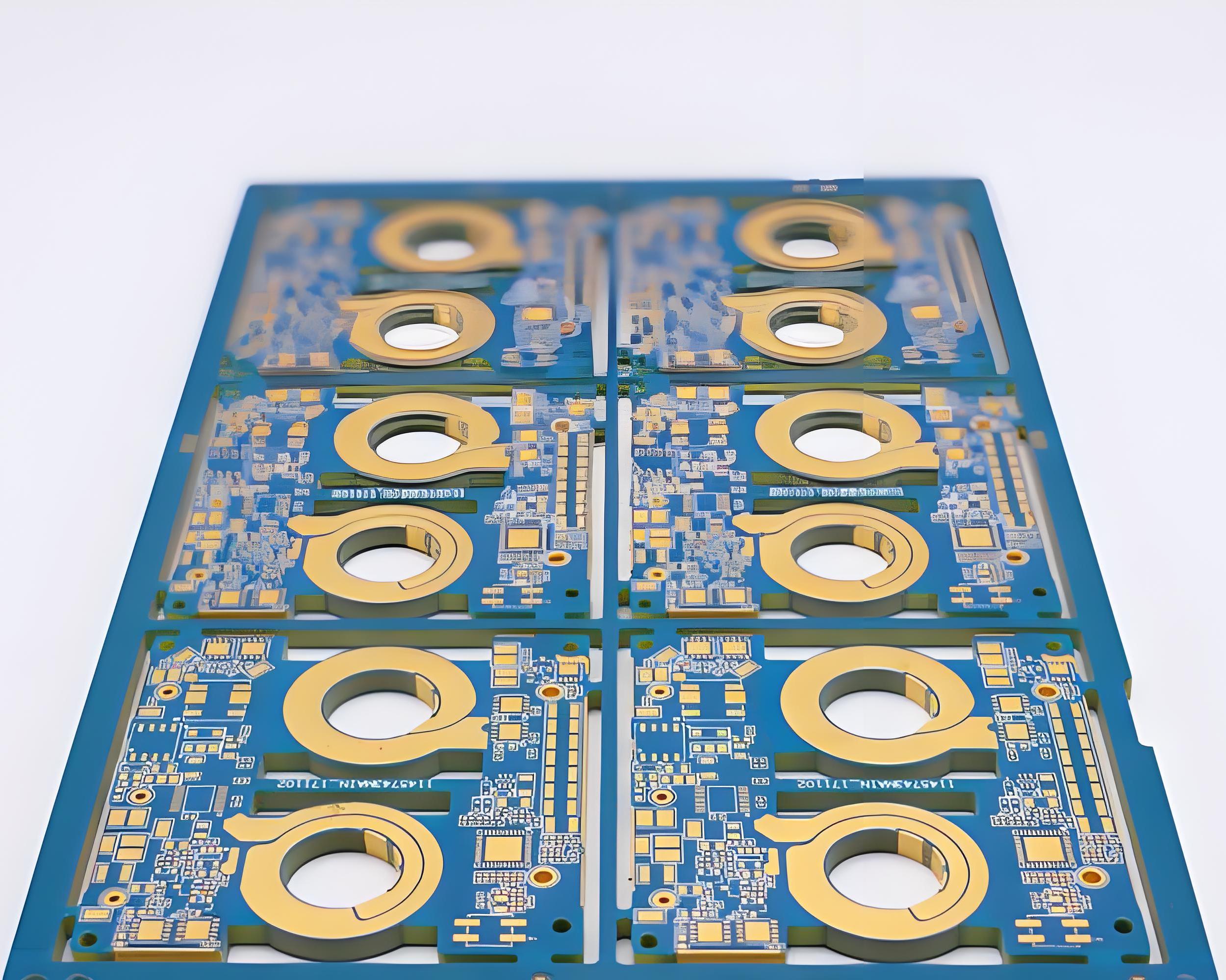
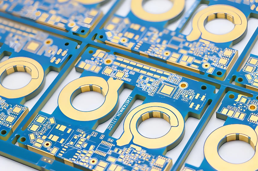
What Is the Thickness of Copper in Best Technology?

Best Technology offers a range of copper thickness options tailored to different applications. Below is the capability of heavy copper PCB for your reference:

  • Base material: FR4/Aluminum
  • Copper thickness: 4 OZ~10 OZ
  • Extreme Heavy Copper: 20~200 OZ
  • Outline: Routing, punching, V-Cut
  • Solder mask: White/Black/Blue/Green/Red Oil
  • Surface finishing: Immersion Gold, HASL, OSP
  • Max panel size: 580*480mm(22.8″*18.9″)

Best Technology doesn’t do “one-size-fits-all.†Our copper range fits every need. 2 oz (70 µm) is commonly used in consumer gadgets like phones, and routers. 4–10 oz heavy copper PCB is suitable for industrial applications like solar inverters.  20–200 oz extreme copper PCB is perfect for power substations and other areas that require heat dissipation and high current-carrying capacity. By customizing the copper thickness, Best Technology ensures that each PCB meets the specific needs of its customers, whether for high-frequency applications or power electronics.

How Thick Is 2 oz of Copper for PCB?

A 2 oz copper PCB typically has a thickness of around 70 microns (2.8 mils). While this is considered a mid-range thickness, it offers significant advantages over standard copper PCBs. The thicker copper enables the PCB to handle more current and provides better thermal performance, making it ideal for applications in industrial machinery, power supplies, and automotive systems.

The added copper thickness also improves the board’s resistance to thermal stress, which is particularly important in environments where heat is generated due to high power loads.

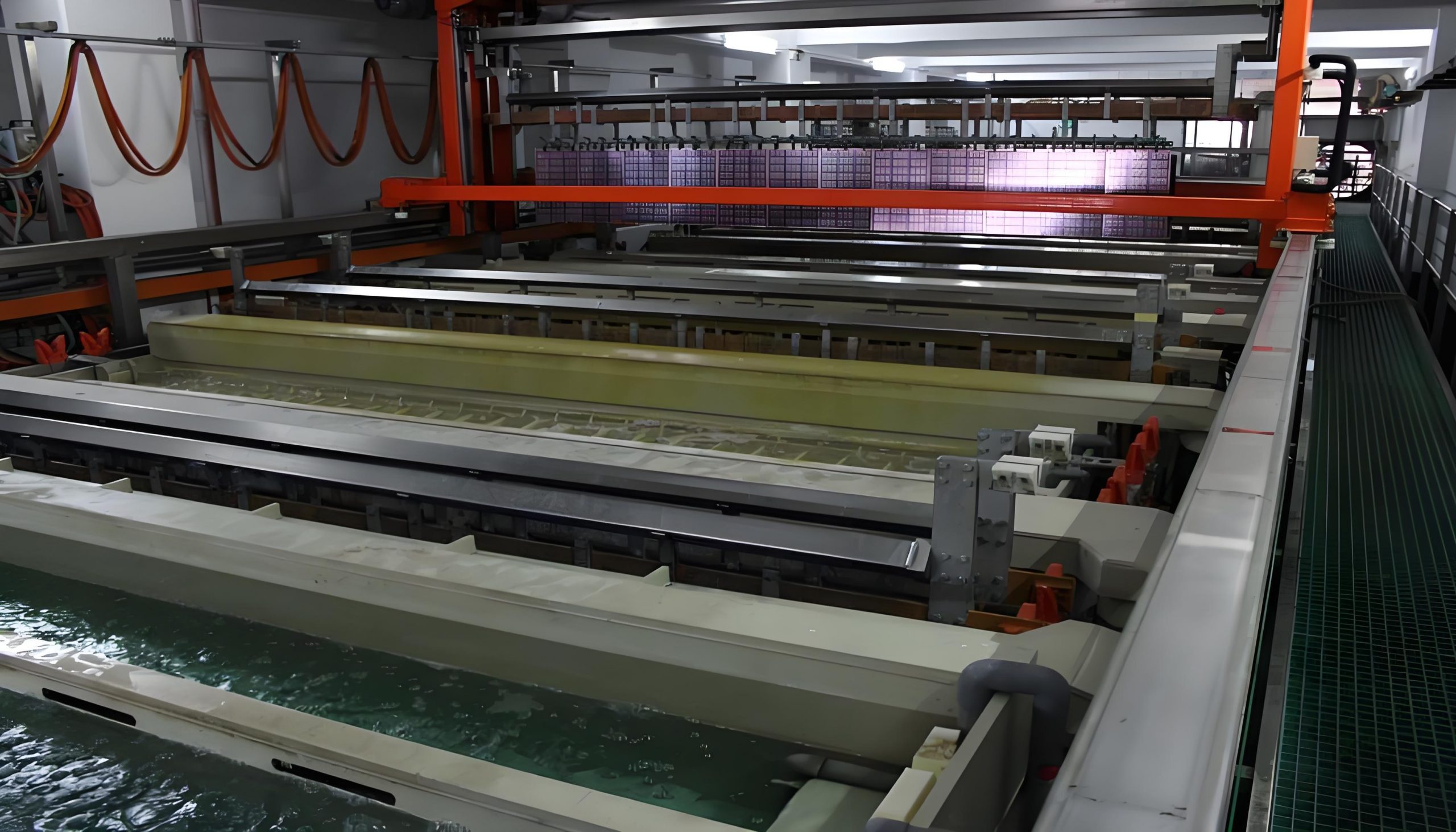
How Do Heavy Copper PCB Manufacturers Ensure Quality and Durability?

Ensuring the quality and durability of heavy copper PCBs is a multi-step process. From the initial design phase to the final assembly, manufacturers must employ strict quality control measures.

At Best Technology, advanced technologies like automated optical inspection (AOI) and X-ray inspection are used to detect potential defects early in the production process. These tools ensure that any issues are identified and corrected before they affect the final product.

Manufacturers also use high-quality materials like copper foil and ensure that the lamination process is carried out under precise conditions to avoid defects. Each PCB undergoes thorough testing to verify its electrical properties, mechanical strength, and heat dissipation capabilities.

Heavy Copper PCB Manufacturers

How to Choose a Heavy Copper PCB Manufacturer?

Choosing the right heavy copper PCB manufacturer requires careful consideration of several factors:

  • 1. Experience: Look for manufacturers with experience in producing heavy copper PCBs, especially for the type of application you’re targeting.
  • 2. Technology: Ensure the manufacturer has the latest technology for PCB design, fabrication, and testing.
  • 3. Customer Service: A good manufacturer will offer support throughout the entire process, from design to assembly.
  • 4. Prototyping: Request prototypes to verify the manufacturer’s capabilities before committing to large-scale production.

By evaluating these factors, you can choose a manufacturer that meets your quality standards and provides a seamless experience from start to finish.

Finally, heavy copper PCB manufacturers are essential partners for businesses in need of high-performance and durable PCBs. Best Technology stands out as a reliable provider of heavy copper PCBs, offering customized solutions and unparalleled expertise. Whether you need extreme copper PCBs or 20oz copper PCBs, choosing the proper manufacturer ensures the success and longevity of your products.

Do you need a heavy copper PCB solution? Just feel free to contact Best Technology at sales@bestpcbs.com at any time for expert guidance, exceptional quality, and fast delivery.

You may also like

What is heavy copper pcbs?
Friday, December 13th, 2024

What is heavy copper pcbs? That is, the copper foil thickness is greater than the conventional standard PCB. Generally speaking, when the copper foil thickness reaches 3 ounces per square foot (oz/ft²) and above, it can be called a heavy copper PCB.

The manufacturing process of heavy copper PCBs is more complicated than that of ordinary PCBs, requiring higher technical levels and professional equipment. Compared with ordinary PCBs, its characteristics are high current carrying, good heat dissipation, high mechanical strength and strong reliability. It is suitable for high-power electronic equipment, harsh working environments and fields with high reliability requirements.

What is heavy copper pcbs?

What is high copper thickness PCB?

High copper thickness PCB refers to a printed circuit board that uses thicker copper foil as the conductive material. In the standard PCB manufacturing process, the thickness of the copper foil is usually determined according to the application requirements, but when the thickness of the copper foil is greater than or equal to 3 ounces, this PCB is called a high copper thickness PCB.

Usually compatible with FR-4 dielectric, mainly used for inner layers rather than outer layers, plated through holes (PTH) usually need to be plugged/filled, and careful registration and lamination are required

Common heavy copper PCB thickness:

  • 2 oz (70 microns)
  • 3 oz (105 microns)
  • 4 oz (140 microns)
  • 6 oz (210 microns)
  • 8 oz (280 microns)
  • 10 oz (350 microns)

Application areas of heavy copper PCB:

  • Automotive electronics: widely used in key electronic devices such as automotive control modules, engine control systems, airbags, etc., because they can withstand high temperature, low temperature, corrosion and other environmental factors.
  • Power circuit: widely used in power modules, DC-DC converters and high power distribution boards, etc., capable of handling high current and high power requirements.
  • Industrial control system: used in high power motor drives, automation equipment and large mechanical control to meet the needs of high conductivity and mechanical strength.
  • Renewable energy systems: used in solar and wind energy systems to ensure stable system operation and reduce failure rates.

What are the advantages of heavy copper PCBs?

  • High conductivity: High copper PCB uses heavy copper foil as the conductive layer. Compared with ordinary PCB, its conductivity is significantly improved, which can carry larger current, reduce resistance loss and improve circuit efficiency.
  • High mechanical strength: Due to the increase in the thickness of copper foil, the mechanical strength of high copper PCB is also improved accordingly, which can withstand greater mechanical stress and impact, and is not easy to deform or damage.
What is heavy copper pcbs?
  • Good heat dissipation performance: High copper PCB can quickly transfer heat from the circuit to the surrounding environment, effectively prevent components from overheating and damage, and improve the reliability and service life of the equipment.

What type of copper is PCB?

There are mainly the following types of copper on PCB: red copper, copper clad plate and inner layer copper.

  • Red copper: Red copper is the earliest material used in circuit boards, and is widely used due to its good processing performance and conductivity. The main component of red copper is copper, and the other components are less, but the disadvantage is that it is easily oxidized and corroded.
  • Copper clad laminate: Copper clad laminate is a layer of copper foil on an inorganic substrate, usually used for double-sided and multi-layer circuit boards. The copper foil ensures the conductivity and connectivity of the circuit board, while the inorganic substrate provides mechanical strength and heat resistance.
  • Inner copper: Inner copper is used in multi-layer circuit boards, which are made of multiple layers of inorganic substrate and copper foil. It is usually used in high-density or high-speed design circuit boards, with better signal transmission performance and higher mechanical strength, but the manufacturing cost is higher.

In addition, there are different types of copper foil in PCB, including electrodeposited copper and rolled copper. Electrodeposited copper has a vertical grain structure and a rougher surface, which is suitable for rigid PCB boards; while rolled copper has a horizontal grain structure and a smoother surface, which is suitable for flexible and high-speed circuit boards.

How thick is 2 oz copper on PCB?

The thickness of 2 oz copper is about 70 microns. In PCB design, copper thickness is usually expressed in ounces (oz), and the thickness of 1 ounce of copper is about 35 microns, so the thickness of 2 ounces of copper is about 70 microns.

The copper thickness standard of PCB board is usually expressed in oz/ft² (ounces/square foot) or um (micrometer). The copper thickness of PCB board has an important impact on the performance and stability of the circuit board. The outer copper thickness mainly affects the stability of signal transmission and the ability to resist electromagnetic interference, while the inner copper thickness affects the signal transmission rate and signal-to-noise ratio.

Generally speaking, the thicker the outer copper thickness, the stronger the stability and signal strength of the circuit board, which is suitable for high-frequency and high-speed occasions; while the thinner the inner copper thickness, the more suitable for high-speed transmission signals, and the thicker the inner copper thickness, the more suitable for low-speed transmission signals and high signal-to-noise ratio signals.

Why use heavy copper PCB?

The main reasons for using heavy copper PCB include the following aspects:

  • Enhanced current carrying capacity: Heavy copper PCB uses a thicker copper layer, which can carry a larger current and reduce resistance and voltage drop. This is especially important for high-power applications or circuits that require high current transmission.
  • Optimize heat dissipation performance: Copper has good thermal conductivity, and a thicker copper layer can more effectively conduct heat away from hot spots and improve heat dissipation efficiency.
  • Improve signal transmission efficiency: Thicker copper layers can reduce losses and reflections during signal transmission and improve signal integrity.
  • Enhance mechanical strength: Thicker copper layers can increase the overall structural strength of PCBs, making them more resistant to physical shock and deformation.
  • Adapt to complex process requirements: Heavy copper PCBs can meet complex circuit design requirements through special process treatments, such as etching, drilling, gold plating, etc., to ensure the accuracy and reliability of circuit boards during manufacturing.

What is the most common copper thickness for PCB?

The most common PCB copper foil thickness is 35 microns. This thickness of copper foil is suitable for most consumer electronics products, can meet daily current and heat requirements, and has a relatively low cost and is suitable for large-scale production.

How are heavy copper PCBs made?

In the initial stage of making heavy copper PCBs, relatively heavy copper foil materials are selected. These copper foils are usually produced by electrolytic copper. During the electrolysis process, copper foils of different thicknesses can be produced by controlling the conditions of electrolysis, such as current density, electrolyte composition, and electrolysis time.

For situations where thicker copper foil is required, multiple lamination methods are used. Multiple layers of copper foil and insulating substrate materials are laminated according to design requirements, and then the copper foil and substrate are tightly combined through a high-temperature, high-pressure lamination process.

Next, the circuit pattern is manufactured on the outer layer of the heavy copper PCB, usually using a photolithography process. After that, according to the design requirements, holes are drilled on the heavy copper PCB to provide conditions for installing components and connecting circuits.

What is heavy copper pcbs?

After the drilling is completed, a metal layer is covered on the hole wall using electroplating technology to achieve a connection between the layers, and a layer of copper foil is electroplated on the hole wall to increase the thickness of the conductor and the surface pad. Next, the dry film and excess copper foil are removed, and chemical etchants are generally used to make the circuit pattern clearer.

Subsequently, the heavy copper PCB is subjected to surface treatment, such as gold plating, tin spraying, etc., to improve welding performance and corrosion resistance. Finally, the finished heavy copper PCB is strictly inspected and tested to ensure that its electrical and mechanical properties are consistent with the design requirements.

Professional Heavy copper PCB manufacturers – BEST Technology

The minimum width and thickness of the heavy copper PCB conductor are mainly determined based on the required current carrying capacity and the maximum temperature rise allowed for the conductor. From the perspective of its size specifications and actual manufacturing process, the routing of the circuit board may not be a regular rectangular shape.

What is heavy copper pcbs?

It is worth noting that the thicker copper conductor will significantly increase the overall thickness of the circuit board to a large extent. In terms of manufacturing process, the additive method (electroplating) process has certain advantages over the subtractive method (etching) process, but at the same time, its cost is relatively higher.

BEST Technology process capabilities:

  • Substrate: FR4/Aluminum
  • Copper thickness: 4OZ~10OZ
  • Extremely heavy copper thickness: 20~200 OZ
  • Contour: Milling, Punching, V-Cut
  • Solder mask: White oil/Black oil/Blue oil/Green oil/Red oil
  • Surface treatment: Immersion gold, tin spraying, OSP
  • Maximum panel size: 580*480mm(22.8″*18.9″)

Heavy copper PCB occupies an important position in the electronics field with its unique characteristics. With high current carrying capacity, good heat dissipation performance, higher mechanical strength and excellent reliability, it has become an ideal choice for many high-demand application scenarios. From power electronics to automotive electronics, from aerospace to medical equipment and communications, heavy copper PCB plays a key role.

You may also like