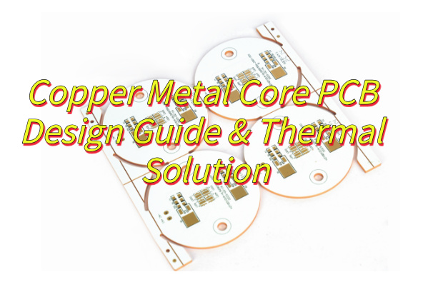
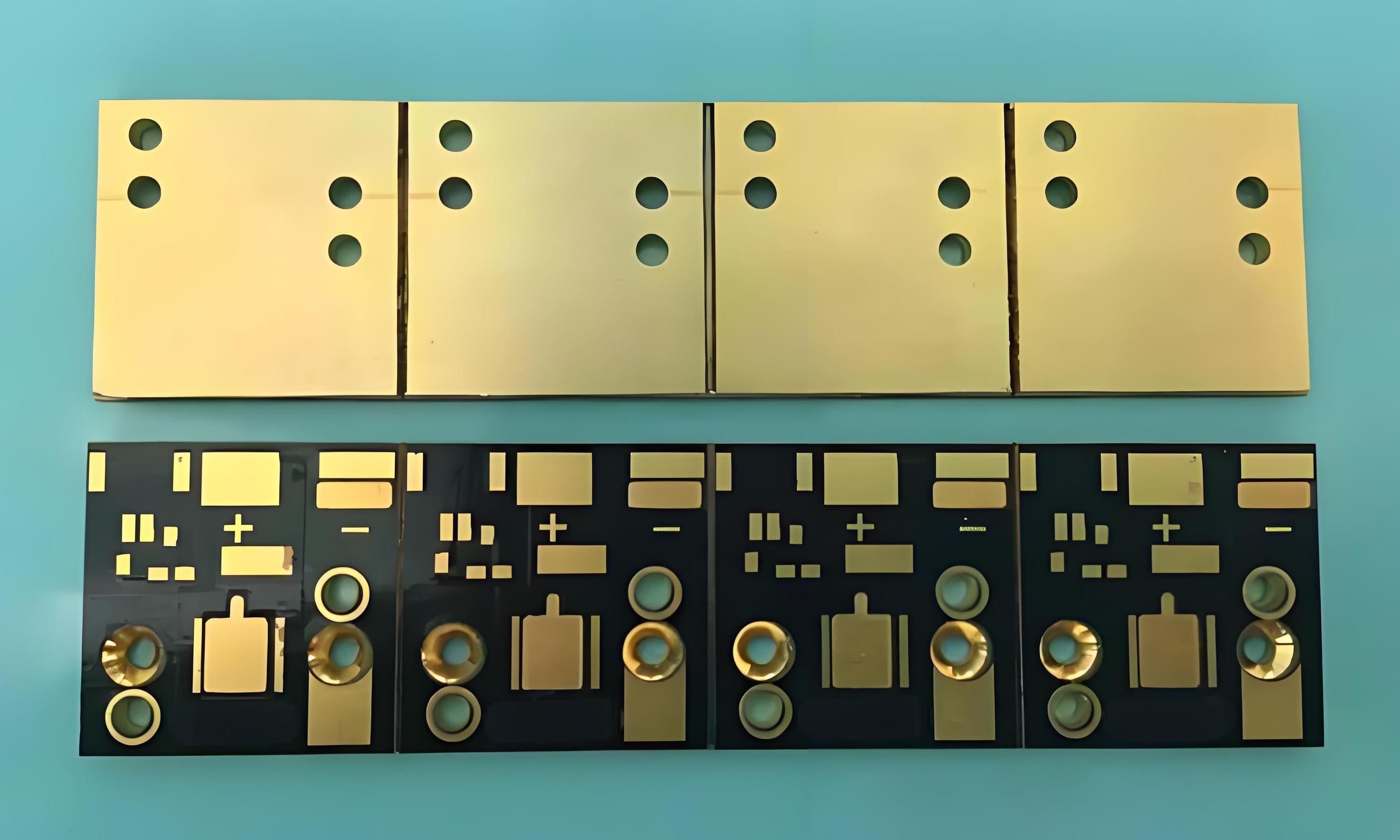
PCB copper core stands out among other PCB types due to its high thermal and power capabilities. These boards are designed to operate in harsh environments, offering exceptional durability and reliability.
Maybe you have these worries and concerns:
- Can the copper thickness and thermal conductivity of copper core PCBs be precisely tailored to meet specific requirements?
- How can I avoid delamination and oxidation of the copper core? How can I resolve issues if they arise?
- Can I guarantee sample or batch delivery?
- Are there any industry examples? Can I receive a 24-hour response to after-sales technical questions?
BEST Technology can solve your problem:
- We support custom copper thicknesses from 0.5-10 ounces, and precisely match power requirements through zoned thermal design.
- We utilize vacuum lamination and an anti-oxidation coating (such as OSP or immersion gold) to ensure interlayer bonding strength ≥1.8N/mm² and pass 1000 cycles of -40°C to 125°C temperature cycling testing without delamination. We offer free rework or replacement for delamination and oxidation issues within the warranty period, with a 48-hour response and solution.
- Single- and double-sided boards: 24-48 hours, multi-layer boards: 3-5 days. Batch delivery: Regular orders: 7-10 days, expedited orders: within 3 days.
- This material has been widely used in new energy vehicle BMS systems (10oz copper thickness), industrial inverters (8oz multilayer boards), and 5G base station power modules (6oz copper core). We provide 24-hour remote support to ensure rapid resolution of technical issues.
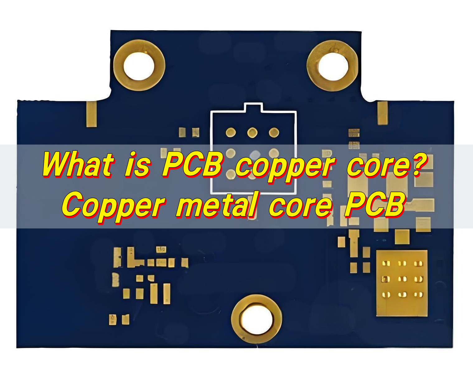
What is a copper core PCB?
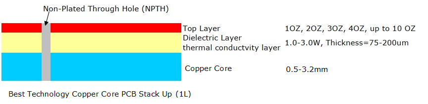
Copper core PCB is a type of printed circuit board with a solid copper layer at its core. Unlike traditional PCBs, where copper is only part of the circuit paths, the core itself is copper. This provides superior thermal conductivity, allowing heat to be efficiently managed in high-power applications.
The copper core acts as a heat spreader. It moves heat away from sensitive components. This prevents overheating and maintains long-term performance. These boards are widely used in LED lighting, automotive electronics, industrial equipment, and power electronics.
Using a copper core also improves the mechanical stability of the board. Components remain securely in place even under heat stress. The copper’s high conductivity ensures that both electrical performance and heat dissipation are optimal.
Why Use a Copper Core PCB?
Modern electronics often produce significant heat, which can reduce efficiency and shorten the life of components. Copper core PCBs solve this problem efficiently.
Here’s why they are used:
- High thermal conductivity: Copper efficiently transfers heat away from components, keeping devices cooler.
- Durability: They withstand thermal cycling better than standard FR4 boards.
- Compact design: Designers can place components closer together without worrying about overheating.
- Energy efficiency: Reduced heat buildup enhances performance and reduces energy loss.
In short, using a copper core PCB increases reliability, extends device life, and supports high-power applications where traditional PCBs would fail.
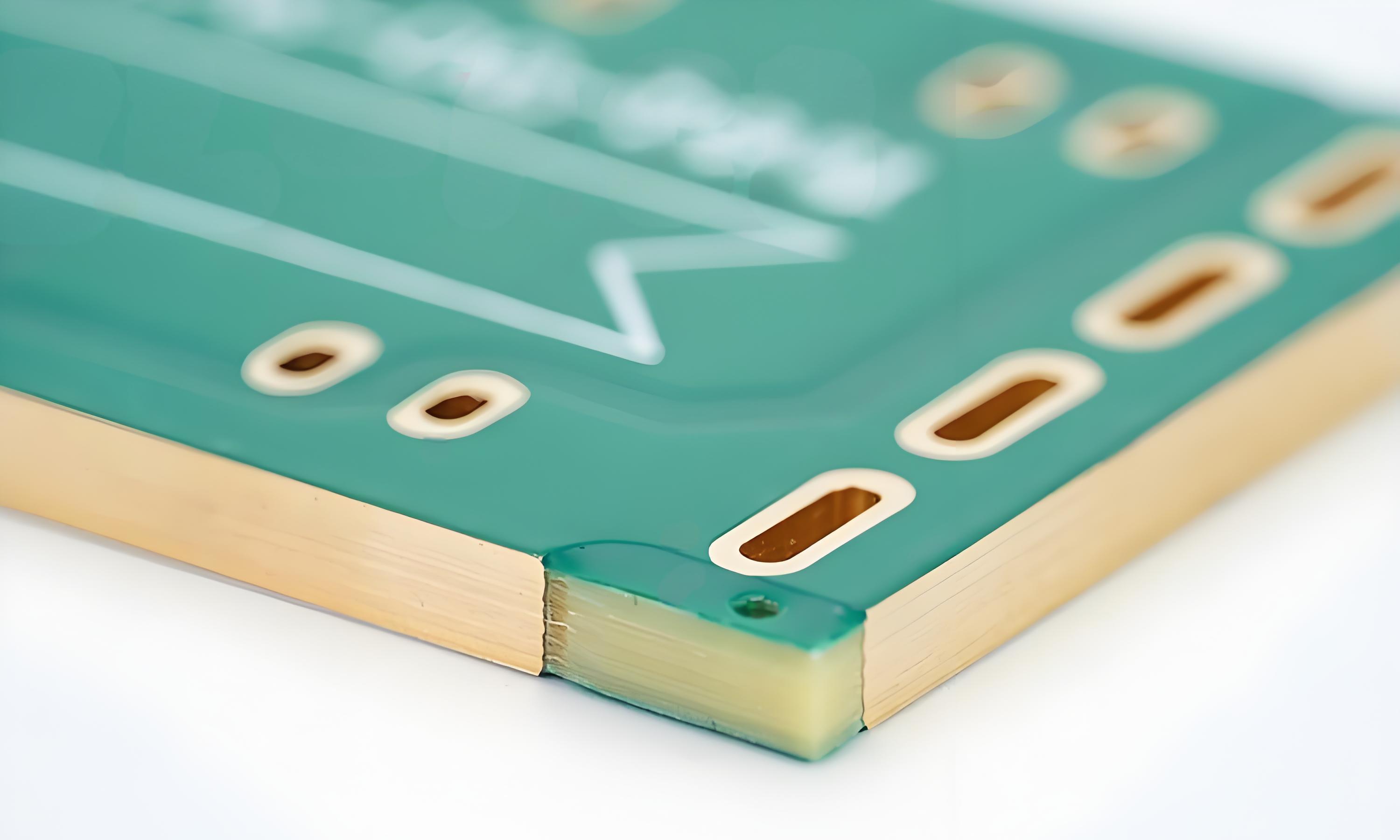
How is a Copper Metal Core PCB Made?
The manufacturing of a copper metal core PCB differs from standard PCB production. It requires precision and advanced techniques.
Step-by-step process:
- Copper sheet selection: High-purity copper sheets are chosen for the core. Purity ensures consistent thermal conductivity.
- Insulation layer application: An insulating dielectric layer is added to separate the copper core from the circuit traces.
- Copper layering: Copper foil is laminated on both sides of the dielectric layer. This creates the circuit paths.
- Etching: The unwanted copper is chemically removed to form the desired circuit design.
- Surface finish: Methods like HASL, ENIG, or immersion silver are applied to protect the copper and improve solderability.
- Testing and inspection: Each board is rigorously tested for electrical continuity, thermal performance, and mechanical stability.
This process ensures that copper core PCBs perform well under high thermal and electrical stress.
Do PCBs Have Copper?
Yes, copper is a standard material in all PCBs. It forms the conductive pathways that carry electricity. Standard FR4 PCBs use copper only in traces and pads.
Copper core PCBs are different. The copper is in the core, not just the circuit layers. This gives them superior heat conduction. Components stay cooler, even under heavy loads.
Copper’s excellent electrical and thermal conductivity ensures stable performance. Devices work reliably for years without overheating.
What Type of Copper is Used in PCB?
The type of copper affects both thermal and electrical performance. In copper core PCBs, BEST Technology typically use:
- High-purity electrolytic copper: Provides consistent conductivity and low resistance.
- Oxygen-free copper (OFC): Reduces oxidation and ensures long-term stability.
- Rolled annealed copper: Offers flexibility and mechanical strength for assembly.
Choosing the right copper type ensures high thermal conductivity, strong mechanical support, and stable electrical performance. This is especially important in LEDs, automotive electronics, and industrial equipment.
The Types of Copper-Based PCB
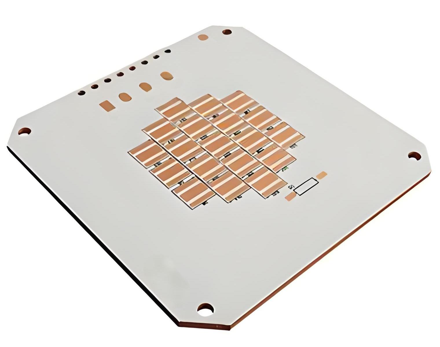
Copper-based PCBs can vary depending on the application. The main types include:
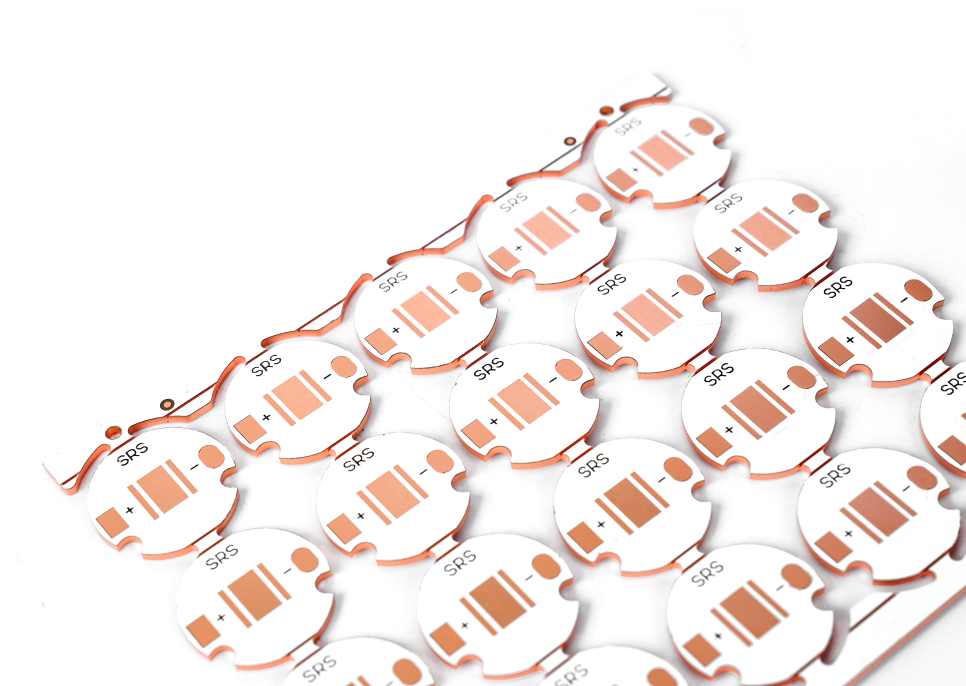
- Single-layer copper core PCB: Features one conductive layer. Often used in simple LED modules or low-power devices.
- Double-layer copper core PCB: Has copper on both sides. This design supports more complex routing while maintaining heat management.
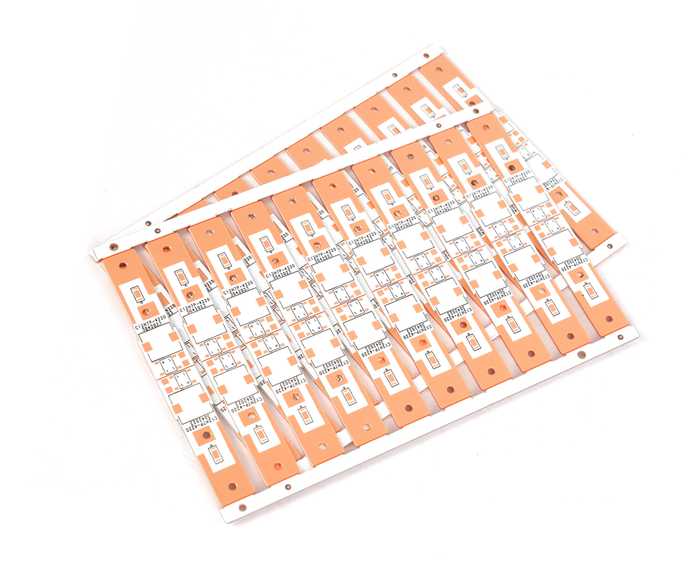
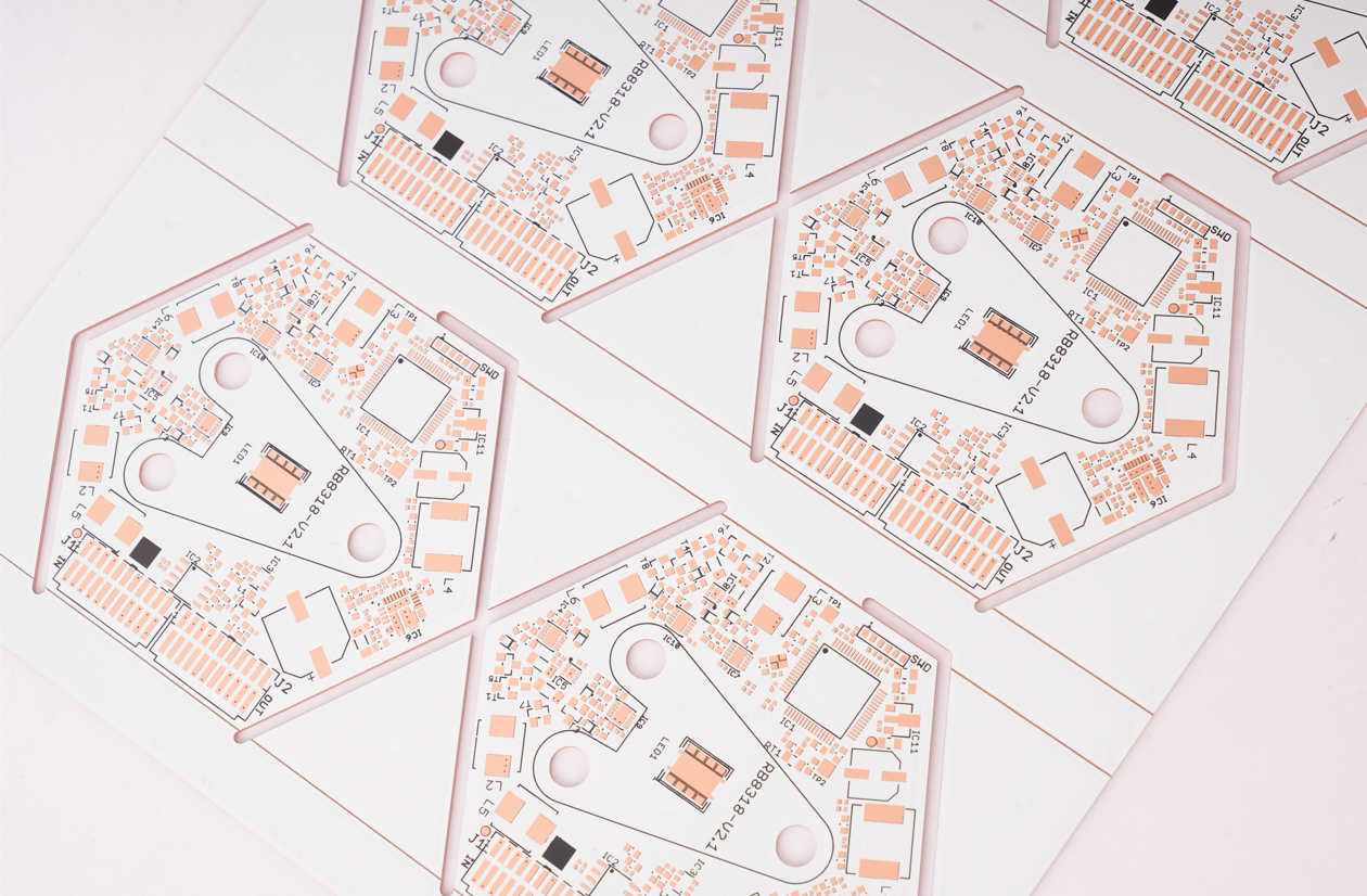
- Multilayer copper core PCB: Includes multiple circuit layers with a central copper core. Ideal for high-power, dense electronics.
- Flexible copper core PCB: Thin copper sheets with flexible substrates allow heat dissipation and adaptable design.
Each type is tailored for specific needs. LEDs often use single or double-layer boards. Industrial and automotive applications prefer multilayer copper core PCBs.
Is Copper Core or Aluminum Core Better?
Both copper and aluminum core PCBs are designed to manage heat efficiently. However, copper offers several advantages.
Advantages of copper core:
- Higher thermal conductivity.
- Better electrical performance.
- Greater long-term reliability.
Advantages of aluminum core:
- Lower cost.
- Lightweight construction.
- Suitable for moderate heat applications.
While aluminum cores are cost-effective, copper core PCBs outperform them in thermal management, reliability, and longevity. This makes copper the preferred choice for high-power and high-reliability electronics.
Copper Core vs Aluminum Core – Thermal Conductivity
Thermal conductivity determines how efficiently a material transfers heat. This is critical in electronics design.
- Copper core PCB: Typically 300–400 W/m·K.
- Aluminum core PCB: Typically 1-30 W/m·K.
Copper conducts heat several times faster than aluminum. This keeps components cooler and prevents hotspots. Electronics run efficiently and last longer when heat is managed properly.
Conclusion:
PCB copper core ensures excellent thermal conductivity. Components stay cool, even under high power or prolonged use. Copper core PCBs are durable, reliable, and suitable for compact designs. Compared to aluminum, they provide higher conductivity, better performance, and longer lifespan.
These boards are widely used in LED lighting, automotive electronics, industrial equipment, and power modules. Choosing a copper core PCB improves efficiency, safety, and product reliability.
For more information or inquiries, contact sales@bestpcbs.com