Alumina substrate thickness is far more than just a dimensional spec. It sits at the heart of your ceramic PCB’s performance, influencing everything from heat management to structural integrity. Getting this thickness right is a fundamental step in designing reliable electronics for demanding applications. This article will walk you through what alumina substrate thickness means, how it compares to other materials, and provide a practical guide to making the best choice for your project.
Have you ever felt stuck when specifying your ceramic PCB? Many engineers face similar hurdles when dealing with alumina substrates.
- Thermal Management Headaches: It’s tricky to balance heat spreading needs with the design’s overall thinness. A thick substrate manages heat well but can limit miniaturization.
- Mechanical Strength Worries: Will the board be robust enough for assembly and its operating environment? Choosing a thickness that is too thin risks fragility and breakage.
- Signal Integrity Challenges: For high-frequency circuits, the substrate thickness directly impacts impedance control. An incorrect choice can lead to signal loss and degraded performance.
- Manufacturing and Cost Pressures: Specific thicknesses can be harder to produce, potentially increasing lead times and costs. It’s a constant battle between ideal performance and practical budget.
- Material Confusion: The differences between alumina types (like regular vs. calcined) and other metal substrates like aluminum can be unclear, making selection difficult.
The good news is that these challenges have clear solutions. As a specialized Ceramic PCB manufacturer, EBest Circuit (Best Technology) focuses on turning these pain points into strengths.
- Expert Thermal Design Support: We provide direct engineering support to model the thermal performance of different alumina substrate thickness options for your specific application.
- Strength and Reliability Testing: Our factory conducts rigorous mechanical tests on various thicknesses. We share this data to help you select a board that is both slim and strong.
- Impedance Control Expertise: For RF and high-speed designs, our engineers help you calculate the optimal alumina substrate thickness to achieve precise impedance matching.
- Optimized Manufacturing for Cost-Effectiveness: We maintain stock of common alumina substrate thicknesses and offer guidance on standard options that deliver performance without unnecessary cost.
- Clarifying Material Properties: We cut through the confusion with clear documentation on the properties of different alumina grades and how they compare to alternative substrates.
At EBest Circuit (Best Technology), we pride ourselves on being more than just a supplier; we are your partner in ceramic PCB solutions. With nearly two decades of experience, our factory is equipped with advanced technology for manufacturing high-quality alumina substrates. We offer comprehensive support, from material selection and design review to prototyping and mass production. If you have any new project in hand, our engineering team is ready to help. Reach out to us at sales@bestpcbs.com to start a discussion.
What is Alumina Substrate Thickness?
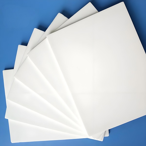
First, an alumina substrate is a thin, flat board made primarily from aluminum oxide (Al₂O₃). It serves as the insulating foundation for building electronic circuits. Unlike standard FR4 PCBs, alumina offers superior thermal conductivity, electrical insulation, and stability in high-temperature environments. The “thickness” refers to the distance between its top and bottom surfaces, a key factor determining its capabilities.
To understand this better, it helps to know about thin films. In electronics, a “thin film” is a layer of material deposited on the substrate, often measured in micrometers or even nanometers. For instance, the conductive traces on a substrate are a type of thin film. The substrate itself is much thicker, providing the mechanical backbone. While a thin film might be 10 micrometers thick, the alumina substrate supporting it typically ranges from 0.25mm to over 1.0mm.
- For comparison, a common standard thickness for FR4 substrates is 1.6mm.
- Alumina substrates, however, are often used in thinner profiles because of their inherent strength and excellent heat dissipation.
This allows for more compact and efficient designs. So, when we talk about alumina substrate thickness, we’re discussing a critical design lever that balances mechanical support, thermal performance, and electrical characteristics.
What Is the Difference Between Alumina and Calcined Alumina?
This is a common point of confusion. The key difference lies in the processing stage and purity.
- Alumina (Aluminum Oxide): This is the general term for the chemical compound Al₂O₃. In the context of substrates, it refers to a fully processed, high-purity ceramic material. It has been sintered at high temperatures to form a dense, strong, and stable solid.
- Calcined Alumina: This is an intermediate product. It is alumina that has been heated (calcined) to remove volatile impurities and convert it to a more stable oxide form, but it has not yet been sintered into a final, dense body. It is typically a powder.
Think of it this way: calcined alumina is the high-quality raw material, while the finished alumina substrate is the final product. Substrate manufacturers use calcined alumina powder, mix it with binders, shape it, and then fire it at high temperatures. This sintering process creates the strong, cohesive ceramic board we use for PCBs. Therefore, the alumina in your PCB is a fully sintered, high-purity ceramic, not the calcined powder.
What Is the Difference Between Al₂O₃ Substrate and Aluminium Substrate?
While both contain aluminum, they are fundamentally different materials designed for different jobs. An Al2O3 substrate (alumina ceramic) is an electrical insulator. Its primary role is to support circuit traces and manage heat while preventing electrical shorts. It is ideal for high-frequency, high-power, and high-temperature applications where superior insulation and thermal stability are non-negotiable.
An aluminum substrate (also called a metal-clad or IMS board) is essentially a thermal conductor. It is a metal core—usually aluminum—coated with a thin layer of dielectric polymer and then a copper layer. Its main job is to draw heat away from components very effectively, but its electrical insulation is provided by the thin polymer layer, which has limits on voltage and temperature.
Here’s a quick comparison:
| Feature | Al2O3 Substrate (Ceramic) | Aluminum Substrate (Metal-Clad) |
|---|---|---|
| Core Material | Aluminum Oxide (Ceramic) | Aluminum Metal |
| Electrical Insulation | Excellent (Bulk material property) | Good (From a thin polymer layer) |
| Thermal Conductivity | Good (24-28 W/mK) | Very Good (1-3 W/mK for the entire board) |
| Max Operating Temp | Very High (>350°C) | Moderate (typically 130-150°C) |
| Primary Use | High-frequency/RF, harsh environments, high reliability | LED lighting, power supplies, where cost-effective cooling is key |
What Are the Pros and Cons of Al₂O₃ Substrate?
Alumina substrates offer a compelling set of advantages but also come with some trade-offs.
Pros:
- Excellent Electrical Insulation: Its high dielectric strength makes it perfect for high-voltage and high-frequency applications.
- Good Thermal Conductivity: With a typical range of 24-28 W/mK, it effectively draws heat away from sensitive components, improving longevity.
- High Mechanical Strength: Alumina is a rigid and hard material, offering great resistance to wear and abrasion.
- Superior Thermal Stability: It has a very high melting point and can withstand high-temperature processing and operating environments without deforming.
- Chemical Resistance: It is inert to most chemicals and moisture, ensuring long-term reliability.
Cons:
- Brittleness: Unlike FR4 or metal cores, alumina is a ceramic and can be brittle, making it susceptible to cracking under sharp impact or flexing.
- Higher Cost: The raw material and manufacturing processes are more expensive than standard PCB materials like FR4.
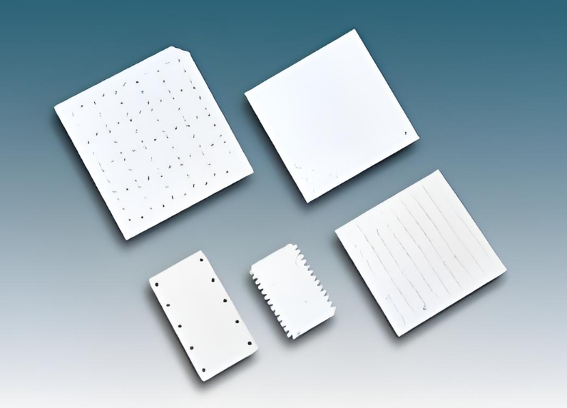
- Harder to Machine: Drilling and cutting require specialized laser equipment, which adds to the cost and complexity compared to standard PCB routing.
- Heavier Weight: It is denser than polymer-based substrates, which might be a concern for weight-sensitive applications.
How to Choose Alumina Substrate Thickness?
Selecting the right alumina substrate thickness is a balancing act. There is no one-size-fits-all answer. The best choice depends on your project’s specific priorities. Here is a practical framework to guide your decision, focusing on four key areas.
1. Prioritize Thermal Performance
- The primary reason for choosing alumina is often thermal management. Thicker substrates have a greater thermal mass and a lower thermal resistance for spreading heat laterally. If your main goal is to keep a high-power component cool, a thicker substrate (e.g., 0.635mm or 1.0mm) is generally better. It acts as a more effective heat spreader. For example, a 1.0mm substrate can be about 30% more effective at lateral heat spreading than a 0.25mm substrate, reducing hot spots.
2. Ensure Mechanical Stability
- The substrate must be robust enough to survive assembly (handling, component placement, soldering) and its operational life. Thinner substrates (e.g., 0.25mm) are more fragile and can warp or crack during processing. For larger boards or those used in high-vibration environments, a thicker substrate (e.g., 0.635mm or more) provides crucial rigidity and strength. A simple rule: the larger the board area, the thicker it should be for mechanical integrity.
3. Meet Electrical Requirements
- For high-frequency circuits, the substrate thickness is critical for controlling impedance. The characteristic impedance of a microstrip line depends on the trace width and the substrate thickness. A standard formula for approximation is:
Z₀ ≈ (87 / √(ε_r + 1.41)) * ln(5.98H / (0.8W + T))
Where Z₀ is impedance, ε_r is the dielectric constant (~9.8 for alumina), H is the substrate thickness, W is the trace width, and T is the trace thickness. To achieve a specific impedance (e.g., 50Ω), you need to carefully coordinate trace width and substrate thickness. Thinner substrates allow for finer, more controlled impedance lines but are harder to manufacture with thick metal layers.
4. Consider Manufacturing and Cost
- Finally, consider practicality. Standard thicknesses like 0.25mm, 0.38mm, 0.635mm, and 1.0mm are more readily available and cost-effective. Opting for an unusual, custom thickness can significantly increase cost and lead time. Furthermore, the chosen thickness must be compatible with the desired metalization thickness. Thick-film printing on very thin substrates can be challenging. Always discuss your requirements with your manufacturer early on.
Case of Alumina Substrate PCB Manufactured by EBest Circuit (Best Technology)
A recent project for a automotive sensor module perfectly illustrates the importance of thickness selection. The client needed a small, robust board for a high-temperature environment near an engine. The board had to manage heat from a dedicated IC and maintain stable performance under vibration.
We recommended an Al2O3 substrate with a thickness of 0.635mm. This choice struck an ideal balance:
- Thermally, it was thick enough to effectively spread the localized heat from the IC.
- Mechanically, it provided the necessary strength to prevent cracking during assembly and under engine vibration, something a thinner 0.25mm board might not have survived.
- Electrically, it allowed for the precise trace widths needed for stable sensor signals.
The result was a highly reliable PCB that met all the client’s stringent automotive requirements. This case shows how a targeted thickness choice, backed by experience, leads to a successful product.
Why Choose EBest Circuit (Best Technology) for Alumina Substrate PCB Solution?
Selecting the right partner is as important as selecting the right thickness. EBest Circuit (Best Technology) brings distinct advantages to your project. Our deep expertise in ceramic PCB manufacturing allows us to guide you through the complexities of material and thickness selection.
- Full Technical Guidance: We provide more than just manufacturing. Our engineering team works directly with you, offering expert guidance on material selection and design optimization to ensure your alumina substrate PCB meets all performance and reliability goals.
- Advanced Manufacturing and Rigorous Inspection: Our factory is equipped with advanced laser processing and inspection systems. This ensures every alumina substrate we produce meets precise dimensional and quality standards, guaranteeing consistency and high yield.
- Comprehensive Thickness and Material Options: We offer a wide range of standard and custom alumina substrate thickness options. Each option is supported by thorough engineering analysis to ensure your design is not only functional but also optimized for manufacturability.
- Proven Supply Chain and Material Stability: We maintain strong partnerships with leading raw material suppliers. This ensures consistent access to high-quality alumina powders, guaranteeing the stability and reliability of your PCBs from prototype through mass production.
- End-to-End Quality and Traceability: We implement a full-process quality management system. From incoming material inspection to final shipment, every step is documented, providing complete traceability for applications requiring the highest levels of quality assurance.
Partnering with EBest Circuit (Best Technology) for your alumina substrate PCB needs means gaining more than just a supplier. Our combination of engineering expertise, advanced manufacturing capabilities, and a customer-focused approach ensures that your projects are built on a solid foundation, enabling you to achieve success in the most demanding applications.
In summary, alumina substrate thickness is a fundamental choice that directly shapes the success of your high-performance electronics. It influences thermal management, structural integrity, and electrical behavior. By understanding the properties of alumina and carefully weighing the factors of thermal needs, mechanical stability, electrical requirements, and cost, you can make a confident and optimal decision.
At EBest Circuit (Best Technology), we are committed to helping you navigate these choices. Our team provides the technical support and manufacturing excellence needed to bring your most challenging designs to life. If you are working on a project that could benefit from our expertise in alumina substrates, please contact us at sales@bestpcbs.com.