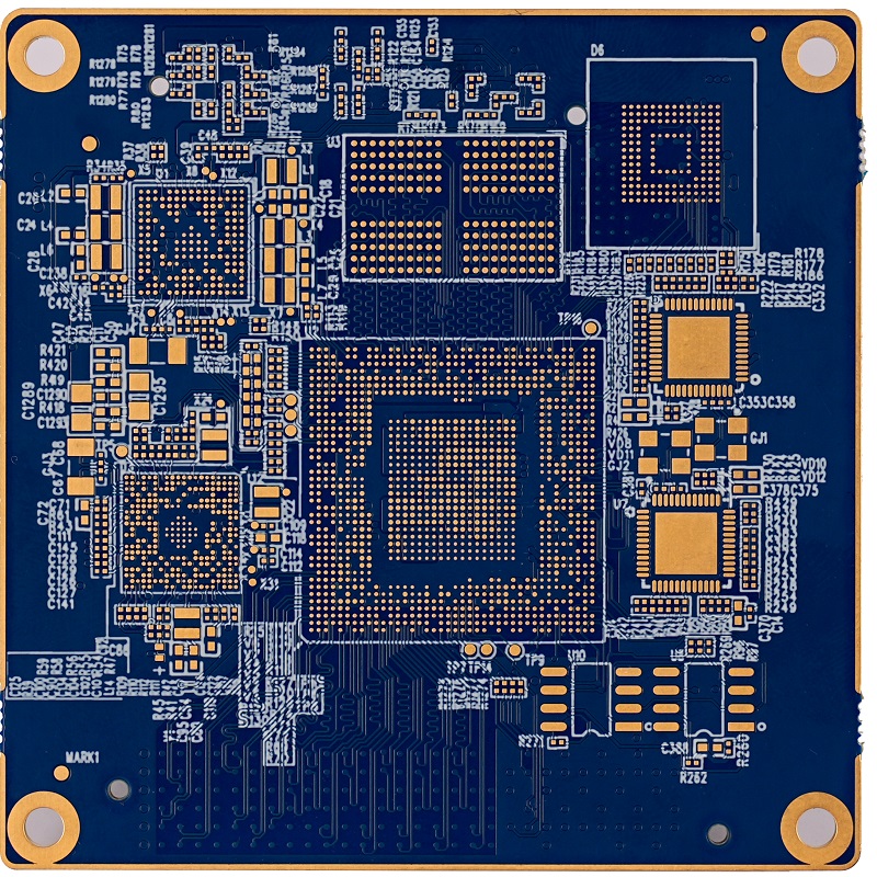
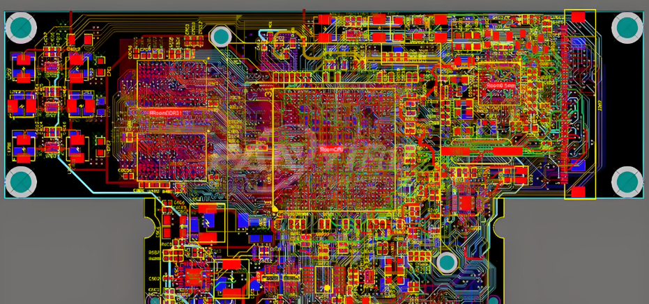
Designing a reliable multilayer circuit board starts with getting the stackup right. If your project involves high-speed signals, compact layouts, or reduced EMI, an 8-layer PCB stackup is a solid choice. It offers flexibility, better performance, and room for complex routing.
In this guide, we’ll walk you through everything you need to know—layer configurations, materials, sizes, and how to make the most of this structure with the help of a trusted PCB manufacturer.
What is a PCB Stackup?
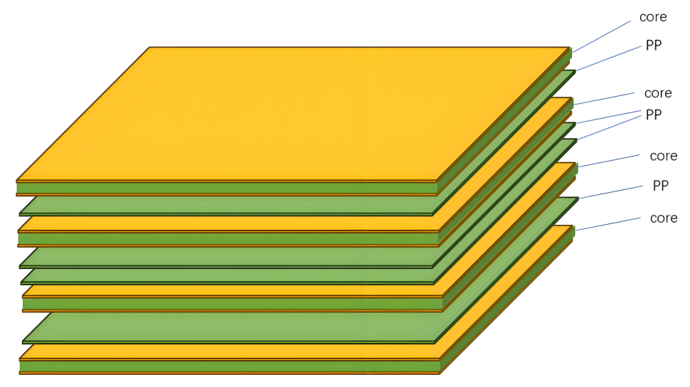
A PCB stackup is the arrangement of copper layers and insulating materials inside a circuit board. These layers are stacked and bonded together using prepreg (resin-impregnated fiberglass) and core materials. The goal is to create a reliable board that supports both mechanical strength and excellent electrical performance.
In simple words, the stackup decides how signal layers, power planes, and ground layers are placed in the board. In high-speed digital designs, this structure plays a big role in signal quality, electromagnetic compatibility (EMC), and overall performance.
For an 8-layer PCB, the stackup consists of eight layers of copper with alternating dielectric materials. These are usually divided into four signal layers and four plane layers, though that can change based on your design needs.
PCB Stackup Considerations
For most PCB designs, there are often competing requirements between electrical performance, manufacturing limitations, cost targets, and system complexity. The final PCB stackup is usually a result of careful trade-offs across these factors. High-speed digital circuits and RF systems commonly rely on multilayer boards for better control and performance. Below are 8 essential principles to consider when designing a reliable stackup:
1. Layer Arrangement
In multilayer PCBs, you’ll typically work with signal layers (S), power planes (P), and ground planes (GND). Power and ground planes are usually solid, unbroken areas that provide low-impedance return paths for signal currents. Signal layers are often positioned between these planes to form symmetrical or asymmetrical stripline structures. The top and bottom layers are mainly used for component placement and limited routing. It’s best to keep traces on these outer layers short to reduce direct radiation and EMI.
2. Defining a Single Power Reference Plane
Decoupling capacitors are vital for maintaining power integrity, and they can only be placed on the outer layers of the PCB. The trace length, pad design, and vias connected to these capacitors greatly affect their effectiveness. To improve decoupling, make these connections short and wide, and minimize via length. For example, in a high-speed digital system, place decoupling capacitors on the top layer, dedicate the second layer to power for the processor, use the third layer for signal routing, and assign the fourth layer as a ground reference.
3. Incorporating Multiple Ground Planes
Using multiple ground planes helps create low-impedance return paths and minimizes common-mode EMI. Ground and power planes should be tightly coupled, and signal layers should also be close to reference planes. Reducing the dielectric thickness between layers improves coupling and enhances performance.
4. Managing Multiple Power Planes
When your design includes more than one power plane, these planes are often split into different voltage regions. If a signal layer is placed next to a multi-region power layer, signal currents may not find clean return paths, leading to noise or EMC issues. For high-speed digital signals, avoid routing traces near split power planes to prevent return current discontinuities.
5. Designing Signal Routing Pairs
When a signal travels from one layer to another, it creates what’s known as a “routing pair.” Ideally, the return current should stay within the same reference plane when switching layers. In practice, however, signals often need to transition between layers. To maintain signal integrity, ensure that return paths are available through stitching vias or decoupling capacitors. Using adjacent layers as routing pairs is a practical and effective strategy.
6. Routing Direction Guidelines
Keep trace directions consistent within each signal layer. At the same time, rotate the routing direction between adjacent signal layers. For instance, use horizontal routing (X-axis) on one layer and vertical routing (Y-axis) on the next. This practice reduces crosstalk and improves signal clarity.
7. Even-Layer Designs is Better
Although odd-layer PCBs may appear cheaper due to fewer materials, they’re more expensive to manufacture. That’s because odd-layer boards require non-standard lamination processes and additional handling steps. These increase the risk of surface damage, incorrect etching, and longer production times. In contrast, even-layer PCBs are more stable, cost-effective, and easier to produce at scale.
8. Budget
Multilayer PCBs are naturally more expensive than single- or double-layer boards. However, they offer significant benefits in functionality, miniaturization, EMI control, and signal integrity. When weighing total cost versus performance, the difference between multilayer and simpler boards may not be as high as expected.
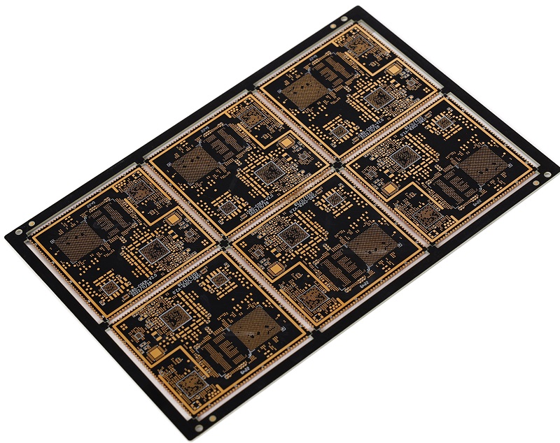
Standard 8-Layer PCB Stackup Structure
When it comes to multilayer PCB design, the arrangement of signal, power, and ground layers directly affects signal integrity, EMI performance, and power delivery. Below are three common 8-layer stackup configurations, each with its own strengths and limitations.
Option 1:
Layer 1: Signal 1
Layer 2: Signal 2
Layer 3: Ground
Layer 4: Signal 3
Layer 5: Signal 4
Layer 6: Power
Layer 7: Signal 5
Layer 8: Signal 6
This layout alternates signal and power layers but does not take full advantage of the electromagnetic shielding benefits that a multilayer board can offer. The ground and power planes are separated, reducing the board’s EMI suppression capability. In addition, the power distribution network suffers from higher impedance, which may affect voltage stability in high-speed or high-current applications.
Option 2:
Layer 1: Signal 1
Layer 2: Ground
Layer 3: Signal 2
Layer 4: Power
Layer 5: Ground
Layer 6: Signal 3
Layer 7: Ground
Layer 8: Signal 4
This structure is widely regarded as the optimal 8-layer PCB stackup. It provides excellent electromagnetic shielding through the use of multiple ground planes. Each signal layer is placed adjacent to a reference plane (either ground or power), which improves signal stability and impedance control. Additionally, the tight coupling between power and ground planes enhances EMI performance and power integrity. This setup is ideal for high-speed, high-frequency, or noise-sensitive applications.
Option 3:
Layer 1: Signal 1
Layer 2: Ground
Layer 3: Signal 2
Layer 4: Power
Layer 5: Ground
Layer 6: Signal 3
Layer 7: Power
Layer 8: Signal 4
This configuration is a variation of Option 1 with improved EMI performance. By adding an extra reference plane, it provides better control over the characteristic impedance of the signal layers. However, the placement of the second power plane (with limited coupling to a nearby ground) leads to higher power delivery impedance, which could be a drawback in power-sensitive designs. Some optimization in power layer arrangement is still needed.
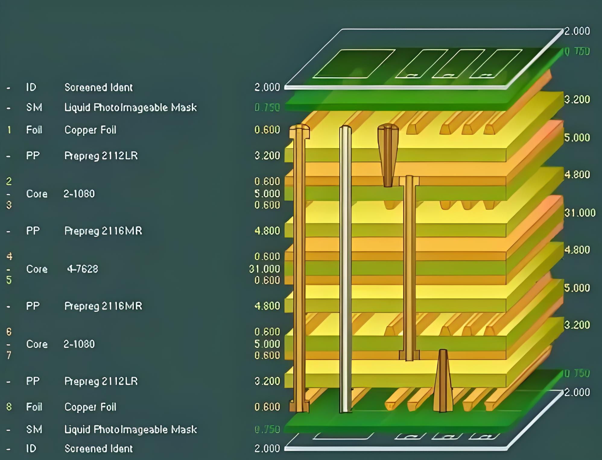
8-Layer PCB Stackup Materials
The performance of an 8-layer PCB stackup relies heavily on the materials used between and around its copper layers. These materials affect everything from electrical behavior to thermal stability and even mechanical strength. Let’s look at the two main categories: conductive and dielectric materials.
1. Conductive Layers
Copper is the most common metal used for the conductive layers in an 8-layer PCB. It’s highly conductive, easy to work with, and available in different thicknesses and finishes.
- Copper Thickness: Most boards use ½ oz or 1 oz copper per layer. If the design needs to handle higher current, 2 oz or thicker copper may be used.
- Copper Type: Standard copper foil is either electrodeposited (ED) or rolled. Rolled and annealed copper is smoother and more flexible, which makes it useful in boards that need better bend resistance.
- Surface Finishes: The exposed copper is usually treated with a surface finish to protect it and ensure solderability. Options include HASL, ENIG, OSP, and immersion silver, among others.
2. Dielectric Layers
The dielectric materials are the insulating layers that separate the copper traces. These layers are critical for controlling impedance, heat flow, and electrical isolation.
- FR-4: A glass-reinforced epoxy laminate, FR-4 is the most common dielectric for general-purpose PCBs. It’s reliable, widely available, and cost-effective.
- High-Frequency Materials: For RF and high-speed digital designs, materials with low dielectric loss—like PTFE (Teflon), ceramic-filled PTFE, or hydrocarbon-based ceramics—are preferred. These support better signal integrity at high frequencies.
- Thermal Conductive Materials: When heat dissipation is a concern, substrates like alumina or aluminum nitride are used. These materials offer higher thermal conductivity than standard epoxy systems.
To hold everything together, manufacturers use prepregs—uncured fiberglass sheets soaked in resin. Common prepreg materials include FR-4 for standard designs and polyimide for higher thermal or mechanical stress environments.
At the center of the stackup is the core, which acts like a spine for the board. This rigid layer typically uses FR-4 or polyimide, though in some high-power or high-heat applications, metal cores are added to improve thermal performance.
8-Layer PCB Thickness & Sizes
The total thickness of an 8-layer PCB depends on several factors:
- Copper thickness: Common values are 0.5oz, 1oz, or 2oz per layer.
- Prepreg/Core thickness: Adjusted to achieve specific impedance and board height.
- Number of plane vs signal layers: Affects thermal and mechanical behavior.
Common Thickness Options:
- 1.6mm (0.063″) – Industry standard, suitable for most applications.
- 2.0mm to 2.4mm – Used when extra copper is needed for higher current.
- 3.2mm or custom – Selected for industrial or military-grade boards.
PCB Sizes:
Panel sizes are typically 18” x 24” before routing. Your board can be as small as a few millimeters or as large as the full panel, depending on the application.
6 Layer vs 8 Layer PCB
A 6-layer PCB consists of six layers of copper circuitry stacked with insulating layers (prepreg and core) in between. It usually includes:
- 4 Signal Layers for routing high- and low-speed signals
- 1 Power Plane to distribute voltage
- 1 Ground Plane to provide a return path and help with EMI suppression
A typical 6-layer stackup looks like this:
Layer 1: Signal (Top)
Layer 2: Ground
Layer 3: Signal
Layer 4: Signal
Layer 5: Power
Layer 6: Signal (Bottom)
While both 6-layer and 8-layer PCBs are widely used in advanced electronics, they serve slightly different purposes depending on design complexity, signal speed, and EMI requirements. Let’s compare them together:
| Aspect | 6-Layer PCB | 8-Layer PCB |
| Layer Count | 6 | 8 |
| Typical Configuration | 4 signal layers + 1 power + 1 ground | 4 signal layers + 2 power + 2 ground |
| Routing Space | Moderate | More routing room |
| Signal Integrity | Good, suitable for most mid-speed signals | Excellent, supports very high-speed signal routing |
| EMI Shielding | Limited shielding with fewer ground planes | Strong EMI control due to multiple ground planes |
| Power Distribution | Single power plane, higher impedance | Dual power planes, better PDN performance |
| Design Complexity | Less complex, easier to design and fabricate | More complex, better for advanced designs |
| Thermal Performance | Adequate for medium power applications | Better heat spreading for high-power components |
| Cost | Lower fabrication cost | Higher cost due to more layers and materials |
| Use Case | Mid-level MCUs, general embedded, basic RF | FPGAs, DDR memory, high-speed data buses, complex SoCs |
Use a 6-Layer PCB if:
- Your design isn’t extremely dense.
- The signals don’t require tight EMI control.
- You want to balance performance and cost.
- There’s no strict need for multiple ground or power planes.
It’s widely used in commercial electronics that don’t involve ultra-high-speed communication or compact multilayer routing challenges.
Choose an 8-Layer PCB when:
- High-speed signals (such as PCIe, USB 3.x, DDR4, or SERDES) are involved.
- EMI performance is critical, especially in sensitive industrial or medical devices.
- You need more space for routing due to a denser component layout.
- Stable power delivery is required across multiple voltage domains.
- You’re working with a compact form factor that demands vertical signal distribution.
An 8-layer stackup allows designers to pair every signal layer with a nearby ground or power plane, which significantly improves signal quality and reduces noise.
Benefits of Working with an Experienced PCB Manufacturer
Designing and fabricating an 8-layer PCB stackup requires precise engineering and process control. Partnering with a reliable manufacturer like EBest Circuit (Best Technology) brings several benefits:
1. Stackup Design Assistance: Professional help with impedance control, signal integrity, and EMC optimization.
2. Material Expertise: Guidance in choosing suitable laminates for your specific requirements.
3. Advanced Fabrication: Capability to handle HDI, blind/buried vias, and tight tolerances.
4. Quality Assurance: Rigorous testing like AOI, X-ray, and impedance measurement.
5. Fast Turnaround: Efficient production process without sacrificing quality.
Why Choose EBest Circuit (Best Technology) for Your 8-Layer PCB Stackup?
EBest Circuit (Best Technology) is a trusted 8-layer PCB stackup specialist serving global customers across aerospace, medical, automotive, and industrial electronics. We hold certifications including:
- ISO9001 for quality control
- ISO13485 for medical electronics
- IATF16949 for automotive-grade PCBs
- AS9100D for aerospace applications
Our engineers assist with DFM check, impedance control, EMI reduction, thermal management, and material choices, ensuring your 8-layer design performs reliably under real-world conditions.
FAQs
1. What is the best layer configuration for an 8-layer PCB stackup?
A balanced configuration like Signal–GND–Signal–Power–GND–Signal–Power–Signal is often preferred for signal integrity and EMI control.
2. How much does an 8-layer PCB cost?
Cost varies by material, size, copper weight, and complexity, but typically ranges from $50 to $300 per board in small batches.
3. What software is used for 8-layer PCB design?
Tools like Altium Designer, Eagle, KiCAD, and OrCAD support multilayer PCB stackup planning and layout.
4. Can you use HDI features in 8-layer PCBs?
Yes. Blind and buried vias, via-in-pad, and microvias are often used in 8-layer HDI designs.
5. How do I choose the right manufacturer for 8-layer PCBs?
Look for certifications, material options, engineering support, and experience with multilayer stackups—like what EBest Circuit (Best Technology) provides.