Looking for medical PCBA manufacturer? This blog will explain its standards, manufacturing processes, and service types, and demonstrate how EBest Circuit (Best Technology), as a leading ISO 13485 certified manufacturer in China, provides reliable solutions.
Are you troubled these following issues with medical PCBA?
- How can PCB supply chains ensure one-time pass for lengthy medical certification cycles?
- How to ensure long-term stability and no drift of PCBs for high-precision in-vitro diagnostic signals?
- What special requirements do implantable devices have for biocompatible materials and miniaturization processes?
As a professional medical PCBA manufacturer, EBest Circuit (Best Technology) can provide you service and solutions:
- Full-process compliance support: ISO13485/GMP certification package plus technical documentation collaboration to ensure end-to-end compliance from design to production.
- Signal precision assurance: 4-wire differential impedance control, high-Tg substrates, and ENIG finishing to achieve ±1% impedance accuracy, ensuring stable oxygen saturation and ECG signals.
- Miniaturized biocompatible solutions: Biocompatible FR4 substrates and low-temperature co-fired ceramic technology, paired with 01005 ultra-precision placement, to meet long-term stability and miniaturization needs of implantable devices.
Welcome to contact us if you have any inquiry for medical PCBA: sales@bestpcbs.com.
What Is Medical PCBA?
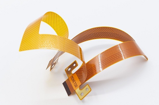
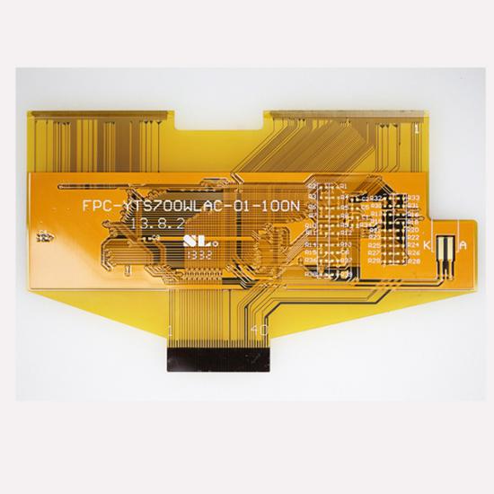
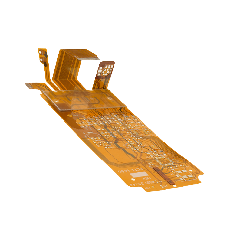
Medical PCBA (Medical Printed Circuit Board Assembly) is a functional circuit system in medical devices where electronic components (such as resistors, capacitors, and IC chips) are integrated onto a medical PCB (printed circuit board) through soldering. Its core characteristics include strict adherence to medical industry certification standards (such as ISO 13485) to ensure quality, safety, and biocompatibility, requiring special treatments such as sterilization and moisture protection (e.g., conformal coating).
Applications of Medical PCB Assembly
- Imaging equipment (CT, MRI), electrophysiological monitoring equipment (ECG, EMG), blood analyzers, etc.
- Pacemakers, neurostimulators, ventilators, blood glucose meters, blood pressure/temperature monitors.
- Implantable cardiac devices, deep brain stimulators, cochlear implants.
- Wearable medical devices (such as smart bracelets), Internet of Things for Medical Technology (IoMT) terminals, medical aesthetic devices.
Medical PCB Assembly Standards & Requirements
ISO 13485:2016
- Requirements: A quality management system covering the entire lifecycle of medical devices, including PCB design, procurement, assembly, and testing. Ensure suppliers have traceable process control capabilities to reduce equipment failure risks and support CE marking and FDA audits.
ISO 9001:2015
- Requirements: A general quality management framework emphasizing continuous improvement and customer satisfaction, applied in conjunction with ISO 13485. Ensure consistency in mass production and reduce the probability of recalls due to process variations.
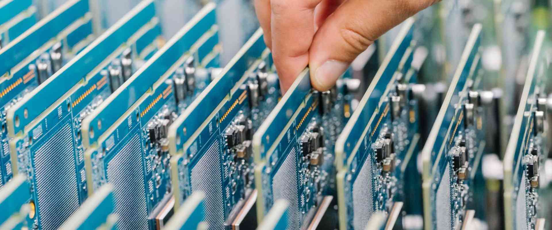
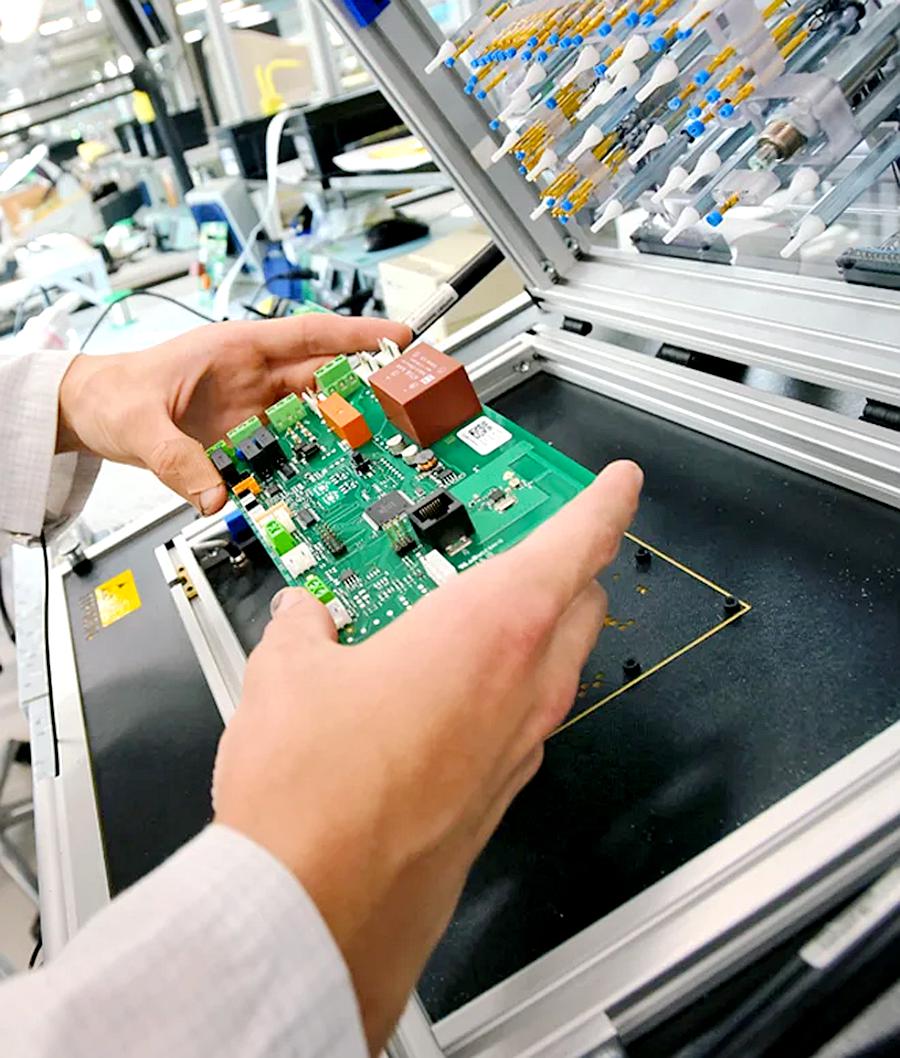
Medical PCB Assembly Manufacturing Process
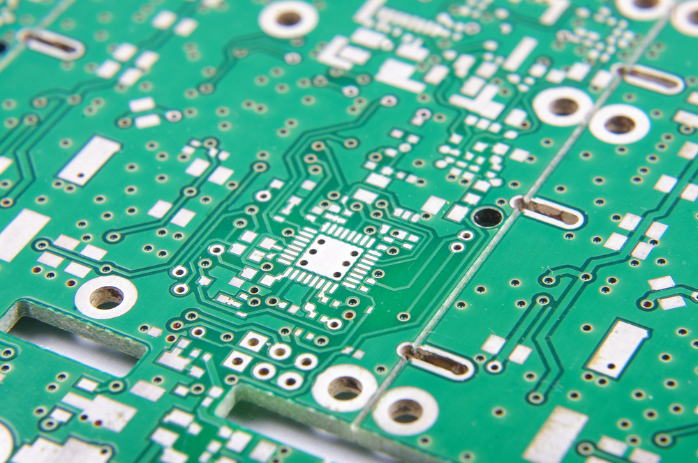
1. Design Verification and DFM Analysis
- Circuit Design: Utilize Altium Designer/Cadence tools to complete medical-grade circuit design, prioritizing EMC compliance, signal integrity (e.g., differential routing, 3W rule), and thermal management.
- DFM Validation: Generate SMT coordinates from Gerber files and BOM lists. Validate manufacturability metrics including line width accuracy (±0.02mm), hole position accuracy (±0.01mm), and layer-to-layer alignment (multilaminate thickness tolerance ±5%).
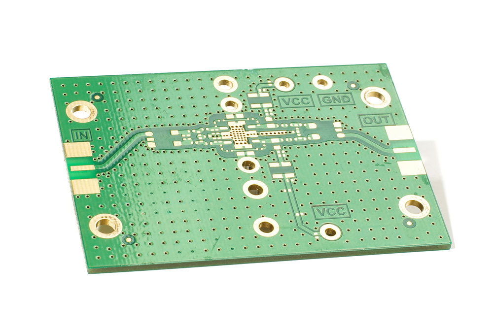
2. Bare PCB Fabrication
Substrate Selection: Prefer high-Tg (≥170℃) halogen-free substrates meeting IEC 61249-2-21 environmental standards, with CTE ≤13ppm/℃ (X/Y directions).
Process Control:
- Etching precision ±0.02mm; edge roughness Ra≤0.5μm.
- Multilaminate lamination via stepwise heating (120℃→150℃→180℃) at 25–30kg/cm² pressure, ensuring interlayer bonding strength ≥1.5N/mm.
- Drilling hole position deviation ±0.01mm; chemical copper plating thickness ≥0.5μm on hole walls.
Surface Finish: Immersion gold (Au 0.8–1.2μm/Ni 5–8μm) or hot-air solder leveling (SAC305 lead-free solder) for solder pad wetting angle ≤30° and 48-hour salt spray resistance.
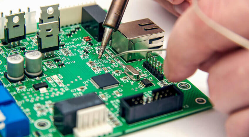
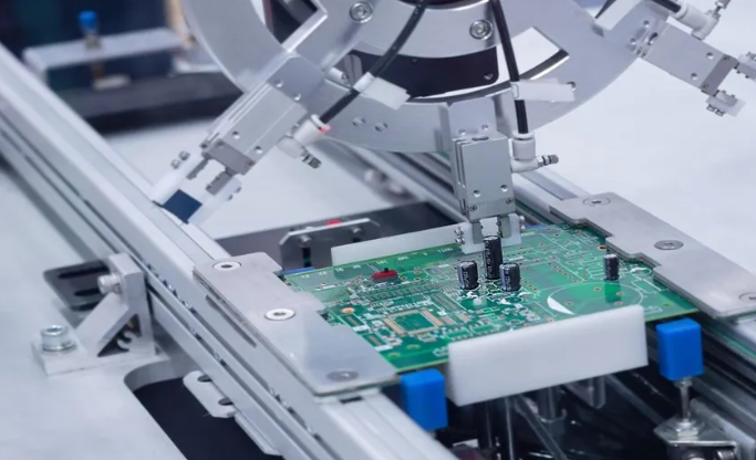
3. SMT Placement and Reflow Soldering
Placement Accuracy: High-precision pick-and-place machines (error ≤0.01mm) for sensitive components (e.g., crystals, microcontrollers).
Solder Paste Printing: Laser-cut stencil printing with uniform paste thickness (±10%) to prevent bridging/solder balls.
Reflow Control:
- Temperature profiling: Preheat 80–120℃ (1–2℃/s ramp), soak 120–150℃, peak 230–250℃ (240±5℃ for 30–60s), cooling 2–3℃/s.
- Nitrogen atmosphere (≥99.99% purity) to reduce solder voids (≤5%) and achieve ≥99.8% soldering yield.
- Sensitive component protection: Kapton tape masking for crystals to prevent thermal damage.
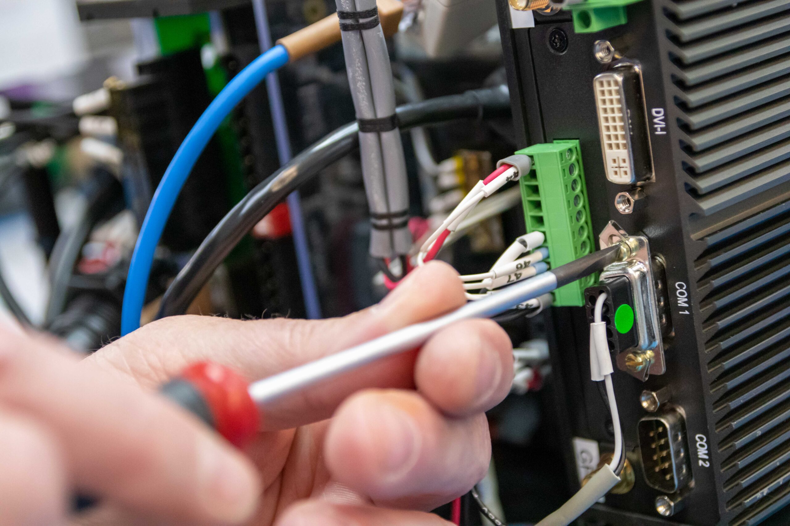
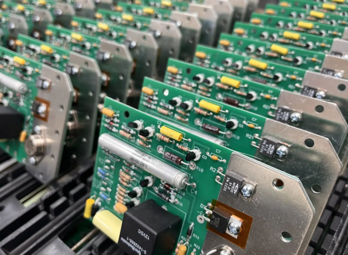
4. DIP Insertion and Wave Soldering
- Insertion Process: Manual insertion for through-hole components (e.g., connectors, electrolytic capacitors). Wave soldering temperature 250–260℃ with cooling rate 2–3℃/s.
- Solder Joint Inspection: AOI + X-ray testing for joint integrity verification, void-free soldering, and ≤10% void rate in critical joints.
5. Testing and Validation
- Electrical Testing: ICT (continuity/isolation), FCT (signal integrity/timing), and burn-in (85℃/85%RH for 1000 hours).
- EMC Testing: Compliance with IEC 60601-1-2 for conducted/radiated emissions; ESD immunity ≥8kV.
- Environmental Testing: Thermal cycling (-40℃~85℃ for 1000 cycles), salt spray (48 hours), vibration (IEC 60068-2).
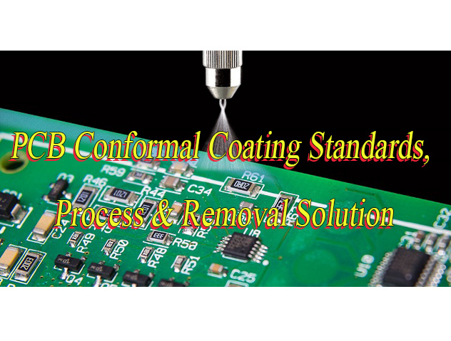
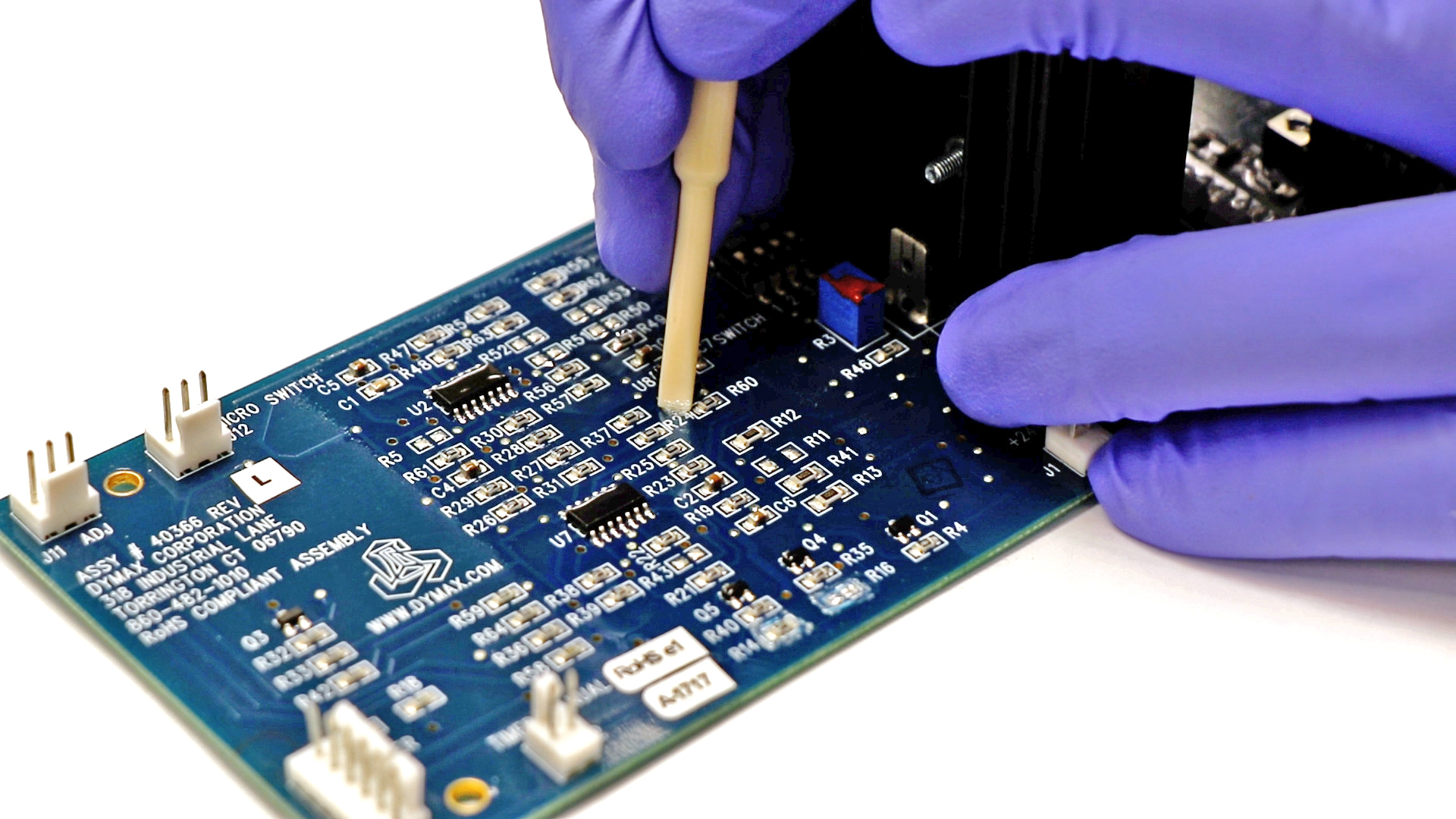
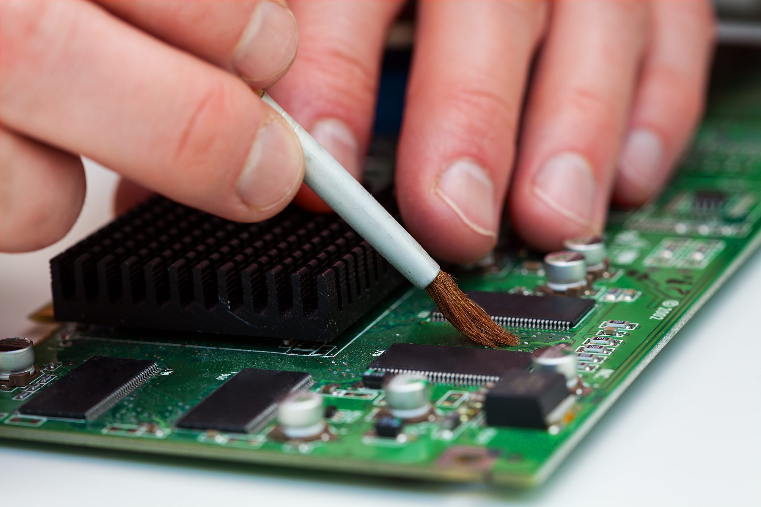
6. Cleaning and Coating
- Cleaning Process: Ultrasonic cleaning to remove flux residues (VOC≤10mg/m³), followed by deionized water rinsing and drying.
- Protective Coating: Biocompatible Parylene-C (2–5μm) or silicone encapsulation for moisture/corrosion resistance. Sterile packaging requires microbial load ≤10CFU/cm².
7. Packaging and Traceability
- Sterile Packaging: Vacuum packaging + nitrogen flushing with EO/gamma sterilization for ≥3-year shelf life.
- Traceability System: Batch tracking of substrates, process parameters, and test data per FDA 21 CFR Part 820 for end-to-end traceability.
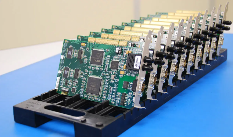
Types of Medical PCB Assembly Service We Can Offer
- Medical PCBA Rapid Prototyping: Supports iterative testing in the early stages of medical device R&D, shortening the cycle from design to functional prototype and meeting the high innovation efficiency requirements of international clients.
- Small-Batch Customized Medical PCBA Production: Provides flexible assembly solutions for low-volume needs in clinical trials or customized medical devices, complying with ISO 13485 and client technical specifications.
- Large-Batch Standardized Medical PCBA Production: Achieves high-precision mass production through automated production lines, meeting the cost control and delivery timeliness requirements of large-scale medical devices such as monitors and diagnostic equipment.
Why Choose EBest Circuit (Best Technology) As China Medical PCBA Manufacturer?
Reasons why choose us as China medical PCBA manufacturer:
Dual International Certifications + 19 Years of Experience for Compliance and Trust
- With ISO 13485:2016 medical quality system certification and ISO 9001:2015 quality management system certification, combined with 19 years of medical PCBA assembly experience, we ensure full compliance with FDA, CE, and other international standards. This reduces compliance risks for designers and accelerates product launch timelines.
One-Stop Full-Process Service for Seamless Design-to-Mass Production Transition
- We provide one-stop services from PCB design optimization, material procurement, SMT placement, DIP insertion, functional testing to final assembly. Designers avoid coordinating multiple suppliers, shortening project cycles by 40% to focus on innovative design rather than production coordination.
Free DFM Analysis for Proactive Design Defect Detection
- Tailored to medical devices’ high reliability requirements, we offer free Design for Manufacturability (DFM) analysis. This precisely identifies potential issues like pad dimensions, spacing, and impedance control, avoiding late-stage modification costs and reducing time-to-market by over 30%.
Medical-Grade Precision Manufacturing for Micro-Component Accuracy
- Equipped with medical-grade clean rooms, high-precision Siemens/Panasonic placement machines, and AOI/X-Ray inspection systems, we achieve ±0.05mm accuracy for 01005 micro-components. This meets stringent signal integrity demands for medical devices, ensuring long-term stability.
Rapid Response to Customization Needs for Flexible R&D Iteration
- Supporting small-batch trial production (starting at 50 units) and quick prototyping (3-5 days), we adapt to fast iteration needs during medical device R&D. Our 19-year process library quickly matches specialized design requirements like embedded components or high-frequency materials.
Cost Optimization Solutions to Enhance Product Competitiveness
- Through bulk procurement, process optimization, and automated production, we reduce manufacturing costs. BOM cost analysis services help designers control costs while maintaining quality, boosting market competitiveness.
Expert Technical Team for Full-Cycle Design Support
- Our experienced FAE (Field Application Engineer) team provides end-to-end technical support—from DFM recommendations and Design for Testability (DFT) to production problem resolution—ensuring design intent translates precisely into mass-produced products.
Our PCBA Manufacturing Capabilities
| Item | Capabilities |
| Placer Speed | 13,200,000 chips/day |
| Bare Board Size | 0.2 x 0.2 inches – 20 x 20 inches/ 22*47.5 inches |
| Minimum SMD Component | 01005 |
| Minimum BGA Pitch | 0.25mm |
| Maximum Components | 50*150mm |
| Assembly Type | SMT, THT, Mixed assembly |
| Component Package | Reels, Cut Tape, Tube, Tray, Loose Parts |
| Lead Time | 1 – 5 days |
Case Studies of Our Medical PCBA Project
Medical PCBA Project Case: Development and Production of Portable Blood Glucose Meter
Project Background: A medical device company plans to develop a portable blood glucose meter, requiring the PCB to feature compact size and high precision while passing strict medical industry certifications (e.g., ISO certification).
Challenges:
- The circuit board must maintain high precision and long-term stability within an extremely small form factor;
- It must comply with medical device testing standards such as EMC (Electromagnetic Compatibility) and biocompatibility;
- The production process requires full traceability to ensure every PCBA meets quality specifications.
Solutions:
- Customized Design – Selection of high-performance medical-grade components and optimized wiring to enhance anti-interference capability and signal stability;
- End-to-End Quality Control – Implementation of multiple inspection methods including X-ray inspection, In-Circuit Test (ICT), and establishment of a product traceability system to record production data for each PCBA;
- Regulatory Compliance Support – Assistance in preparing technical documentation for ISO, CE, and other certification audits to ensure products meet medical regulatory requirements.
Results:
- The blood glucose meter successfully passed ISO certification and obtained market approval;
- The product achieved customer expectations in precision and reliability, helping establish a stable market share;
- Through optimized material procurement and process refinement, the project was delivered on time within budget, achieving cost control objectives.
How to Get A Quote for Medical PCBA Service?
All Documents Required for Medical PCBA Project:
Circuit Design Documentation:
- Schematic diagrams, PCB layout files, interlayer connection diagrams, and Gerber files (including stack-up structure, routing details, and component coordinates).
- Special process specifications (e.g., multi-stage HDI blind/buried boards, copper thickness ≥3oz, impedance control accuracy ±5%, surface treatments like ENIG/OSP).
Bill of Materials (BOM)
- Component models, specifications, quantities, supplier information, and medical-grade material requirements (e.g., FR-4 with high Tg ≥170°C, PTFE substrates, aluminum/ceramic substrates).
- Biocompatibility, temperature resistance, and corrosion resistance specifications.
Testing and Certification Documents
- Test procedures, testing standards, test point location diagrams, and functional test plans (e.g., ICT/FCT testing).
- Medical-grade certification requirements: ISO13485, RoHS 2.0, UL94V-0 flammability rating, biocompatibility test reports.
Production Parameters and Timeline
- Production quantity, delivery date, packaging requirements (ESD/moisture-proof packaging).
- Process parameters: reflow oven profile, soldering parameters, AOI/X-ray inspection standards.
Special Requirements Description
- ESD/corrosion protection measures (e.g., grounding design, anti-static coatings), signal anti-interference solutions (e.g., layered design, proper routing).
- Sample or design verification documents (for process validation or special requirement confirmation).
Compliance and Quality Documents
- Medical device registration certificates, product manuals, quality standard documents (e.g., IEC 60601 safety standards).
- Historical batch quality records (e.g., rework or failure analysis reports).
Welcome to contact us if you have any request for medical PCBA: sales@bestpcbs.com.