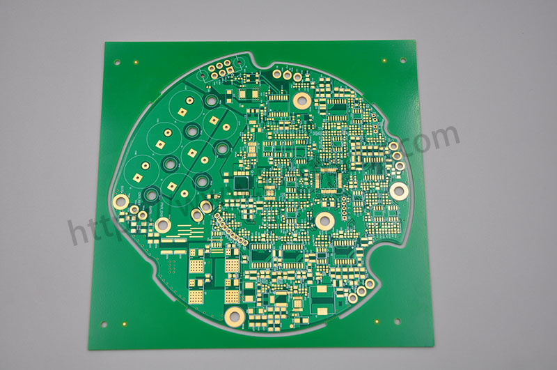
You may have found such a situation, most of the PCB boards are with green colors, while other colors are relatively rare to see, do you know why?
As we know that the Printed Circuits Board consists of Solder Mask Layer, Silk screen layer, solder PAD, Copper traces, surface finishing and other parts, etc.
Among them, the solder mask refers to the part of the PCB that is covered by oil. Since most PCB boards use green oil, the part of the green oil that can be seen on the board surface is the solder mask, which play an important role during the reflow soldering process.
green solder mask
Then why are most of the PCB boards green? The main reasons are as follows:
Green is less irritating to the eyes. We all know that green is good for the eyes and can resists fatigue. So when the PCB board with green solder mask, relative production and maintenance personnel are not prone to eye fatigue when staring at the PCB board for a long time, and it is less harmful to the eyes.
2. Cost for Green oil is lower. Since green is the mainstream in the production process, the purchase of natural green oil will be larger, and the purchase cost of green solder mask will be lower than other colors. At the same time, using the same color oil in mass production can also reduce the replacement cost.
When the board works on the SMT soldering process, it needs to go through the process from Tinning, post soldering and final AOI inspection. These processes all need to be optically positioned and calibrated. The green background color is better for the recognition of the instrument.
PCBA AOI testing
Okay, now, do you understand why most of PCB boards are with green colors?
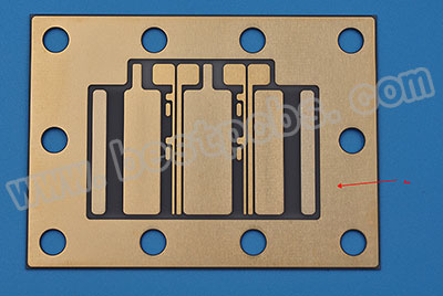
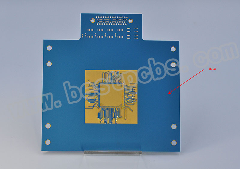
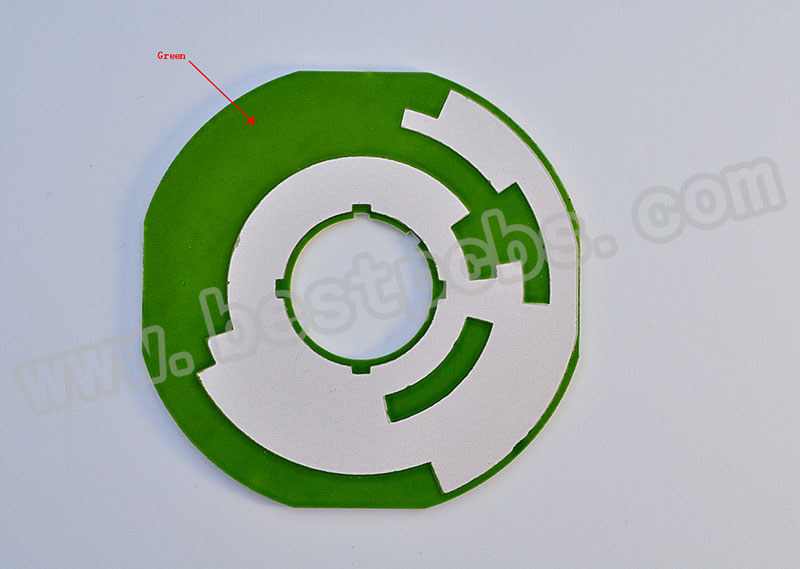
Though we know green is the most common one, but other colors such as red, yellow, blue, purple, black or some other colors are okay for us to make.
solder mask colors
If you have PCB board with a special color want to make, please contact us and we will try best effort to meet your request.
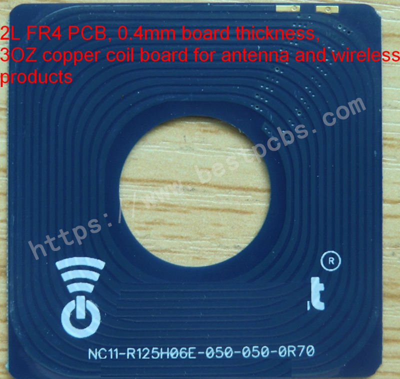
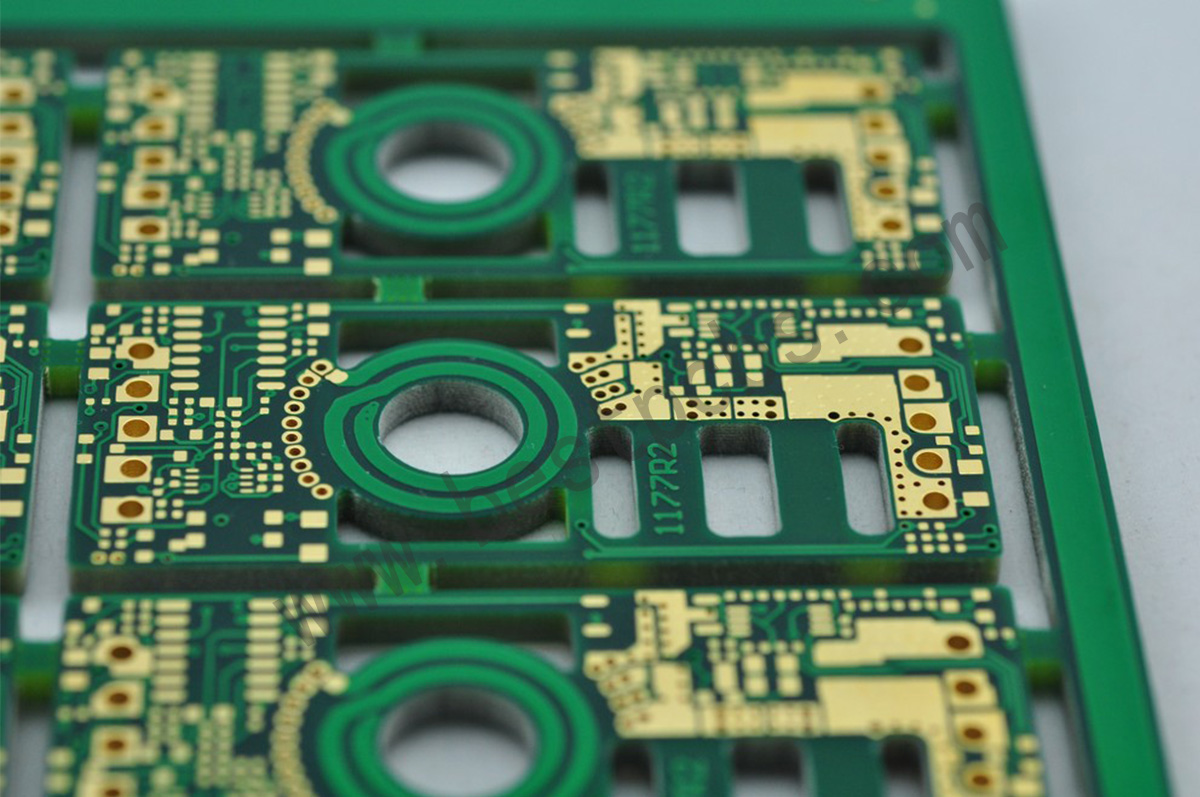
In year 2019, one of our US customers asked us, Marina can EBest Circuit (Best Technology) make a Coil PCB (Printed Circuit Board) with FR4 material? Yes, of course, we can make different kinds of PCB for our customer, included for the Coils PCB, which currently is widely used for wireless charging and antenna products. Please see the following Coils board from EBest Circuit (Best Technology).
The manufacturing process is same as other PCB manufacturing process, and just make sure the etching process and pay attention for the etching tolerance of the coils trace. And when coils PCB board finished, do you know what kind of test need to do to check the functional of Coils boards?
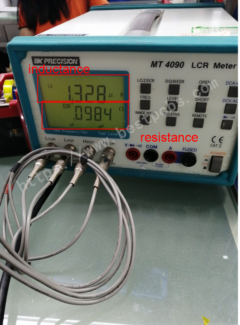
Today I would like to share how EBest Circuit (Best Technology) test Coil PCB board. Everyone knows that we check the quality of PCB board with Flying probe tester, as the production efficiency is extremely low and the inductance and capacitance cannot be accurately measured. In this way, we need to use LCR meter to make verify the inductance and capacitance. See the LCT meter as following.
EBest Circuit (Best Technology) chooses the digital meter LCR Meter to test the impedance characteristics of the coil. From the LCR tester you know see two numbers, one for inductance and another for resistance.
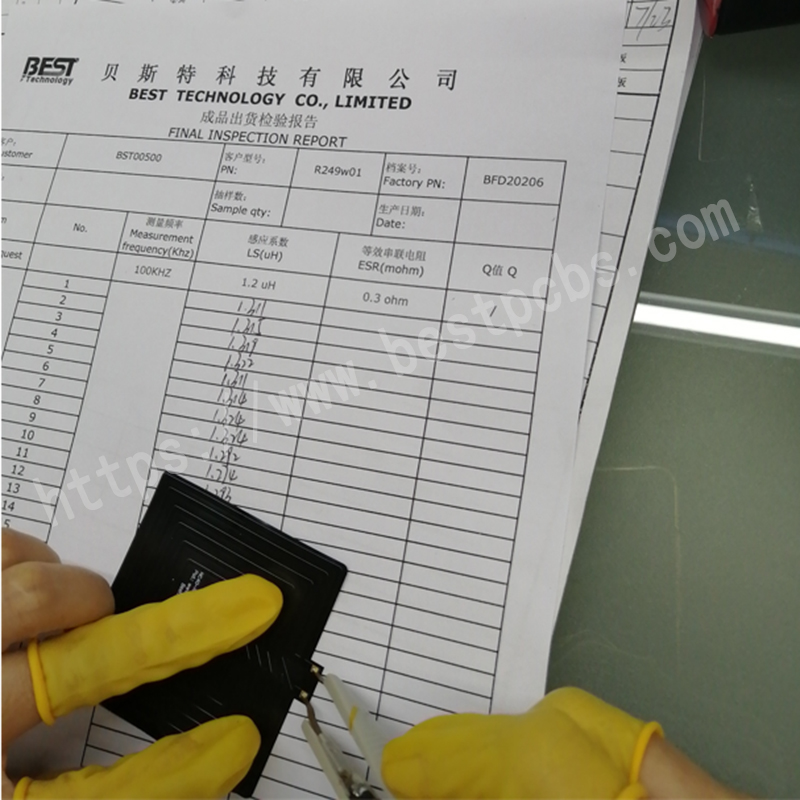
After test each coils printed circuit board, we will make record at our paper to make sure every measurement data will meet for customer requirement.
Currently, LCR Meter only provides a single-channel test function, and can only test the impedance characteristics of a set of coils at a time. But this is the effective test method for Coil printed Circuit Board. But we believe we will buy more LCR meters to let the test coil board become quicker.
If you have any comments on the testing for Coil printed circuit board, you are welcome to send us query and we are happy to discuss with you. You can visit www.bestpcbs.com to know more about us. Thank you
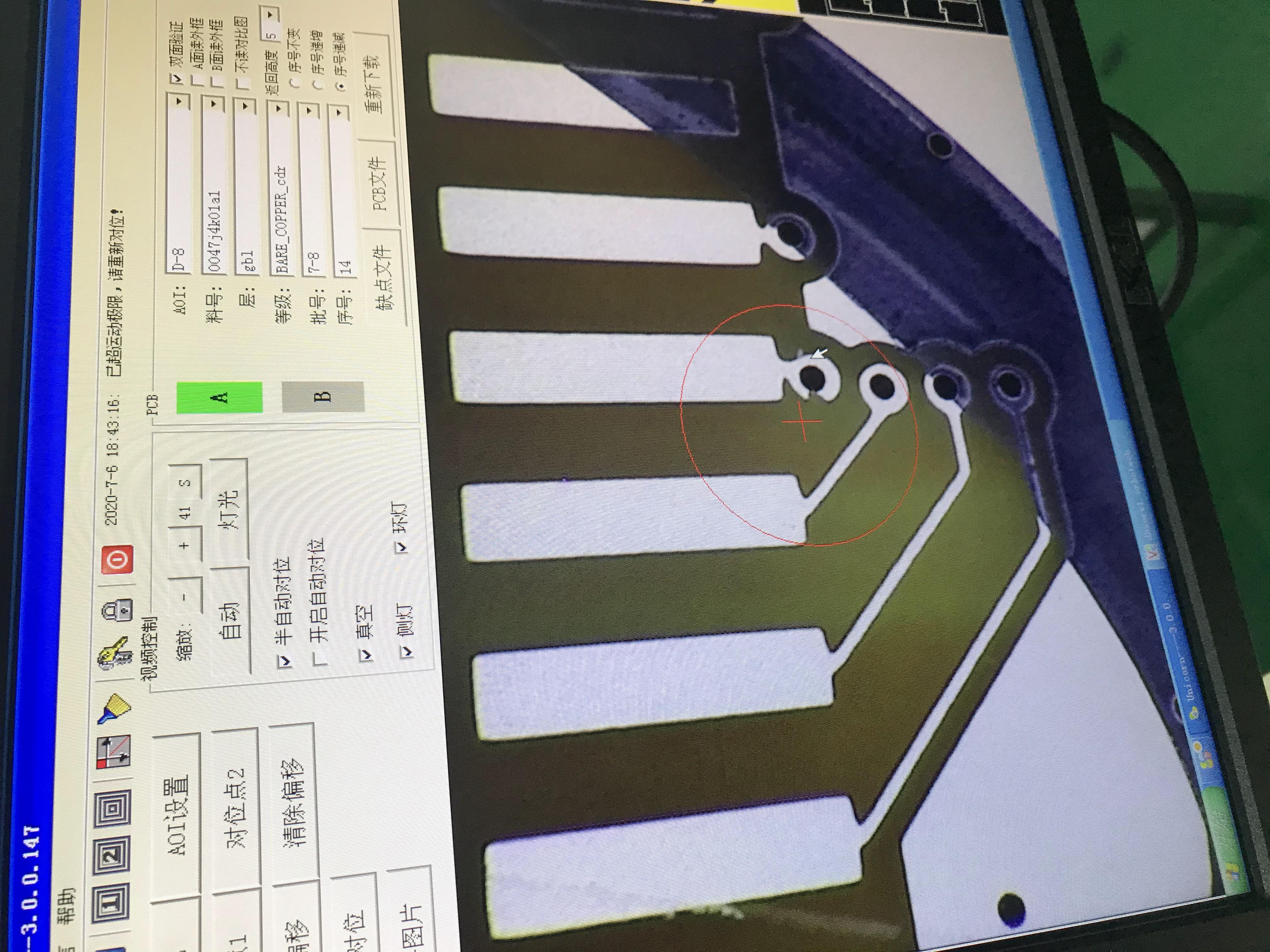
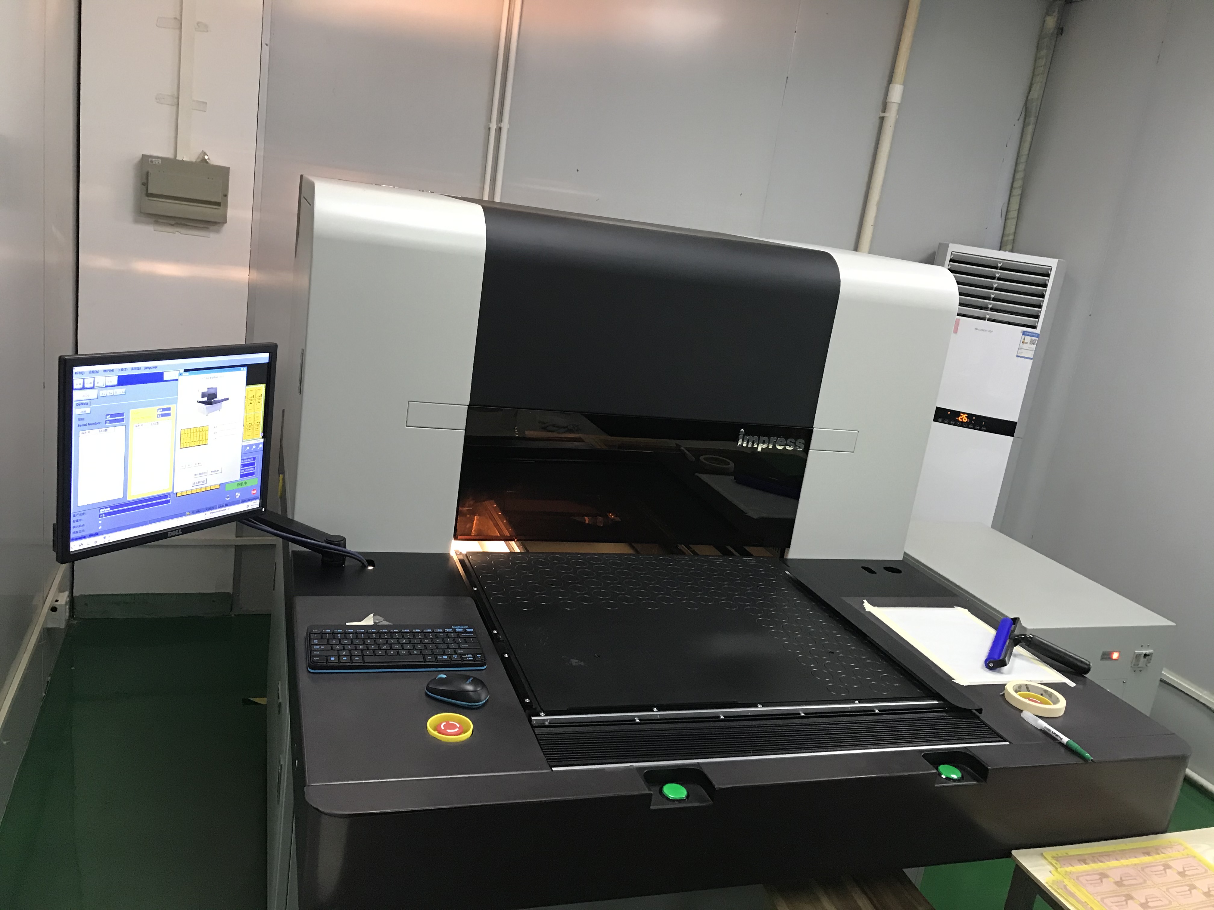
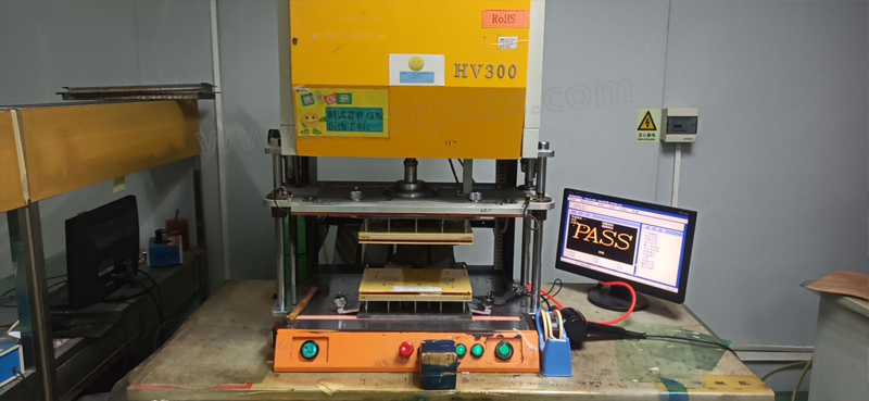
When the bare Printed Circuit Board qty become volume fabrication, the PCB manufacture will not use the Probe flying tester to test the PCB circuit board. Best Tech will make new PCB test fixture to test the bare PCB, The electrical Test (E-test), which is the final electrical test to verify net continuity and the absence of shorts on the bare printed circuit boards (PCBs). In Best Tech PCB factory, we perform 100% electrical testing on all bare PCBs its facilities as per IPC-6012 class 2 standard. And from the following photo in computer, you can see it will show PASS for PCB.
in test
in test
To test the PCB boards, we require the NETLIST file. Normally we create a reference netlist file from the customer’s original Gerber files during PCB fabrication.
We always prefer to receive the CAD file based on the netlist for comparison. Since a CAD based netlist is generated before PCB routing, it provides another layer of checking (against the Gerber files). This allows us to catch any PCB faults introducing in the event of an error in the Gerber files. For full turnkey PCB assembly (PCBA service) projects, this helps to ensure that the PCB boards are 100% correct before any components are populated.
tester 2
tester2
Here are Best Tech E-tester Capabilities
Minimum Continuity Resistance
0.1 Ohms
Maximum Test Voltage
1000 Volts
Max Isolated Resistance
25 M Ohm – 2 G Ohm
Electrical Test Pitch (Fixture)
20mil(0.5mm)
Electrical Test Pitch (Flying Probe)
4mil
Debug /check for missing pins: (Test fixture)
10 minutes
Test time per board:
40 seconds
Setup time:
30 minutes
All points are tested simultaneously. However, this process involves set-up to create the fixture itself and additional costs associated with the cost of materials.
The electrical test fixture has a limited shelf life and repeat using times. For every PCB it will need a fixture and its custom-made for a customer only. Many other factories only store 2 years shelf life for electrical test fixtures, but Best Tech will store at least 3 years for customer.
In order to ensure the quality of fixtures and spare enough space to store fixtures, Best Tech leaves one floor to keep the fixture. See attached fixture photo.
tester 1
tester1
During the 3 years’ time, customer no need to pay the fixture charge again if the update is no update. The flexible test fixture shelf-life policy, it will help customer save the cost.
At the end of the PCB production process, we use electrical test to check the interconnectivity of the PCB is correct against the original board data.
Best Tech did the E-Tester to test the PCB 100% before delivery to customer, this makes Best Tech get highly comments from our customer on the world with good printed circuit board quality and best service. See the customer highly comments of Best Tech.
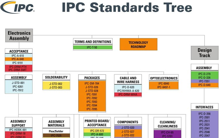
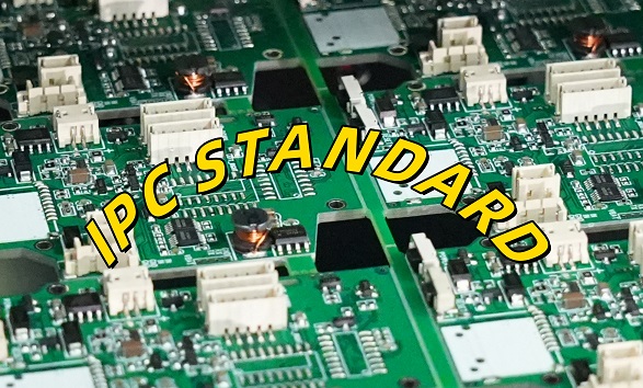
Do you know what is IPC standard for PCB?IPC, it is a trade association whose goal is to standardize the assembly and production requirements of electronic devices and components. It was established in 1957 as the Institute of Printed Circuits. IPC has developed thousands of standards and specifications to regulate the electronics manufacturing industry.
IPC standards are related to PCB design, production technology, electronic assembly, etc., in order to achieve high reliability, high quality, high performance, and meet user specifications.
What are the IPC Standards for?
Before we can understand IPC standards, we first need to know who made them. It comes from the IPC Association, a trade association whose goal is to standardize assembly and production requirements for electronic devices and components. It was founded in 1957 as the Printed Circuit Research Institute. Its name was later changed to the Institute for Electronic Circuit Interconnection and Packaging to highlight the expansion from bare boards to packages and electronic components. In 1999, the organization officially changed its name to IPC with the slogan “Association Connecting Electronics Industries”.
IPC standards are the most widely recognized code of acceptability in the electronics industry. The organization publishes standards for nearly every stage of the electronic product development cycle, including design, procurement, assembly, packaging, and more. In other words, IPC standards refer to everything in the electronics industry and are the basic knowledge of designers and manufacturers.
Just like the IPC standards tree, there are many different aspects of standards that all serve the end product. IPC-A-610, for example, focuses on the acceptability of electronic components and is used worldwide by original equipment manufacturers and EMS companies.
What is the PCB IPC Standard?
IPC plays a vital role in the PCB industry by establishing standards that cover every stage of PCB production from design to manufacturing. These standards ensure consistency and compatibility throughout the PCB process. During the design phase, IPC standards guide file formats, PCB design software, design guidelines, and electronic product documentation. They also affect the material selection of PCB components, surface mount equipment and surface treatments. In addition, these standards are essential for testing and evaluating the acceptability of printed boards.
When it comes to welding, IPC standards cover a variety of techniques, including reflow soldering, wave soldering and welding. These guidelines help companies determine whether their electrical and electronic components meet quality expectations during manufacturing. IPC standards also address cable and harness assemblies to ensure they meet standards.
The most widely recognized IPC standard for PCBs is IPC-6011, which Outlines the performance requirements for PCBS. However, IPC-6012 is more specific and governs the qualification and performance of rigid PCBs. IPC-6012 covers everything from how the PCB should be made to its thickness and the integrity of the copper layer. Compliance with this standard ensures that PCBs meet electrical and mechanical performance expectations. Whether you’re creating boards for high-end computers or small consumer devices, compliance with PCB IPC standards is critical to meeting industry and customer expectations. Here is the IPC tree for your reference:
What is the IPC Level of PCB?
One of the most widely used industry standards in the manufacturing of printed circuit boards is IPC-A-610C Acceptability of Electronic Assemblies and IPC-A-600 Acceptability of Printed Boards. This standard is used primarily for the incoming inspection of bare boards from a PCB fabricator.
In the IPC-A-610C document, electronic products are divided into level 1, level 2, and level 3. The higher the level, the stricter the quality inspection conditions. Here are how 3 levels divided:
Level 1 products: called general-purpose electronic products. Including consumer electronic products, certain computers and their peripherals, and products whose main purpose is to use functions.
Level 2 products: called dedicated service electronic products. Including communication equipment, complex industrial and commercial equipment and high-performance, long-life measuring instruments. Under normal use environment, this kind of product should not malfunction.
Level 3 products: called high-performance electronic products. Including high-reliability, long-life military and civilian equipment that can continue to operate. This kind of product must not allow any interruption failure during use, and at the same time, it is necessary to ensure the reliable startup and operation of the equipment in a harsh environment. Such as medical life-saving equipment and all military equipment systems.
For PCB manufacturing, do you know which IPC standards are commonly used?
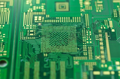
multilayer pcb
IPC Standard for PCBs
The IPC has created several standards for printed circuit board (PCB) design, manufacturing, and assembly. Here I would like to share you some standards which we mainly use:
IPC-2221
A general standard that covers almost every aspect of PCB design, including electrical considerations, thermal design, and manufacturing-ready design.
IPC-2222
A guide for rigid PCB cross-sectional design, including recommendations for board thickness, hole aspect ratio, and dielectric clearance.
IPC-2223
A standard for reliable Flex-PCB design, including guidelines for material selection, impedance control, and pad placement.
IPC-2224
A standard for PC card form PCBs, including design requirements for organic and inorganic materials, and single, double, or multilayered interconnections.
IPC-A-610
A standard for PCB assembly that classifies PCBs into three quality levels, with Class 1 being the lowest and Class 3 being the highest.
IPC-6011
General Performance Specification for Printed Boards
IPC-6012
Appraisal performance and specifications for Rigid printed boards
IPC-6013
Appraisal performance and specifications for Flexible printed boards
Appraisal and performance of permanent performance
IPC-HM-860
Multilayer Hybrid Circuit Specification
J-STD-003
Solderable test for printed boards
IPC-A-600F
Acceptance conditions for printed boards
IPC-4761
Design Guide for Protection of Printed Board Via Structure
resin filled production bpm20599
What is IPC-A-610 Standard?
IPC-A-610 Standard is one of the most widely recognized standards in the electronics industry, specifically focusing on the acceptability of electronic assemblies. It provides detailed guidelines and criteria for the inspection of PCB assemblies, so that these assemblies meet the necessary quality levels for their intended use. Its main content includes:
1. Soldering Criteria
IPC-A-610 provides in-depth guidelines on acceptable soldering techniques, covering solder joints, surface mount devices (SMDs), through-hole components, and wire terminations. It explains what constitutes an acceptable versus defective solder joint, ensuring that the electrical connections are reliable.
2. Component Placement
The standard includes criteria for the correct placement and alignment of electronic components on PCBs. It specifies the acceptable tolerances for misalignment and ensures components are correctly placed for proper electrical performance and physical integrity.
3. PCB Assembly Defects
IPC-A-610 details different types of assembly defects, such as insufficient solder, tombstoning, lifted pads, and more. Each defect is categorized based on its severity and impact on the function and reliability of the product, providing guidance on whether a defect can be accepted or if it requires rework.
4. Classes of Electronic Assemblies
The standard divides electronic assemblies into three classes based on the end-use of the product:
Class 1 – General electronic products
Class 2 – Dedicated service electronic products
Class 3 – High-performance products
5. Mechanical Assembly
IPC-A-610 provides criteria for the mechanical aspects of PCB assemblies, such as mounting hardware, screws, connectors, and wire routing.
6. Coating and Potting
The standard covers the application of protective coatings (conformal coatings) and potting materials that protect the PCB from environmental damage such as moisture, dust, or chemicals. It specifies acceptable thicknesses, coverage areas, and inspection methods.
7. Cleaning Requirements
The cleanliness of PCB assemblies is critical for preventing performance degradation over time. IPC-A-610 outlines acceptable levels of residues from fluxes and other contaminants and specifies methods for inspecting and verifying cleanliness.
8. Cable and Wire Harness Assemblies
The standard includes requirements for assembling and inspecting cable and wire harnesses.
9. Solderless Wire Wraps
The standard also touches on solderless wire-wrapped connections, which are used in some applications where soldering is not practical or preferred. IPC-A-610 defines the acceptable criteria for such connections.
10. Inspection and Testing
The IPC-A-610 standard provides guidelines for visual inspection and testing methods used to evaluate whether an assembly meets the required acceptability criteria. This can include both automated and manual inspection processes, depending on the class of product.
Why IPC Standard is Important?
IPC standards are of great importance to the circuit board industry.
1. IPC standard specifies the requirements for all aspects of the design, manufacturing and assembly of the circuit board, including material selection, size specifications, welding quality, reliability testing, etc., providing a unified reference and guide for circuit board manufacturers to improve product quality and reliability.
2. IPC standards can help communicate and cooperate between PCB manufacturers and customers. By referring to IPC standards, the two parties can reach a consensus on PCB specifications, quality requirements and other aspects, reduce misunderstandings and disputes, and improve production efficiency.
3. For customers, IPC standards provide confidence. When a company adheres to these standards, they can trust that the final product will be reliable and durable, even in demanding environments.
4. In addition, IPC standards also contribute to the technological innovation and development of the circuit board manufacturing industry. By being in line with international standards and understanding the latest technological trends and standard requirements, manufacturers can continuously improve production processes and equipment, improve production efficiency and product quality, and enhance competitiveness.
At the same time, IPC regularly updates and revises standards to meet changing technology and market needs.
What is the IPC Standard for PCB Clearance?
PCB clearance, or the distance between conductive components, is essential to avoid electrical shorts or interference. Without proper clearance, electrical shorts could occur, potentially leading to device failure or safety hazards. The IPC-2221 standard covers PCB design and provides guidelines for this clearance, ensuring safety and functionality. This standard specifies how much space is needed between traces, pads, and other conductive materials depending on the operating voltage. However, the minimum clearance between any two conductors on a PCB depends on the device’s intended use and voltage:
General-purpose devices: 0.1 mm (4 mils)
Power conversion devices: 0.13 mm (5.1 mils)
Class 2 and 3 PCBs: 0.25 mm (10 mils) for low voltage and 0.5 mm (20 mils) for high voltage
What are the IPC Standards for PCB Repair?
PCB repair can be tricky, but IPC-7711/7721 offers guidance on how to properly rework and repair PCBs. These standards provide detailed procedures for everything from removing defective components to repairing damaged traces and soldering issues.
By following IPC-7711/7721, technicians can restore a PCB to its original condition without compromising its performance. This is critical in industries where PCBs are expensive or difficult to replace, such as aerospace and medical devices. Repair standards also reduce the environmental impact by extending the life of the PCB, making repairs more sustainable.
It is no problem for us to manufacture the PCB following the standard in IPC 6012 /6013 Class 2 and Class 3, as well as following to the standard listed above. These acceptance conditions are the basis for the inspection of our company’s products, as well as the working standards of the employees at the production site, and also become an important part of the training of the employees for PCB production and assembly in our company.
Send us your PCB drawing, let’s help to make your PCB design into a real board.
Before leaving PCB manufacturing line, bare PCBs (Printed Circuit Boards) have to pass electrical tests so that it guarantee that boards go for high performance and high reliability after finish the SMT(Surface Mount Technology). Electrical tests are implemented to find out electrical and circuitry issues such as shorts, opens, resistance, capacitance etc. all of which indicate whether bare boards or assembled board are correctly fabricated.
shorts circuit
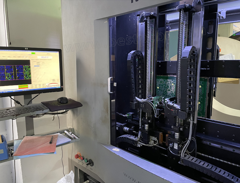
When test probes work, it moves quickly from test points to other test points as per instructions instructed by the computer set up program. Â
probe flying test
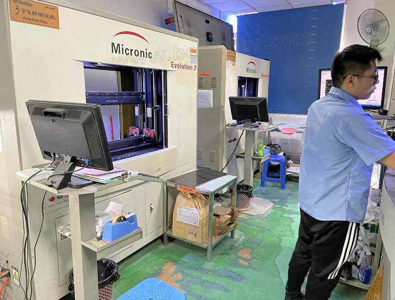
Probe test is no need fixture, so it is very popular in the printed circuit boards manufacturing. The most significant reason is their cost. it is highly cost-effective for prototypes and low to mid-volume production. And the most important factor, the test reports can be provided for each board after finish tested and it is very easy to export from the computer, you can send to your customer very quickly for the test results of PCB.
Advantages of Flying Probe Test:
Low test cost (Eliminates fixturing costs and time)
Short test development time
Fast computer program development, easy integration of design changes
Rapid feedback provided to PCB design engineers at prototyping period
Process flexibility
Circuit access, even in the absence of test points
Controlled probe contact, programmable for any type of board
Different test solutions and approaches integrated in a single test system
Intrinsic positioning and measurement precision
Disadvantages of Flying Probe Test
Everything has two sides. Apart from obvious advantages, flying probe test have some disadvantages.
Since flying probes have direct physical contact with vias and test pads and small pits are easily caused on board surface, when flying probe tester is working on components without test pad, it’s possible that probes have contact with component leads so that loose leads or leads with badly-performed soldering may be missed.
In spite of the disadvantages mentioned, flying probe test is still regarded as a significant test method for PCB fabrication. Flying Probes have enhanced the competitive variable as lost time due to retooling has been removed. Prototype and Quick Turn product is the perfect match for Flying Probes as they carry out in low quantity orders and are quick to change jobs, unlike the long setup times with fixture testers.
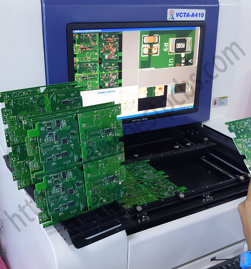
By the way, to test circuit shorts, opens, EBest Circuit (Best Technology) also do AOI checking to make sure there is no issue for PCB manufacturing.
AOI test
Contact EBest Circuit (Best Technology) right now, to discuss more for printed circuit boards.
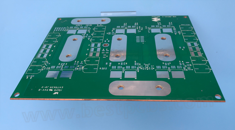
In EBest Circuit (Best Technology), currently the most common metal used for Metal Core PCB manufacturer are Aluminum, Copper. Today let’s talk about the main differences between aluminum substrate and copper substrate, hoping to help you choose the right substrate in future design projects.
Although they both share similar properties and functions, there are still a few variations between the two kinds of metals. Some of the key differences between aluminium and copper core PCBs are explained in the points below.
1. Thermal Conductivity
The thermal conductivity of copper substrate is up to about 400(W/mK) and the thermal conductivity of aluminum substrate is generally about 200W(W/mK). The thermal conductivity is higher, the transfer efficiency will be better, and the heat dissipation will be better, then the working life will be longer.
 Thermal Conductivity
2.Electrical Conductivity
Both aluminum and copper, being metals, are electrical conductors of electricity, although the exact degree of this varies between the two metals. When it comes to electrical conductivity, copper has a clear advantage over aluminum. In other words, in applications where there is a need for efficient electrical conductivity, copper makes for an ideal pick.
 Electrical Conductivity
3. Electrical Resistance
Resistance is very important when it comes to PCB design, as it can have an effect on the overall function and stability of the component. Given that copper has a higher density than aluminum, it tends to have a lower resistance than aluminum, so copper is an better choice where there’s a requirement for thinner circuits and faster electricity transfer.
Electrical Resistance
4. Weight
Since copper has the higher density for per unit area, the weight of copper PCB is much heavier than aluminum PCB for the same design.
In applications where light-weight construction is required more than anything else, aluminum is the preferred material of choice. On the other hand, applications where weight is not much of an issue, tends to be the ones where copper is widely used.
Weight
5. Application
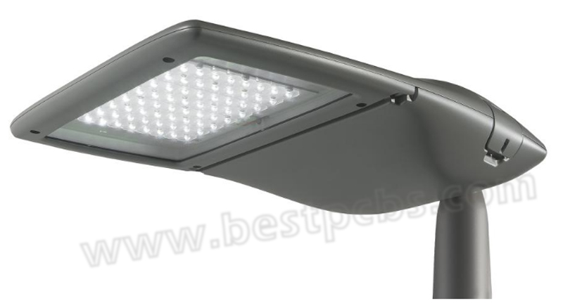
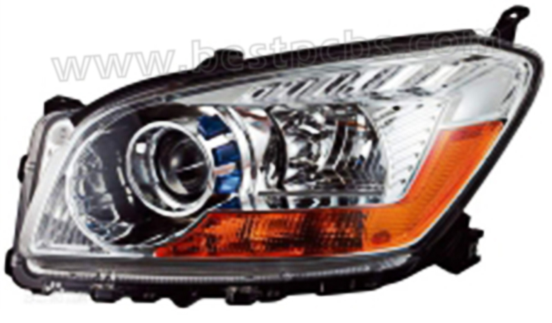
Copper core PCB is the best heat dissipation among all MCPCB, so it’s mostly used in automobile headlights, taillights and some high-tech electronic products (unmanned aircraft, mining machine) high-power lighting equipment. The aluminum core PCB is mostly used in indoor lighting, energy saving lighting, street lighting and other energy-saving lighting electronic products.
Application
Application
In conclusion, due to the above different parameters and performance, the cost of copper is generally more expensive than aluminum. If you have other questions about MCPCB, welcome to contact us .
Every printed circuit board need to do full test before ship to our customer. but you may have doubt, the PCB was made according to the original Gerber file, why finish the PCB production process, why the short Circuit will occur on a FR4 circuit board?
A short circuit may also occur during reflow soldering. the solder paste may accidentally connect two pins that are very close to each other. In some cases, errors can occur during the PCB design process because the wiring between different networks accidentally connects.
We believe every PCB manufacture have their own test method to do short circuit, but today I would like share how EBest Circuit (Best Technology) to Check for Short Circuits in a Printed circuit board.
Here are some important steps:
Step 1 Visual inspection
The first step for locating short circuits on PCB is to carefully look at the entire surface of the PCB. EBest Circuit (Best Technology) QC guys use a magnifying glass or low magnification microscope during the circuit board examination. We check the whole board surface to see if there are some traces break off. Any cracks or blobs of solder should get careful attention. Check all your vias. If you specified unplated vias, make sure that’s the case on the board. Poorly plated vias can create a short circuit between layers and leave you with everything tied to ground, VCC, or both.
visual inspection
All the testing work will carry out according to IPC 6012 class 2.
Step 2 Use a Digital Multimeter to find out where is the problem
To test a circuit board for a short circuit, you need to check the resistance between different points in the circuit. If visual inspection doesn’t reveal any clues as to the location or cause of the short circuit, grab a multimeter and try to track down the physical location on the printed circuit board. The multimeter approach gets mixed reviews in most electronics forums, but tracing your test points can help you figure out what isn’t the problem.
Step 3 use Probe flying Tester &E-tester
As long as you are in Printed Circuit board field, you are definitely known Probe flying test and E-Teter.
Flying probe test systems require no test fixture, it can serve both prototype and small production, providing maximum flexibility for PCB manufacturers and this job can complete in a short time.
probe flying test
probe flying test-1
But when your circuit board become to volume, you will need to open a test tooling/test fixture to test the Printed Circuit board to test the open short circuit.
E-tester
In my next blog in June, I will introduce Probe flying test to you in more detail.
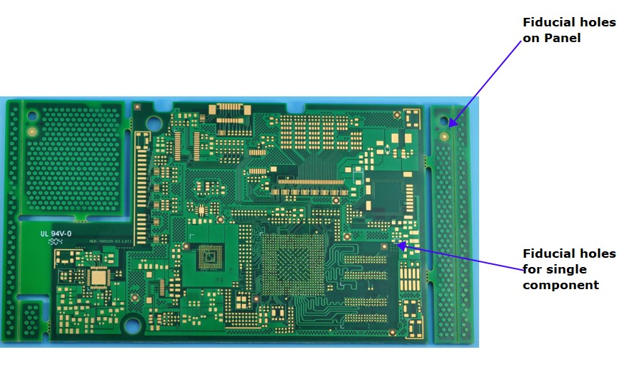
You may ever be recommended by some PCB manufacturers to add the fiducial holes on the board edge. Do you know what is fiducial marks and what’s the purpose for this kind of holes in a PCB?
Now, let me to show you something for what is the fiducial holes.
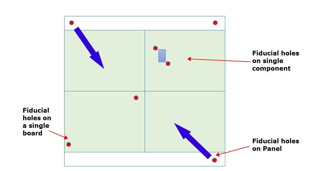
Fiducial holes, we also call it fiducials mark, while we assemble a PCB, it will need to locate the positions for each component, and it is positioned based on the fiducial mark as the reference point.
There are 3 types fiducial marks, first type is fiducial marks on a single board, second type is the fiducial marks on a PCB panel, third one is the fiducial marks for some single component on the board.
Here are the pictures for you to understand the types of the fiducials.
Fiducial holes types
Fiducial holes
Fiducial mark on a single board is designed for positioned all circuits features on a single board. It is necessary to have a fiducial mark on a single board.
And fiducial marks on a PCB panel is used to assist positioning the circuits.
For the fiducial mark of a single component, it is designed to position the fiducial mark of a single component, which can improve the placement progress (For QFP, CSP, BGA and other important components must have the fiducial marks).
So, it is important to add the fiducial holes on a PCB board.
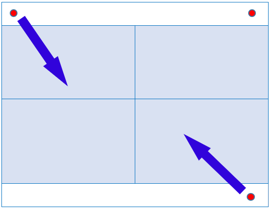
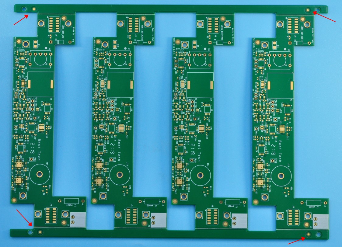
Also, while we make the panel for the PCB board, on the diagonal of the four corners, it is required to have 2 fiducial points at least on 2 diagonal corners. you can also place 4 marks on the four corners, but generally, assembly plant will only need 2 marks for recognize.
See below a PCB panel for reference:
PCB panel drawing EBest Circuit (Best Technology)
Fiducial holes on a panel
In the other hand, while you design the PCB, please try not to put the silk screens, pads, traces etc. within 2mm of the optical fiducial marks. Otherwise, the SMT machine will not be able to recognize the optical fiducial on the PCB boards.
And if you add the fiducial holes on the area which without any circuits, to avoid the holes being etching while the process, so generally we suggest to add a metal circles around the fiducial holes, to make it more obviously on the boards.
If you have any new PCB design which you also want to add the fiducial marks.
You are welcome to contact EBest Circuit (Best Technology) for a help and we will show our best help for you.
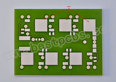
Ceramic PCB including Alumina PCB (Al2O3 PCB), Aluminum Nitride PCB (AlN), Bryllium Oxide PCB(BeO PCB) etc.
There are other differences except the substrate material is different.
The method of making conductor is different.
The conductor for thick film ceramic is made by printing, but DPC is made by vacuum sputtering and plating.
The conductor is different.
The conductor for thick film ceramic PCB is Au or AgPd, but for DPC ceramic PCB, it is copper.
The thickness of conductor is different.
Normally, it is 10-20um for thick film ceramic PCB, copper thickness can be 10um-300um for DPC ceramic PCB.
The solder mask is different.
It is glass glaze for thick film ceramic PCB, the most popular color is greenish and blue. Glass glaze can withstand very high temperature, up to 850C
It is normal solder mask oil for DPC ceramic PCB, the most popular color is white.
The above is only simple introduction for the difference, if you want to know more differences between thick film ceramic PCB and DPC ceramic PCB or other details about ceramic PCB, please contact us
In the Printed Circuit Board industry, believe that you are familiar with blind via and buried via. What is blind via and buried via for PCB? And do you know is the Blind via or Buried Via have special application in your Printed Circuit Board?
In order to know more, we would like to share more information with you today.
EBest Circuit (Best Technology)Â is an experienced FR4 PCB manufacturer in China since year 2006, with more than 15 years design and fabricate experience for PCB, EBest Circuit (Best Technology)Â accumulated more than 1000 customers from all over the world.
Before start, we need to know what kinds of hole for FR4 Circuit Board, Via, Blind Via and Buried Via.
What is a Via?
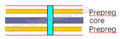
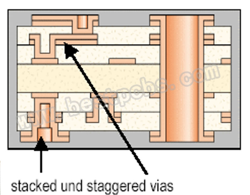
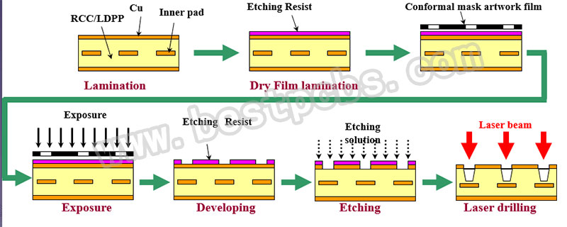
Vias are the copper-plated holes in the PCB that allows the layers to layer connection. The standard via is called a through-hole via, but there are several disadvantages to using through-hole vias in Surface Mount Technology (SMT). For this reason, we often use a blind via or buried via instead. A blind or buried via can be processed in a wide range of different measures, including plugged copper mask via, a plugged solder mask via, plated via or staggered via.
Via
staggered via
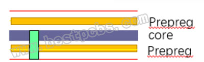
What is Blind Via?
The via connects the external layer to one or more inner layers of the PCB and is responsible for the interconnection between that top layer and the inner layers.
Blind Via
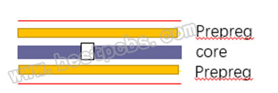
What is Buried Via?
For a buried via, is the inner HOLE, between both sides in the board up and down inside the layer after pressing is cannot see. So, it doesn’t have to take up the outer area.
Buried Via
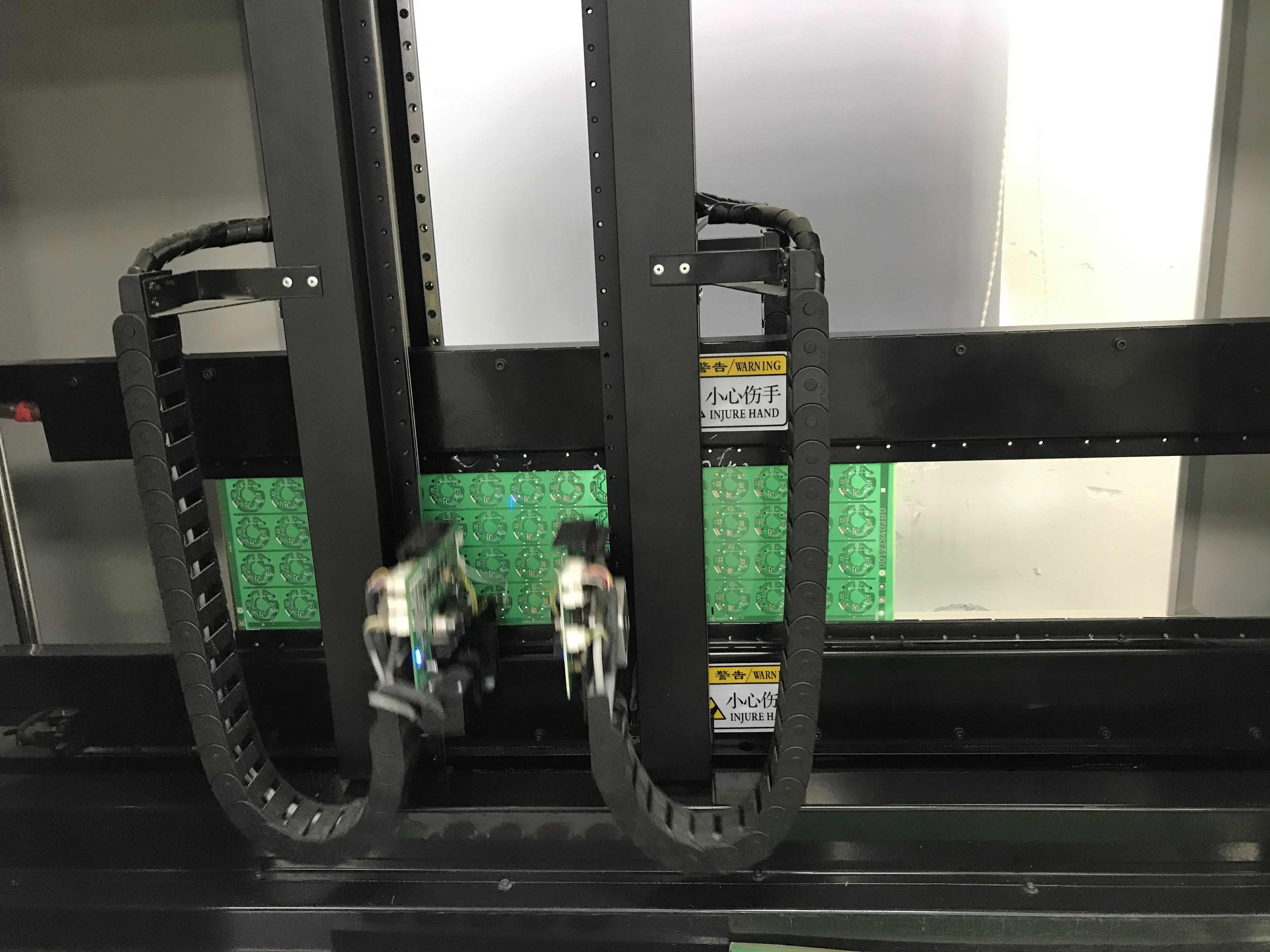
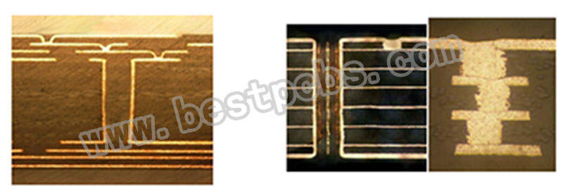
Blind and buried vias are particularly advantageous in HDI board because they optimize the density of the boards without increasing board size or the number of board layers you require. They are most commonly used in high-density PCB designs like, or in FPGA and custom chip packaging.Here is the photo which EBest Circuit (Best Technology) took from our production line to make HDI Printed Circuit Board for our USA customer.
HDI board under production
HDI process
EBest Circuit (Best Technology) is a very professional manufacturer in printed circuit board and HDI Board. If you are interesting to know more information of us, come to contact us and we are looking forward to discuss with you more for Printed Circuit Board.