Why choose MIS substrate? Let’s discover features, applications, difference between traditional PCB, design consideration, production process for MIS substrate.
Are you troubled with these questions?
- Difficulty in 3D structure molding?
- High heat loss in high-frequency scenarios?
- High mass production costs and low yield?
As a MIS substrate supplier, EBest Circuit (Best Technology) can provide you service and solutions:
- Collaborative Design: Simulation verification helps avoid pitfalls in advance, significantly reducing trial-and-error costs!
- Flexible Customization: <50μm fine circuitry + embedded components, meeting all your needs!
- Reliability Guarantee: Stable operation from -40℃ to 125℃, 10+ year lifespan, worry-free after-sales service!
Welcome to contact us if you have any inquiry for MIS substrate: sales@bestpcbs.com.
What Is MIS Substrate?
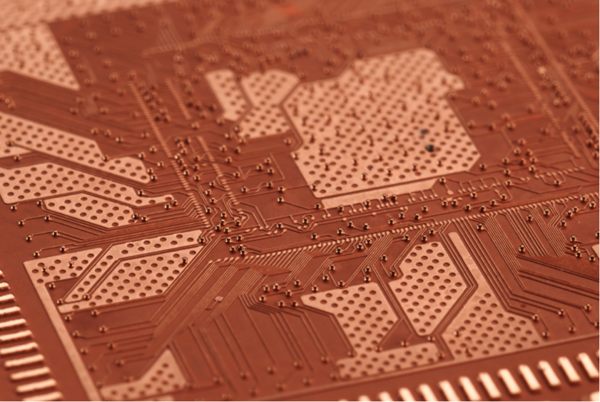
MIS Substrate, also called as Molded Interconnect Substrate ( is an advanced packaging substrate technology. It uses injection molding to directly embed conductive lines (usually copper) into the interior or surface of an insulating resin material (usually epoxy resin), forming a three-dimensional substrate with intricate circuit patterns. Unlike traditional etching methods (etching away excess copper foil on a copper-clad laminate to form circuitry), the core of MIS is molding and Laser Direct Structuring (LDS) or similar patterning techniques.
What Are Features of MIS Substrates?
Features of Molded Interconnect Substrate:
- 3D Design Flexibility – Supports curved/irregular shapes via injection molding, essential for compact/wearable devices.
- High-Density Wiring – Enables sub-50μm line precision for compact, high-speed packaging (e.g., 5G/radar).
- Embedded Components – Integrates passives directly into plastic, reducing external parts and size.
- Thin & Lightweight – Eliminates multi-layer PCB bulk, ideal for miniaturized electronics.
- Electrical/Thermal Performance – Low-loss plastics (e.g., LCP) suit high-frequency use; better heat dissipation than air.
- Cost Efficiency – Simplified process cuts costs for 3D/small-batch production vs. traditional substrates.
- Durability – Molded plastic offers vibration/stress resistance, enhancing reliability in harsh environments.
What Are Applications of MIS Substrate?
Applications of Molded Interconnect Substrate:
- High-Frequency/RF Applications: 5G/6G communication modules (antennas, RF front-end modules); millimeter-wave radar (automotive/industrial radar).
- Automotive Electronics: Radar, LiDAR cameras, position/pressure sensors; Advanced Driver Assistance Systems (ADAS) components.
- Consumer Electronics & Wearables: Smartphones/tablets; smartwatches/TWS earbuds/AR/VR devices.
- Medical Electronics: Implantable/wearable medical devices.
Difference Between MIS Substrate and Traditional PCB
| Feature | Molded Interconnect Substrate | Traditional Printed Circuit Board |
| Essence | 3D injection-molded structural circuit carrier | 2D planar laminated circuit carrier |
| Core Process | Injection molding + Laser Direct Structuring (LDS) / selective metallization | Copper-clad etching + laminate stacking (multilayer) |
| Structure | 3D stereoscopic structure (curved surfaces, irregular shapes, cavities) | Planar or multi-layer flat structures |
| Integration Density | Extremely high (embedded components, irregular surface mount) | Moderate (surface mount dominant, limited embedding capability) |
| Design Freedom | Extremely high (breaks planar limitations) | Limited (confined to planar stacking) |
| Typical Materials | Engineering plastics (LCP, PPS, PBT, epoxy + additives) | Fiberglass epoxy (FR4), polyimide, BT resin, etc. |
| Line Width/Spacing | Finer (up to <50μm) | Relatively coarser (mainstream >75μm, HDI down to 50μm) |
| Key Advantages | 3D form factor, high density, miniaturization, lightweight, high-frequency potential | High maturity, low cost (high volume), well-established design tools |
| Key Challenges | Material cost, process control difficulty, warpage management, design complexity | Difficult 3D structures, higher high-frequency loss (FR4), layer limitations |
Molded Interconnect Substrate Design Considerations
1. Material Selection and Performance Matching
- Metal Substrate Applications: Aluminum substrates (thermal conductivity 1.0–3.0 W/(m·K)) are suitable for high-heat scenarios like LED lighting. Copper substrates (0.5–1.0mm thickness) are used in high-frequency/EMI shielding applications. Balance thermal conductivity, cost, and processing difficulty. For example, aluminum offers lower cost but requires oxidation risk control, while copper provides superior thermal performance but demands EMI compatibility measures.
- Specialty Material Options: Silicon carbide suits automotive/aerospace high-temperature environments (>300°C) but incurs higher costs. PTFE (dielectric constant 2.1) or fluorinated polyurethane (dielectric constant 1.8) is used for high-frequency signal transmission, though mechanical strength requires composite design.
- FR-4 Optimization: Standard choice for general applications. Note dielectric constant drift (4.5–5.5) may affect signal integrity. For high-frequency scenarios, replace with Rogers ceramic substrates or hybrid material designs.
2. Thermal Management Strategies
- Copper Layer and Via Design: Use ≥2oz copper thickness in high-power areas, paired with arrayed thermal vias (diameter 0.3–0.5mm, spacing ≤1mm). Fill vias with copper or thermal adhesive to enhance heat conduction. Example: ≥8 vias beneath BGA packages to form thermal channels.
- Layout Optimization: Position power devices (e.g., MOSFETs) near PCB edges or heat sink mounting surfaces, reserving ≥5mm component-free zones. Maintain ≥2.5mm spacing (forced air) or ≥4mm spacing (natural convection) between heat-sensitive components (e.g., electrolytic capacitors) and heat sources. Distribute multiple heat sources to avoid localized overheating.
- External Cooling Enhancement: Integrate heat sinks (thermal pads/adhesives), forced air channels, or liquid cooling systems. Validate thermal performance via simulation (ANSYS) and post-layout testing (thermal imagers/thermocouples).
3. Structural and Electrical Design
- Metal Substrate Construction: Single-sided boards require dielectric layer bonding (hole diameter ≥1mm demands ≥0.5mm wall spacing). Double-sided/multilayer boards control total thickness (0.8–3.5mm, extreme 8mm). Rigid-flex designs balance rigid sections (e.g., cold plates) and flex zones, with drilling rules adhering to 10:1 aspect ratios (non-metallic holes).
- Signal Integrity: High-speed traces (e.g., USB3.0) maintain length tolerance ≤±5mil, differential pair length mismatch <2mil. Avoid critical signal traces crossing split planes; maintain reference plane continuity across via arrays. Orthogonal routing between adjacent signal layers enhances crosstalk control. Power/ground plane spacing ≤10mil strengthens plane capacitance.
- Power and Ground Design: 4-layer boards adopt “signal-ground-power-signal” stackup. 6-layer boards prioritize “signal-ground-signal-power-ground-signal” layouts. High-current paths (>1A) require ≥15mil trace widths, via inner diameters ≥0.5mm with thermal relief connections, and minimized loop areas.
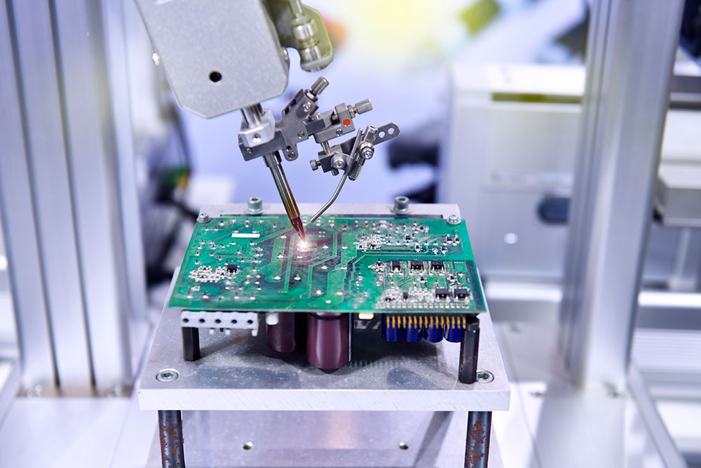
4. Manufacturing Process and Reliability
- SMT Assembly Control: Pre-bake metal substrates (125°C/2h) to reduce moisture. Reflow peak temperatures (235–245°C) are 5–10°C lower than FR-4. Nitrogen environments (<1000ppm O?) reduce oxidation. Solder paste stencil openings use “grid” segmentation to minimize voids. Pad extensions (0.05–0.10mm) compensate for CTE mismatches.
- Mechanical Strength and Tolerance: Metal substrate dimensional tolerance ±0.1mm (extreme ±0.05mm), V-cut depth ≤1/3 metal layer thickness. Panelization requires 3mm rails and dual tooling holes. Fixturing (vacuum suction/roller clamps) controls warpage ≤0.5%.
- Testing Validation: Thermal cycling (-40°C?125°C/500 cycles) ensures resistance drift ≤10%. High-voltage testing (1500V AC/60s) verifies leakage current ≤1mA. X-ray inspection confirms power device solder joint voids ≤20%.
5. Cost and Manufacturability Balance
- Hybrid Material Design: Localized high-heat areas use high-thermal materials (e.g., ceramic substrates), while FR-4 regions reduce costs. Metal-to-FR-4 bonding requires compatible dielectric layers (e.g., 2116/3313/1080) and avoids no-flow/low-flow materials.
- Process Parameter Optimization: Copper block thickness (1.0–3.0mm) and positions must be clearly specified. Connection areas require copper windowing and 0.3mm vent holes. Surface finishes prioritize ENIG/ENIP/hard gold over HASL for copper substrates.
- Failure Prevention: Measures include plasma cleaning, zoned temperature control, strict humidity/pressure management, and process optimization to maintain defect rates <50ppm. Mitigate risks like dielectric delamination (rapid preheat/peak temperature), copper foil blistering (moisture content >0.15%), and pad lifting (post-thermal shock bond strength).

MIS Substrate Manufacturing Process
1. Material Property Adaptation & Pretreatment
- Selection of engineering plastics (e.g., LCP, PPS, PEEK) or specialty resins to meet 3D molding, high thermal conductivity (≥3W/mK), and low CTE (≤20ppm/℃) requirements.
- Pretreatment includes drying at 80-120℃ for 2-4 hours to remove moisture, compounding with laser-activating agents (e.g., copper-chromium complexes), and DSC thermal analysis to verify material stability, ensuring no degradation during injection molding and uniform metal ion release during laser activation.
2. Precision Injection Molding Parameter Control
- Realization of 3D structures (curves, cavities, irregular holes) via servo injection machines and high-precision molds (tolerance ≤0.02mm).
- Parameters: injection temperature 250-310℃, mold temperature 100-120℃, cooling time 5-15s. Key controls include slope angles ≥30° to prevent demolding damage, via taper angles ≥60° to reduce plating defects, and surface roughness Rz5-10μm to enhance laser activation uniformity. Moldflow simulation optimizes runner design to avoid weld lines affecting structural strength.
3. Laser Direct Structuring (LDS) Technology Optimization
- Precise activation of conductive patterns using nanosecond pulsed lasers (355/1064nm) with dynamically adjusted energy density (5-12J/cm?), scan speed (2-4m/s), and frequency (40-100kHz).
- Pattern design avoids mold parting lines to prevent plating overflow, maintains line spacing ≥0.5mm to avoid short circuits, and uses 3D optical profilometry to verify activation depth (2-8μm) and surface uniformity.
4. Chemical Plating & Electroplating Enhancement
- Formation of 6-12μm uniform conductive copper layers via chemical plating (plating rate 0.5-1μm/h), followed by electroplating nickel (2-4μm for diffusion barrier) and gold (0.1-0.2μm for oxidation resistance) using pulse plating to minimize edge effects.
- SEM analysis of plating grain structure, ASTM D3359 cross-cut test for 5B-grade adhesion, 24h salt spray test for corrosion resistance, and plating thickness deviation ≤±10%.
5. Embedded Component Integration & Pre-Encapsulation
- Dispensing of conductive/non-conductive adhesives (e.g., silver paste, epoxy), component placement, and low-temperature curing (150-180℃ for 1-2h) followed by encapsulation with epoxy molding compound (EMC) or polyimide (PI) film for electrical connection and mechanical protection.
- Thermal management control (30% reduction in thermal resistance), support for multi-chip SiP integration, and X-ray inspection for internal void ratio ≤5%.
6. Design Verification & Manufacturing Feasibility Simulation
- Pre-manufacturing validation via 3D modeling and simulation: ANSYS for thermal-mechanical stress analysis, Altium Designer for PCB layout optimization to avoid high-frequency crosstalk, and Moldex3D for injection molding simulation to predict weld lines and filling defects, enabling design parameter optimization.
7. Full-Process Testing & Reliability Validation
- AOI for surface defect detection (e.g., line gaps, plating overflow), X-ray for internal void and solder joint analysis, thermal imaging for heat distribution uniformity (temperature difference ≤10℃).
- Electrical testing includes impedance control (50Ω±10%), signal integrity (eye diagram opening ≥70%), and HAST (130℃/85%RH/96h) for long-term reliability. Compliance with IPC-A-610 standards ensures stable operation from -40℃ to 125℃ with a lifespan ≥10 years.
Why Choose EBest Circuit (Best Technology) as MIS Substrate Supplier?
Reasons why choose us as MIS substrate supplier:
- Customized Design Expert Team: Equipped with senior PCB designers and material engineers, providing full-cycle design support from material selection to thermal management layout. Ensures solutions match specific application scenarios (e.g., high-frequency high-speed, high-temperature high-humidity environments), reducing design iteration time and costs.
- Stringent Material Quality Control System: Adopts ISO 9001-certified supply chain management. Conducts full-batch physical performance and chemical compatibility testing on materials such as aluminum/copper substrates, specialty ceramics, and PTFE. Ensures key parameters like dielectric constant and thermal conductivity deviations ≤3%, reducing risks of signal distortion and thermal failure.
- Advanced Manufacturing Process Guarantee: Features German precision drilling machines, Japanese optical inspection equipment, and vacuum laminating production lines. Achieves 0.1mm-level trace width/spacing control, 10:1 aspect ratio high-precision drilling, and multi-layer board layer-to-layer alignment accuracy ≤50μm, meeting complex design requirements.
- Full-Chain Reliability Verification: Provides comprehensive testing from thermal cycling (-40°C~125°C/500 cycles) to high-voltage breakdown (1500V AC/60s), with third-party certified reports (e.g., UL, SGS). Ensures products pass automotive-grade AEC-Q200 and IPC Class 3 standards, with lifetime failure rates ≤50ppm.
- Cost Optimization Solutions: Reduces material costs by 15%~30% while ensuring performance through hybrid material designs (e.g., local ceramic + FR-4), copper thickness gradient configuration, and panel optimization. Uses intelligent production scheduling systems to shorten lead times to 70% of conventional suppliers.
- Rapid Response Service: Offers 24/7 global technical support and DFM (Design for Manufacturability) analysis. Identifies potential process risks (e.g., improper via placement, thermal blind spots) during the design phase to avoid rework. Supports 48-hour rapid prototyping and 7-day mass production delivery for urgent orders.
- Environmental Compliance and Sustainability: All products comply with RoHS, REACH, and halogen-free standards. Uses water-soluble flux and recyclable packaging to reduce carbon emissions during production. Provides carbon footprint tracking reports to help clients meet ESG requirements.
- Full Lifecycle Technical Support: From prototype development to mass production, offers value-added services including thermal simulation (ANSYS co-verification), signal integrity analysis, and failure mode analysis (FMEA). Establishes client-specific technical archives for continuous optimization of subsequent project parameters.
- Industry Experience and Case References: Deeply engaged in the MIS substrate field for 15 years, serving 30 of the world’s top 100 electronics companies. Accumulated over 500 successful cases in high-demand scenarios such as automotive electronics, industrial control, and 5G communication. Enables rapid matching of similar project experiences.
Welcome to contact us if you have any request for IMS substrate: sales@bestpcbs.com.