PCB testing methods are non-negotiable for building durable, high-performance printed circuit boards that perform consistently in every application. Whether you run a small-scale electronics workshop or a large industrial manufacturing facility, testing protects your final products from early failure and costly rework. Every electronic device, from household gadgets to industrial machinery, relies on PCBs to function correctly. Skipping thorough testing leads to avoidable setbacks, but targeted testing processes streamline production and build customer trust. This guide breaks down every critical part of PCB testing, from basic definitions to step-by-step multimeter checks and industry compliance rules. You’ll learn practical techniques to elevate quality and keep your production line running smoothly.
What is PCB Testing?
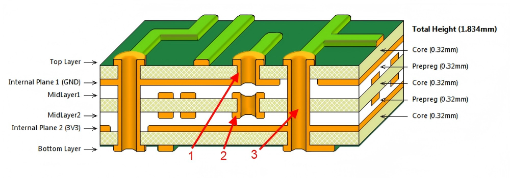
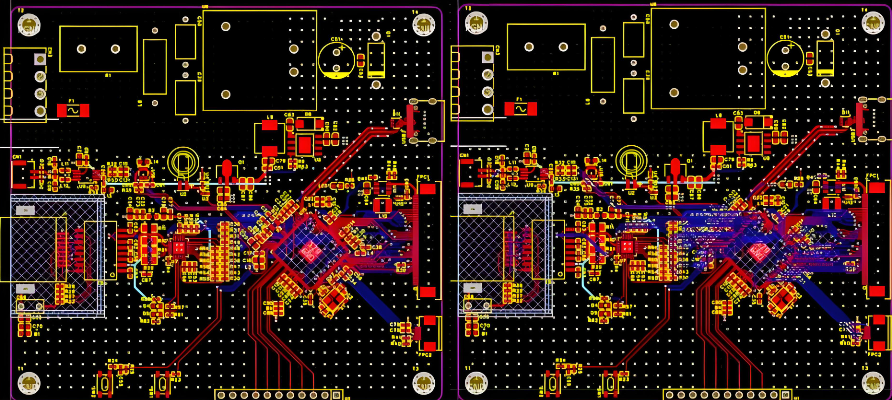
PCB testing refers to structured checks run on printed circuit boards at several key production stages. It makes sure every board meets set design rules, electrical performance needs, and physical durability standards. These checks happen both before and after parts are assembled, covering blank circuit boards, half-finished units, and fully completed products.
Its main purpose is to find defects early, before boards go to full assembly or reach end users. Common small flaws include short circuits, open circuits, poor solder joints, broken wiring traces, and misplaced parts. With consistent targeted testing, these tiny issues never turn into costly failures later on. Good PCB testing also proves boards can handle daily use, normal temperature shifts, and regular wear without breaking down.
On top of catching defects, PCB testing confirms full board function and long-term durability. It ensures each board matches the original design files and works as intended in its final device. This testing works for rigid boards, flexible boards, and rigid-flex hybrid boards alike. No matter the PCB type, consistent testing helps you make reliable products that stand out in competitive markets.
What are the 7 Types of PCB Testing Methods?
Each method targets specific flaws and fits different production stages, creating a full coverage safety net for your boards.
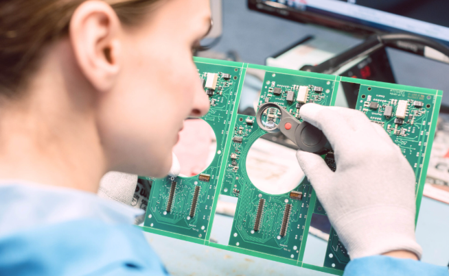
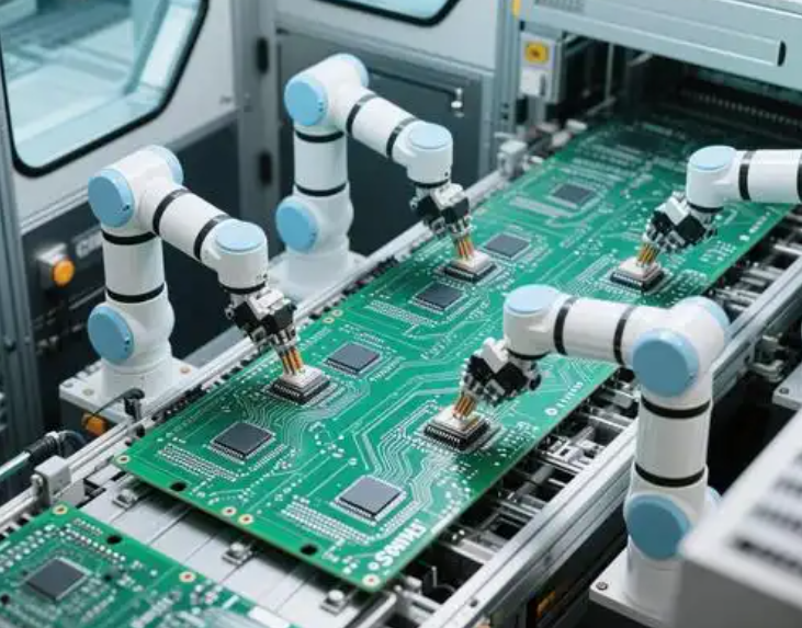
First up is Visual Inspection, the most accessible initial testing step. Trained technicians examine bare boards and assembled units for visible defects like cracked traces, cold solder joints, misplaced components, or damaged substrate material. Many teams pair manual checks with automated optical inspection (AOI) for faster, more precise results. This method catches surface-level issues quickly and keeps early-stage defects from moving forward.
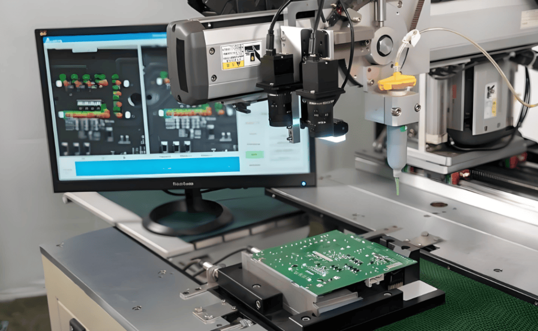
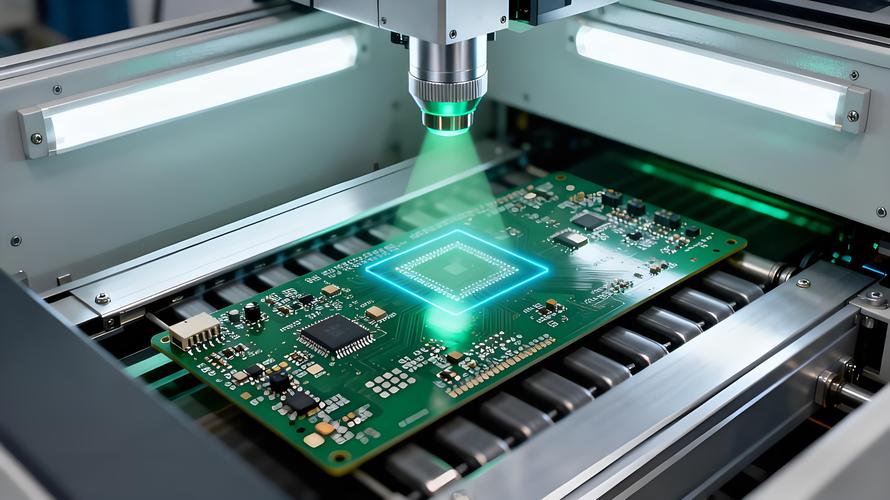
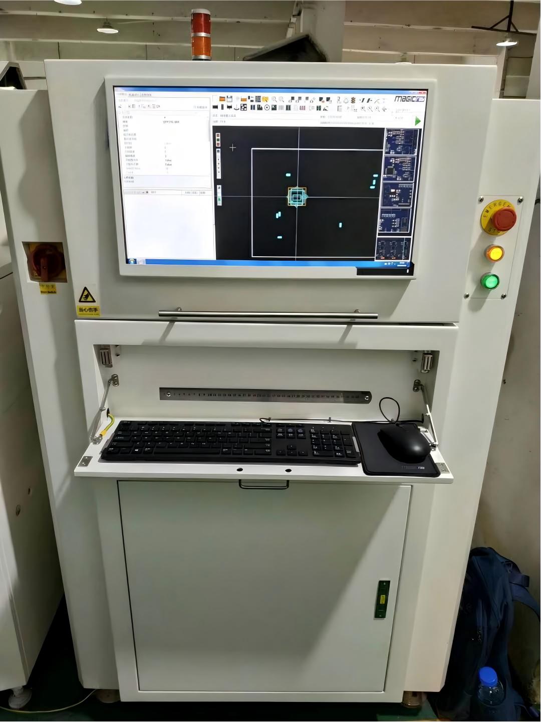
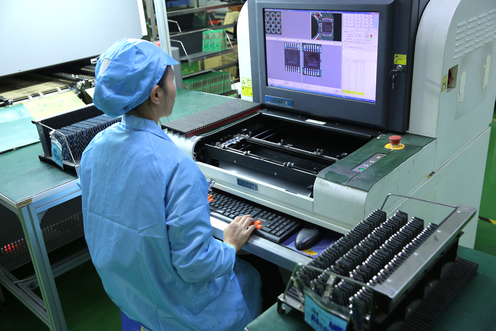
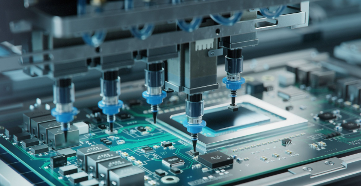
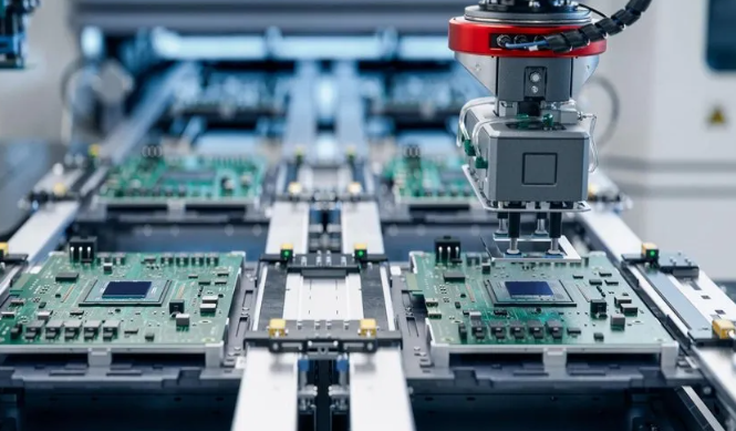
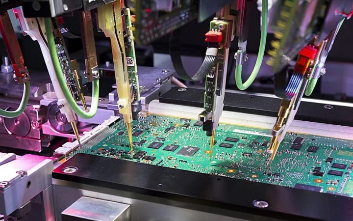
Second is Automated Optical Inspection (AOI), a tech-driven upgrade to manual visual checks. AOI machines use high-resolution cameras to scan PCBs and compare them to digital design files. It spots tiny defects human eyes might miss, such as insufficient solder or shifted micro-components. This method works well for mass production and cuts down on human error significantly.
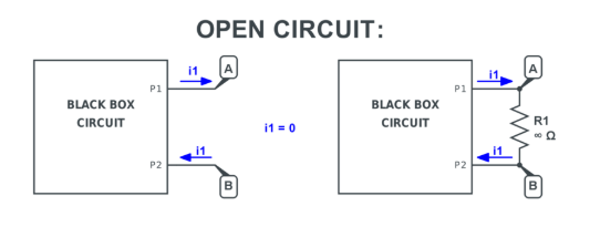
Third is In-Circuit Testing (ICT), which checks individual components and electrical connections on assembled boards. ICT uses a bed of nails fixture to contact specific test points on the PCB. It verifies component values, checks for short or open circuits, and confirms proper part placement. This method delivers fast, accurate results for high-volume production runs.
Fourth is Flying Probe Testing, ideal for low-volume production or prototype boards. Unlike ICT, it uses movable probes instead of fixed fixtures, so no custom tooling is needed. Flying probes test individual points one by one, checking for opens, shorts, and component functionality. It’s cost-effective for small batches and quick prototype validation.
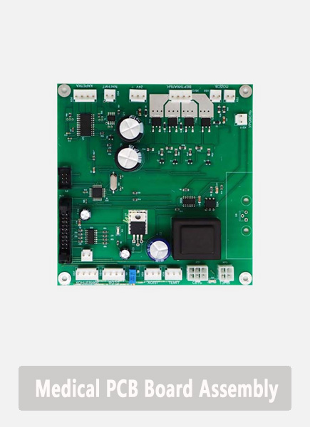
Fifth is X-Ray Inspection, designed for hidden defects that visual checks can’t find. It peer beneath solder joints, ball grid arrays (BGAs), and embedded components. X-ray testing detects cold joints, voids in solder, and internal wiring flaws common in dense, multilayer PCBs. This method is critical for high-complexity boards used in medical and aerospace gear.
Sixth is Functional Circuit Testing, which evaluates the PCB’s full operational performance. Testers power the board and run it through real-world operating conditions to confirm it does its intended job. This test checks overall functionality, not just individual parts, ensuring the board works as a complete unit.
Seventh is Environmental Testing, which checks durability under harsh conditions. Boards undergo temperature cycling, humidity exposure, vibration testing, and shock resistance checks. This ensures PCBs hold up in extreme environments, from industrial factories to outdoor electronic devices.
What are the Most Common PCB Functional Testing Methods?
Building on the customer-focused benefits above, here are the most practical functional PCB testing methods, sorted by production scale, with clear value for your orders and projects.
- Manual Functional Testing: Suited for low-volume orders, custom prototypes and small-batch specialized PCBs. Technicians connect the board to power and test tools, run performance checks manually, and monitor voltage, signals and response speed to confirm full function.
- Automated Functional Testing (AFT): Designed for high-volume mass production. Pre-programmed systems run full performance tests without constant manual oversight, auto-power the board, log test results and finish checks quickly.
- Boundary Scan Testing: Made for dense, high-tech PCBs with limited test points (like BGA and compact surface-mount boards). Uses built-in component circuitry to test connections without direct probe contact.
- Built-In Self-Test (BIST): Integrates auto-diagnostic functions directly into the PCB or its components. The board runs self-checks when powered on, no external test equipment needed.
What are the Benefits of Using PCB Functional Testing Methods?
After covering core PCB testing types, let’s break down the customer-focused benefits of functional PCB testing, with clear, actionable advantages that directly protect your interests and boost your business gains.
- Cut down product failures and after-sales troubles: Functional testing weeds out faulty boards before delivery, so your end customers get fully working PCBs that don’t break down early. This slashes product returns, warranty claims and costly after-sales repairs, and keeps your customers satisfied and loyal for repeat orders.
- Lower your total production costs: It catches defects before finished boards are packaged and shipped, avoiding the high cost of reworking fully assembled units. Less material waste and fewer rework hours add up to big long-term cost savings for your project and business.
- Ensure stable, consistent product quality: Every board you receive meets the same strict performance standards, with zero quality fluctuations between batches. This builds a reliable reputation for your products, and helps you win trust from clients in high-demand, critical industries.
- Speed up order delivery and market launch: Boards pass final checks smoothly and move to shipping quickly, with no delays from last-minute defect fixes. It also eases industry regulatory compliance, as valid functional test results help you get market approval faster.
- Support better product design and fewer recurring flaws: Test data gives clear insights to optimize PCB design and production processes, fixing repeated quality issues. You get more stable, durable boards for future orders, with less risk of consistent defects.
What is the Standard PCB Testing Procedure for Quality Control?
With individual testing methods covered, let’s outline a standard, repeatable PCB testing procedure for consistent quality control. Following this step-by-step workflow ensures no defects slip through the cracks at any production stage.
Step 1: Pre-production design review and test point planning. Before manufacturing starts, engineers mark clear test points on the PCB design for easy access later. This ensures every critical area can be tested efficiently once production begins.
Step 2: Bare board testing on raw substrates. Test for open circuits, short circuits, and trace integrity before any components are added. Fixing flaws at this stage is far cheaper than after assembly.
Step 3: Post-solder inspection right after component assembly. Use AOI or visual checks to spot immediate solder defects before moving to electrical testing. This catches quick fixes early and prevents further processing of faulty units.
Step 4: In-circuit or flying probe testing to check individual components and electrical connections. Verify each part functions correctly and connects to the board as intended.
Step 5: Full functional testing to simulate real-world operation. Power the board and run it through all intended functions to confirm complete performance compliance.
Step 6: Environmental and durability testing for high-reliability applications. Subject boards to stress tests to ensure they hold up in harsh conditions.
Step 7: Final quality check and documentation review. Log all test results for compliance and record-keeping, then approve passing boards for shipping.
This standardized procedure creates a transparent, repeatable system that scales from small prototypes to large production batches. It keeps quality consistent and provides clear documentation for client and regulatory needs.
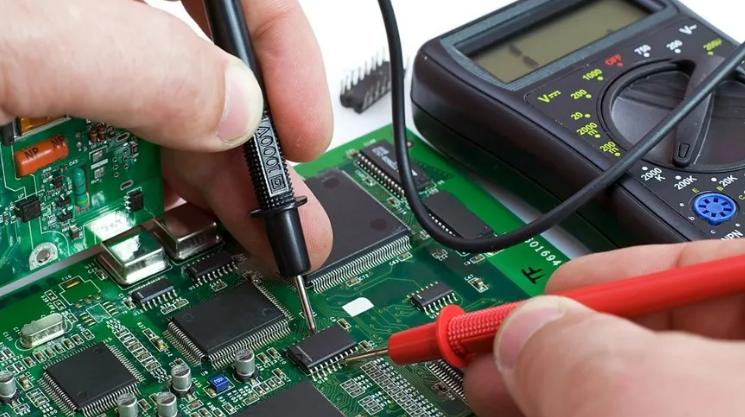
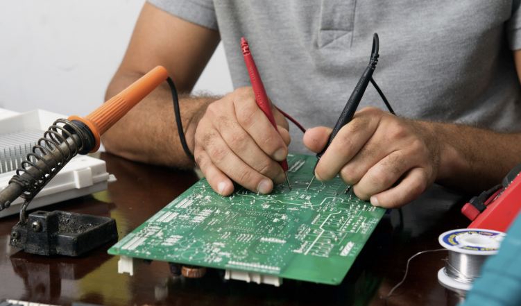
How to Test PCB Board with Multimeter?
For quick, on-the-spot testing without advanced equipment, a multimeter is a reliable and affordable tool. Follow this simple step-by-step guide to test PCBs safely and effectively with a standard multimeter.
First, prepare your workspace and multimeter. Turn off and disconnect the PCB from all power sources to avoid injury or equipment damage. Set your multimeter to the continuity test mode, marked with a sound wave or diode symbol.
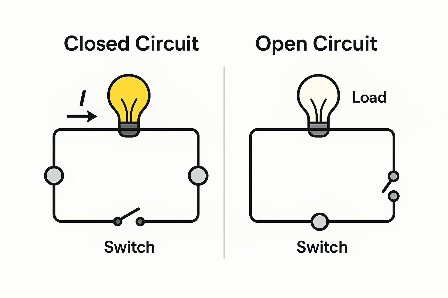
1. Test for short circuits. Touch one multimeter probe to a power trace and the other to a ground trace. A continuous beep means a short circuit is present; no beep means the path is clear.
2. Check for open circuits. Touch both probes to the two ends of a single PCB trace or component lead. A solid beep confirms a closed, working circuit; no beep means an open circuit that needs repair.
3. Test diode and component polarity. Switch the multimeter to diode mode and touch probes to diode leads. Properly functioning diodes show a specific voltage reading in one direction only, confirming correct polarity.
4. Check resistance values for resistors. Set the multimeter to the correct resistance range and touch probes to resistor leads. Compare the reading to the resistor’s labeled value to confirm it functions properly.
5. Verify voltage regulation (for powered boards, only if safe). Once the board is powered correctly, set the multimeter to voltage mode and check voltage at designated test points. Confirm readings match the design specifications for stable performance.
6. Document your findings and mark faulty boards. Log any abnormal readings for repair, and set aside non-functional boards for rework. Always double-check suspicious readings to rule out user error.
This multimeter method is perfect for quick prototype checks, small-batch testing, and field repairs. It’s a handy skill for technicians and engineers working with PCBs in any setting.
What PCB Testing Standards Should Manufacturers Follow?
Following global PCB testing standards ensures consistent quality, cross-market compliance, and predictable performance for every order. These standards set clear, objective rules for testing, defect thresholds, and final product acceptability.
- IPC-A-600: Core standard for bare printed circuit boards; defines clear acceptability criteria for visual and electrical checks. It separates qualified boards from defective ones at the raw substrate stage, preventing flawed blank boards from moving to assembly.
- IPC-J-STD-004: Focused on solder joint quality and assembled PCB testing; sets strict rules for solder joint inspection, rework limits, and final acceptance. It eliminates weak or unreliable solder connections, the top cause of PCB field failures.
- IPC-925: Covers reliability-focused testing and quality compliance protocols; includes environmental testing, durability verification, and long-term performance validation. It ensures boards hold up under real-world stress and extended use.
- ISO 9001: Global quality management standard for full production and testing workflows; ensures consistent, repeatable testing processes across all batches. Compliance proves a commitment to stable quality and continuous process improvement for international markets.
- IPC-6012 (for critical applications): Strict standard for rigid PCBs used in medical, aerospace, and high-reliability industrial devices. It meets tight industry safety and performance rules for products where failure is not an option.
How Do PCB Testing Methods Ensure Quality Control in Production?
Here are PCB testing methods ensure quality control in production:
- Automated Optical Inspection (AOI): Uses high-speed cameras and AI algorithms to detect solder defects, missing components, and alignment errors on PCBs. Ensures visual quality control by identifying surface-level flaws early in production.
- X-ray Inspection: Penetrates PCB layers to inspect hidden solder joints (e.g., BGAs, QFNs) for voids, cracks, or misalignments. Critical for verifying internal quality without physical disassembly.
- Flying Probe Testing (FPT): Employs movable probes to test electrical connections, continuity, and isolation between PCB nodes. Validates circuit functionality and detects open/short circuits with high precision.
- In-Circuit Testing (ICT): Uses fixed test probes to verify component values, polarity, and circuit performance. Ensures all electrical parameters meet design specifications before functional testing.
- Functional Testing: Simulates real-world operating conditions to validate PCB performance under load. Confirms end-to-end functionality, power stability, and signal integrity.
- Boundary Scan (JTAG): Tests digital circuits via IEEE 1149.1 standard to verify connectivity and detect faults in embedded devices. Ideal for complex boards with limited physical access points.
- Thermal Imaging: Monitors heat distribution across PCBs to identify hotspots or cooling issues. Prevents thermal-related failures by ensuring components operate within safe temperature ranges.
- Acoustic Microscopy: Uses high-frequency sound waves to detect delamination, cracks, or voids in PCB substrates. Ensures material integrity and structural reliability.
Whether you’re new to PCB manufacturing or looking to upgrade your existing quality control process, choosing the right PCB testing methods and following consistent procedures makes all the difference. By combining manual checks, automated equipment, and digital software, you can build a robust testing system that delivers reliable, high-performance PCBs every time.