What is LED PCB assembly? Let’s explore its definition, types, applications, assembly steps, how to choose LED PCB assembly service.
Are you troubled with these problems?
- Heat Dissipation Challenges: How can high-power LED PCB assemblies effectively dissipate heat to prevent light decay and shortened lifespan?
- Cost Pressures: How can we reduce material and production costs while ensuring LED PCB assembly quality?
- Design Limitations: How can traditional PCB assemblies achieve flexible adaptation and innovative design in complex lighting scenarios?
EBest Circuit (Best Technology) can provide service and solutions:
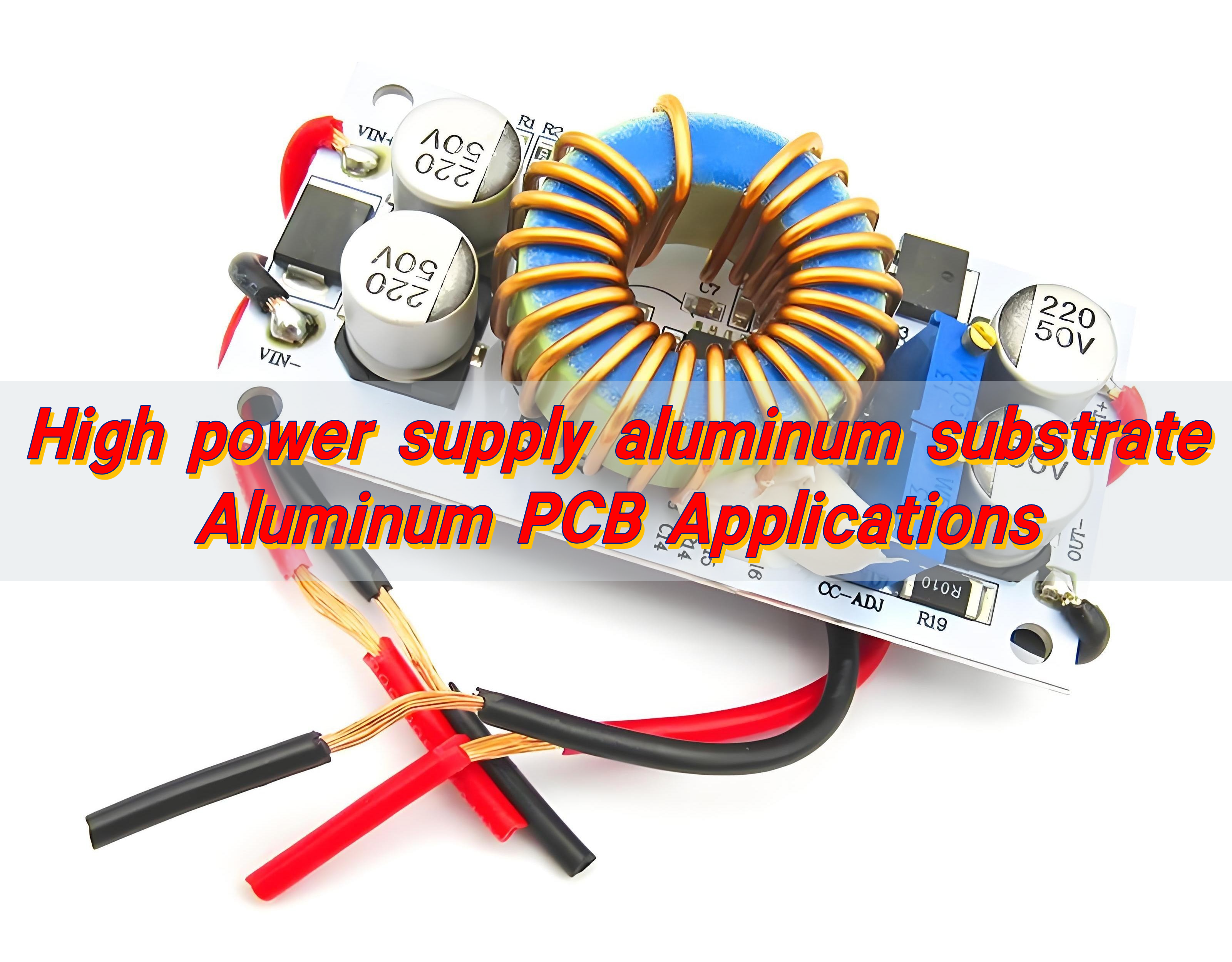
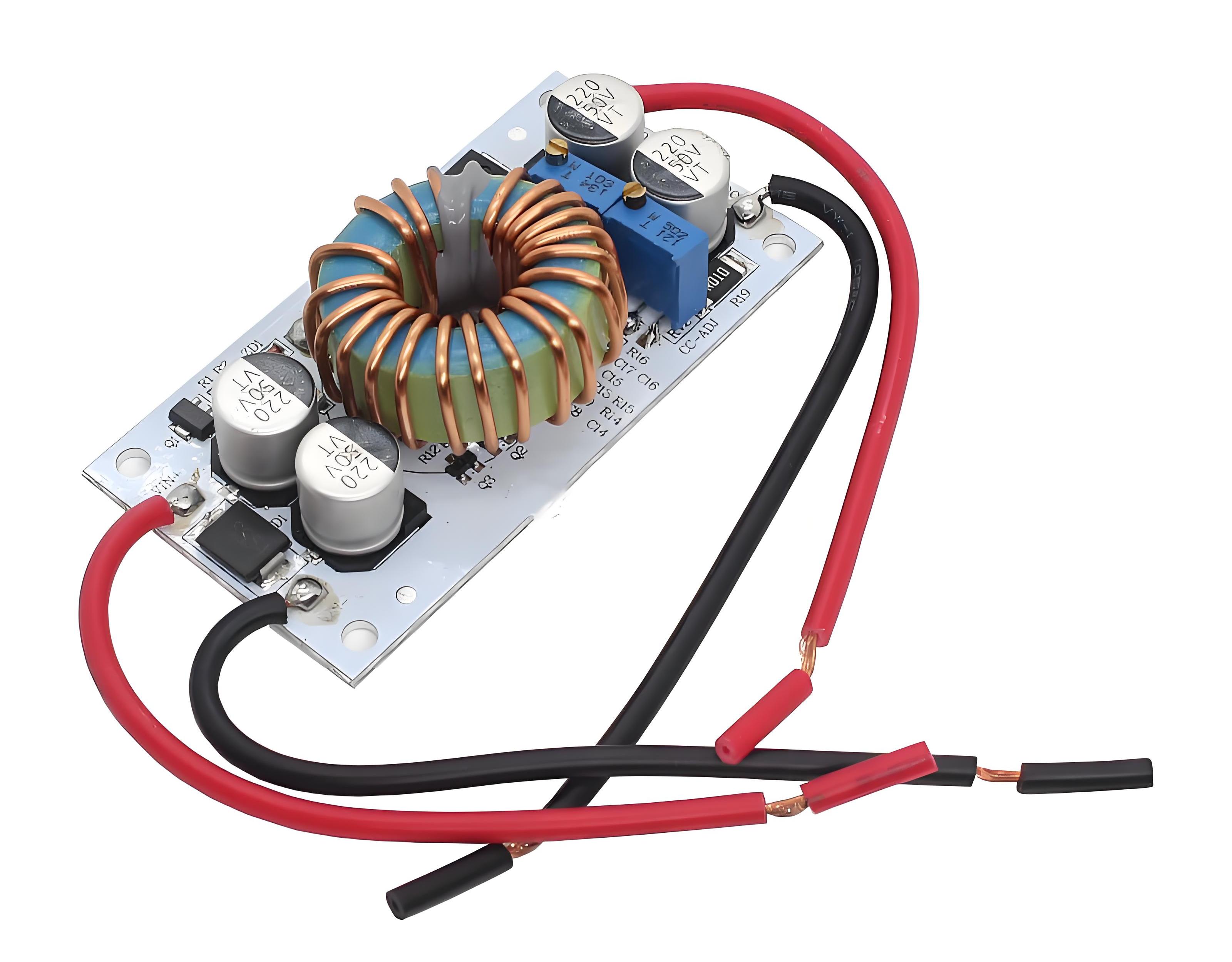
- Efficient Heat Dissipation Solutions: Utilizing highly thermally conductive metal substrates (such as aluminum substrates) and optimized heat dissipation structure design ensures long-term stable operation of LED PCB assemblies, reducing temperatures by over 20%.
- Cost-Optimized Processes: Through refined production management and material selection strategies, we provide customers with cost-effective LED PCB assembly solutions, saving 15%-30%.
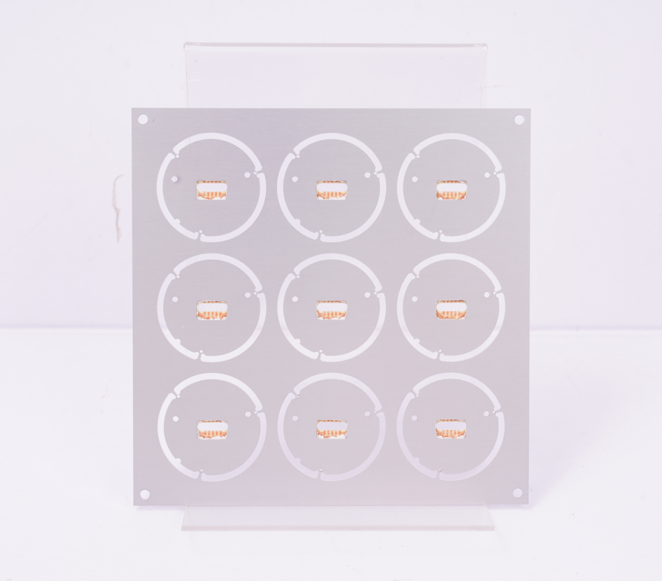
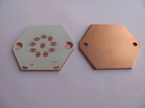
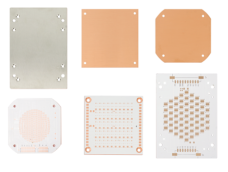
- Customized Design Services: Supporting specialized designs such as custom-shaped boards to meet diverse lighting needs and help customers create differentiated products.
Welcome to contact us if you have any request for LED PCB assembly: sales@bestpcbs.com.
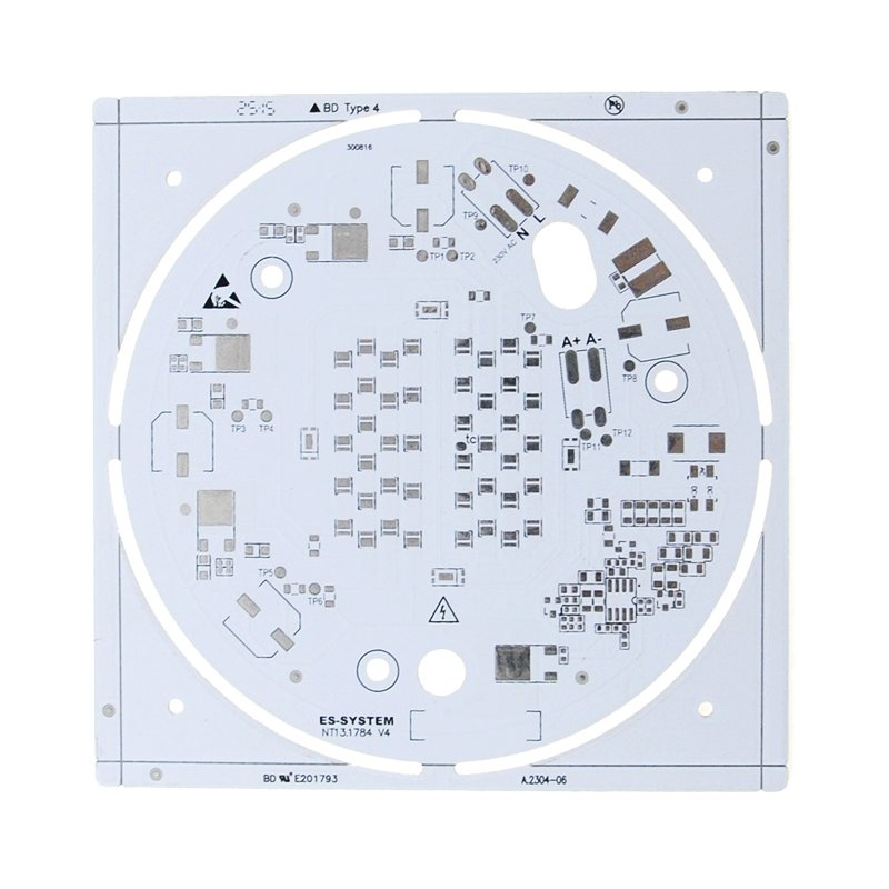
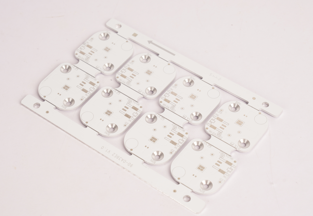
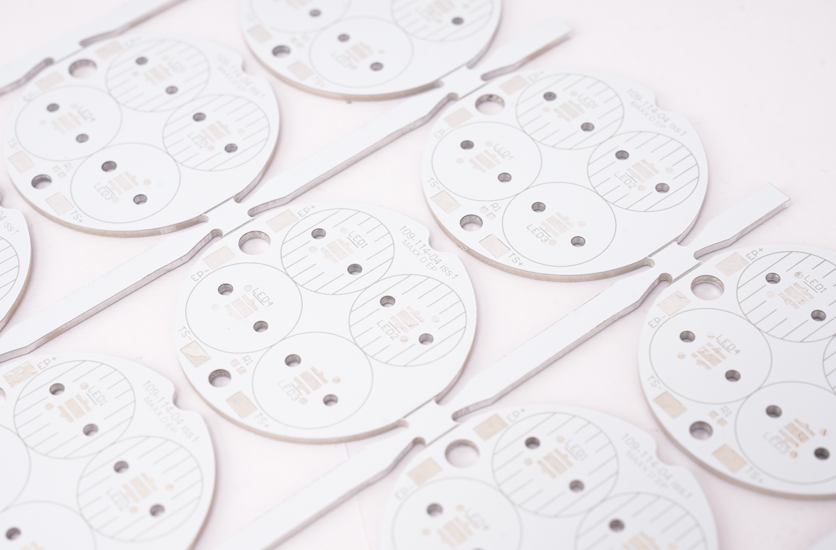
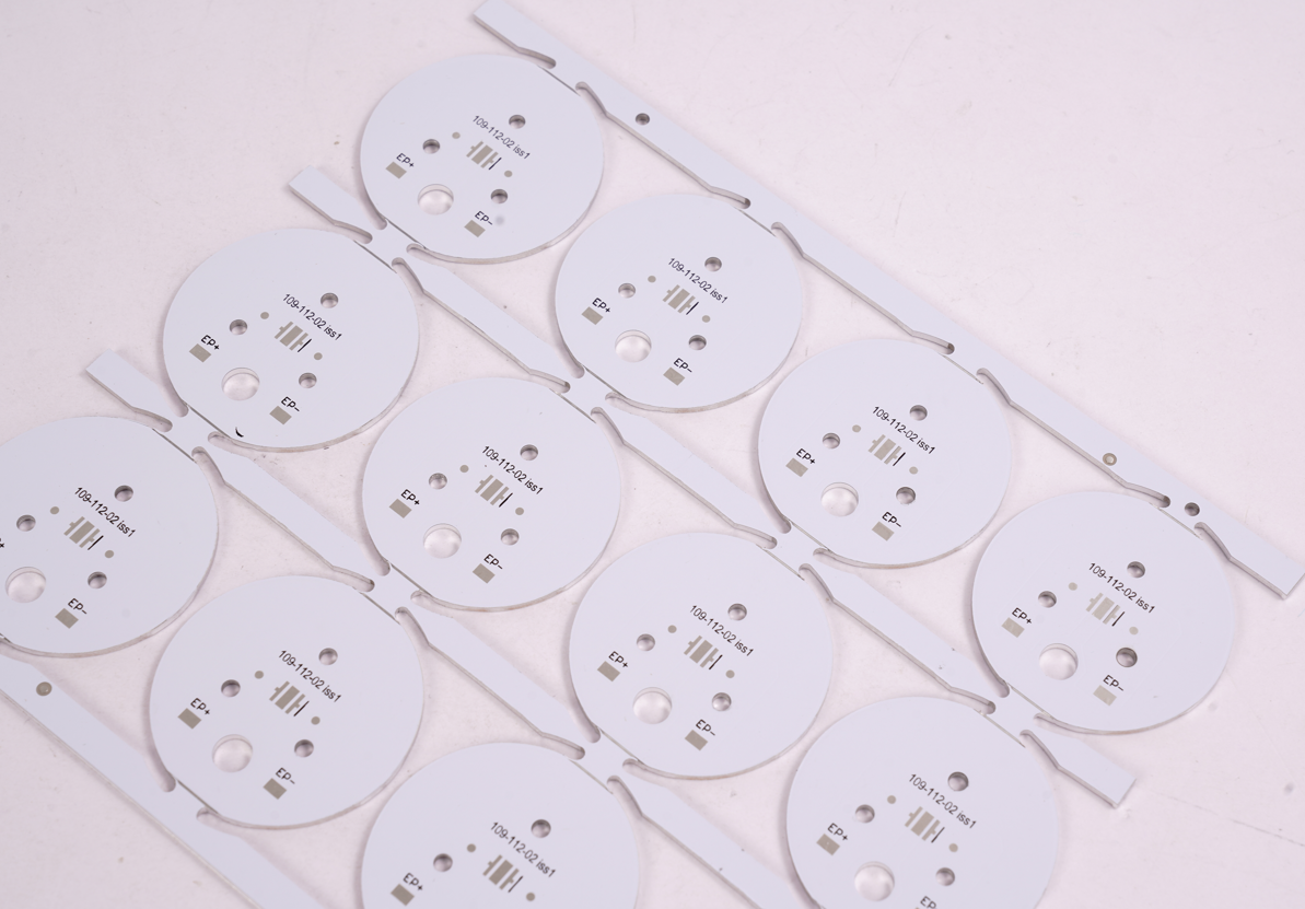
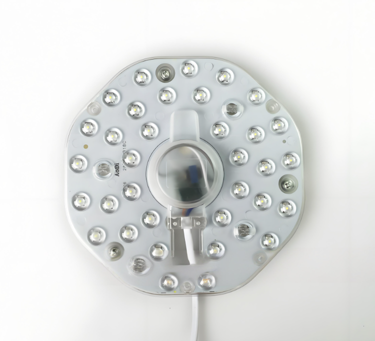
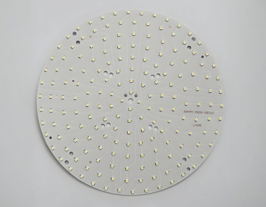
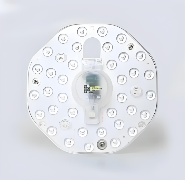
What Is LED PCB Assembly?
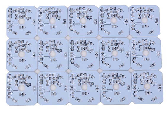
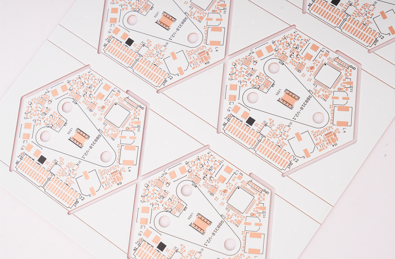
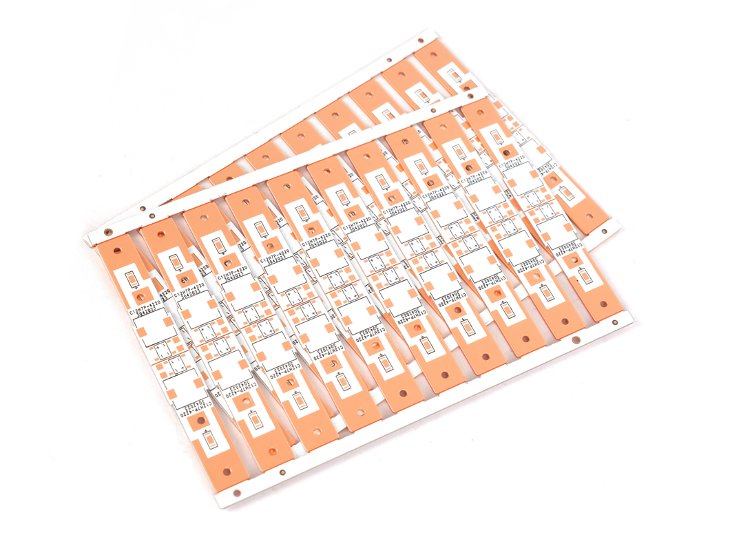
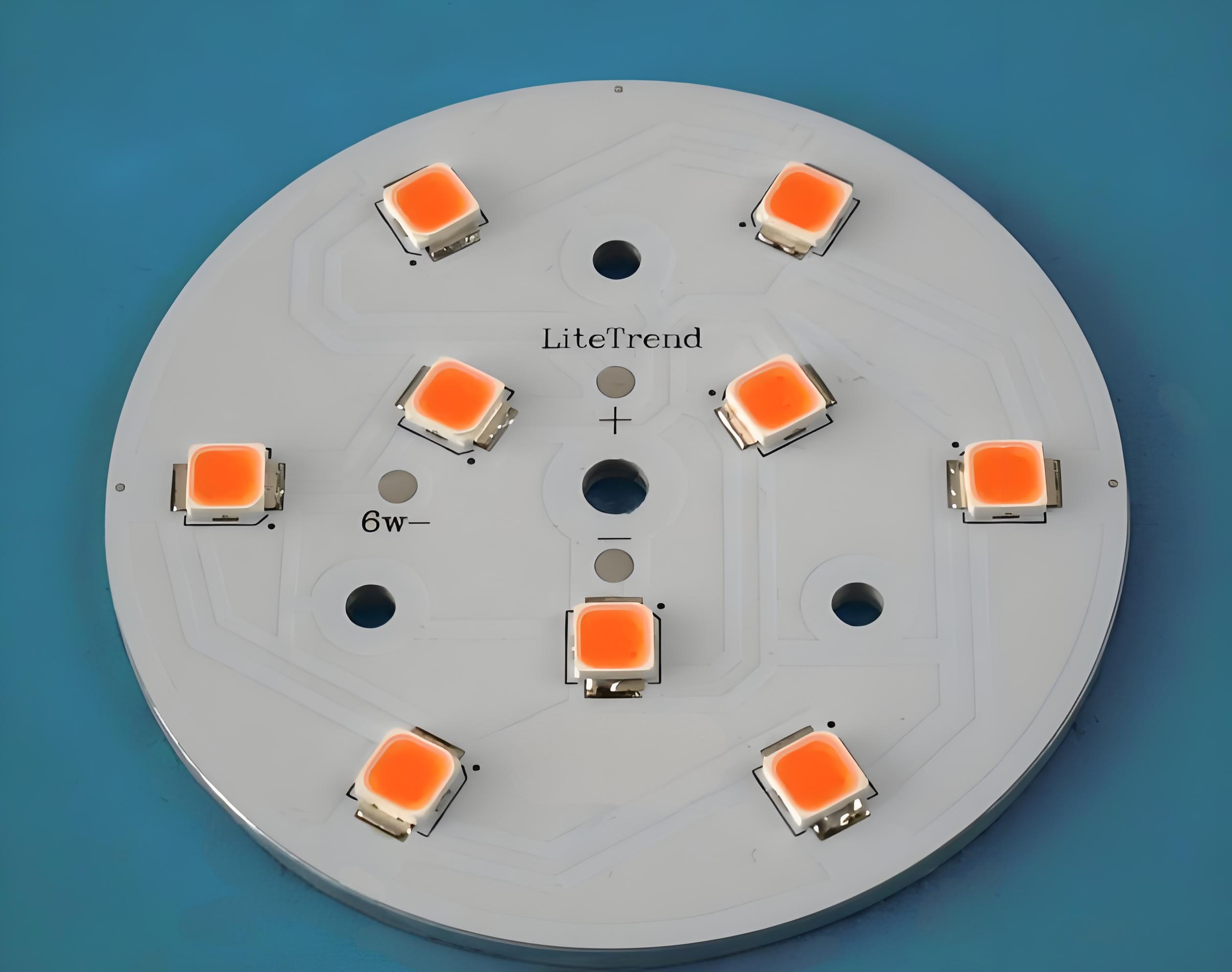
LED PCB assembly refers to the complete manufacturing process of soldering light-emitting diodes (LEDs) and other electronic components onto printed circuit boards (PCBs) using surface mount technology (SMT) or through-hole (DIP) technology. This process includes key steps such as solder paste printing, component placement, reflow soldering, optical inspection, and functional testing. Ultimately, the LED lighting or display module is completed with both electrical connections and physical support. This process requires strict control of soldering quality, heat dissipation, and optical consistency to ensure the reliability and lifespan of the LED product.
Types of LED Lighting PCB Assembly
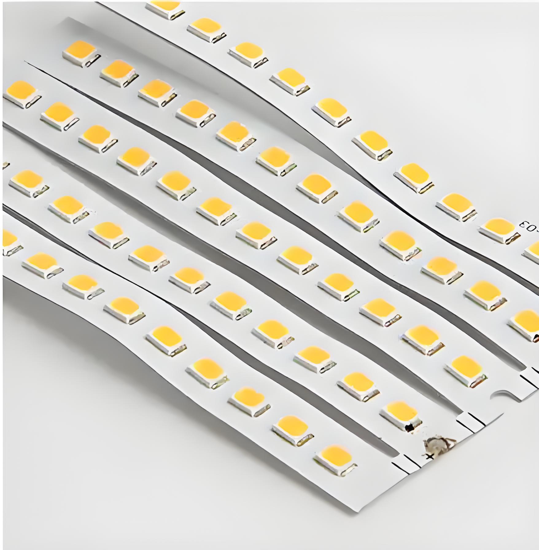
Surface Mount Technology (SMT):
- Definition: LED components are soldered directly onto the PCB surface using a placement machine, suitable for small, high-density designs.
- Advantages: High efficiency, low cost, and support for ultra-thin lighting fixtures (such as light strips and panel lights).
- Applications: Indoor consumer lighting (downlights and spotlights).
Through-Hole Technology (THT):
- Definition: LED pins penetrate PCB holes and are secured by wave soldering. Traditional yet reliable.
- Advantages: High mechanical strength and vibration resistance, suitable for high-power modules (such as street lights and mining lamps).
- Applications: Outdoor and industrial lighting.
Hybrid Assembly (SMT + THT)
- Definition: SMT control chip and THT high-power LED, balancing performance and reliability.
- Advantages: Supports driver circuit integration (such as constant current source), suitable for smart lighting.
- Applications: Smart bulbs, adjustable color temperature lamps.
Applications of LED PCB Assembly
- Commercial/Residential Lighting: High-brightness LED panels (such as downlights and panel lights) with dimming and color adjustment capabilities.
- Stage and Entertainment Lighting: Concert and theater lighting systems (DMX512 protocol control).
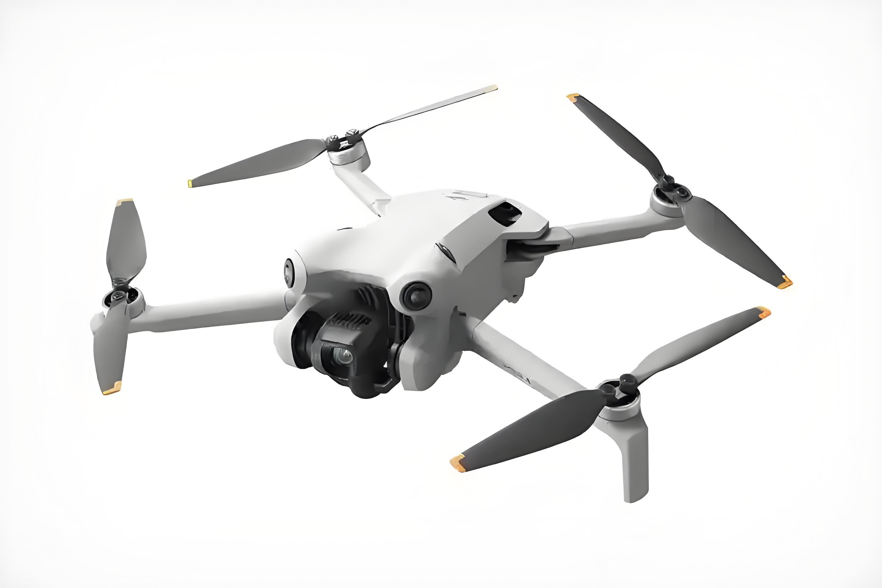
- Automotive Lighting: Headlight modules (daytime running lights, turn signals), instrument panel backlight units.
- Outdoor Displays: Billboards, traffic lights, and stadium display backlight units.
- Medical Equipment: Surgical shadowless lamps, diagnostic instrument indicators, and UV disinfection equipment.
- Industrial Control: Machine vision light sources, safety indicator systems, and automated equipment status displays.
- Consumer Electronics: TV/monitor backlight units, mobile phone flashlights, and wearable device indicators.
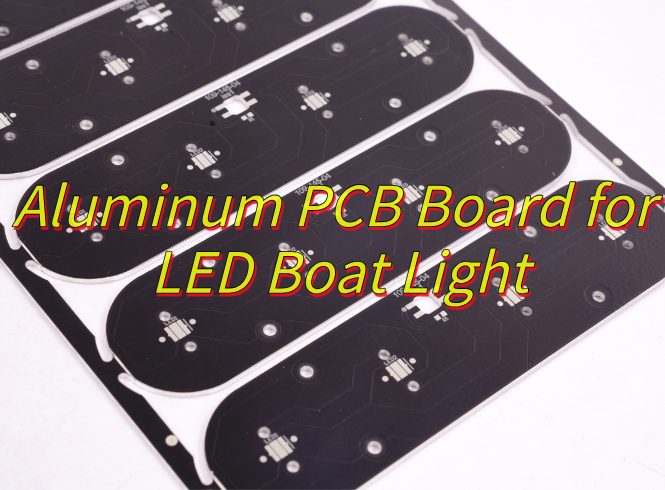
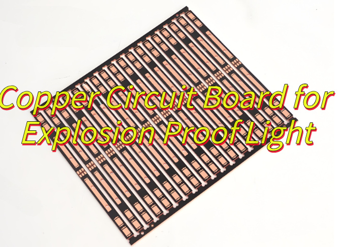
- Special Environment Lighting: Explosion-proof lamps for mining, low-temperature lighting for cold storage, and waterproof light panels for ships.
LED PCB Assembly Process Steps
1. Material Preparation
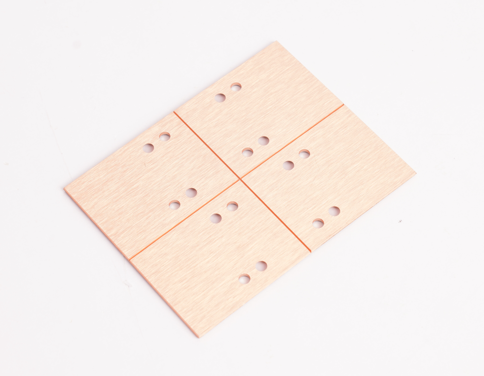
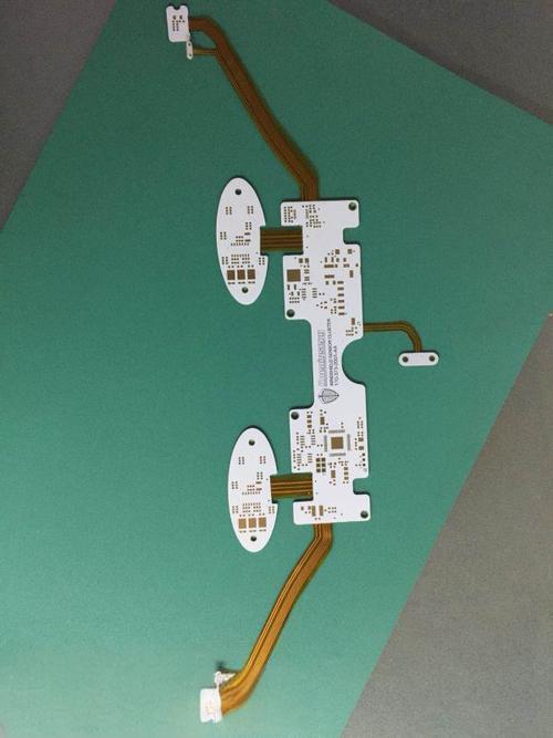
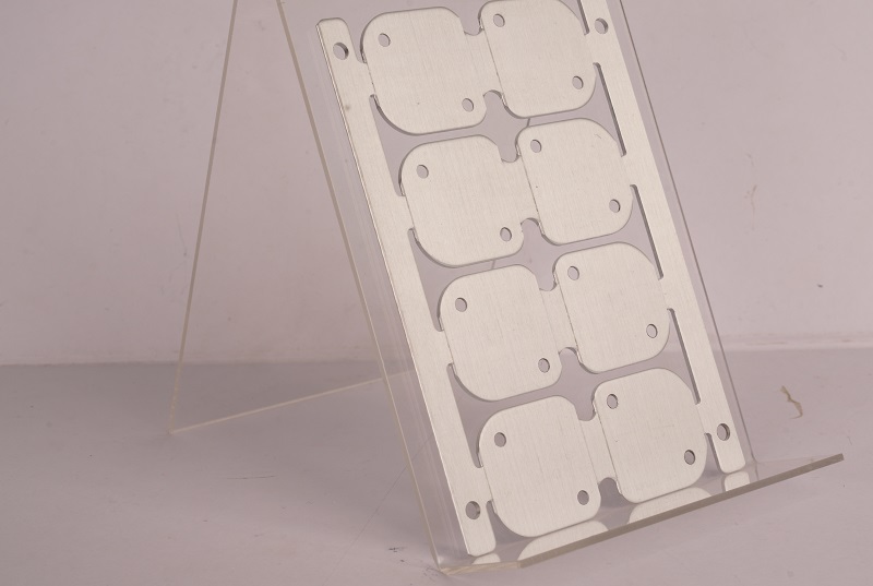
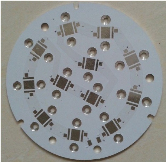
- Cut the substrate (aluminum substrate/flexible board) to size and clean the surface.
- Sort the LED components, resistors, driver chips, etc. according to the bill of materials (BOM).
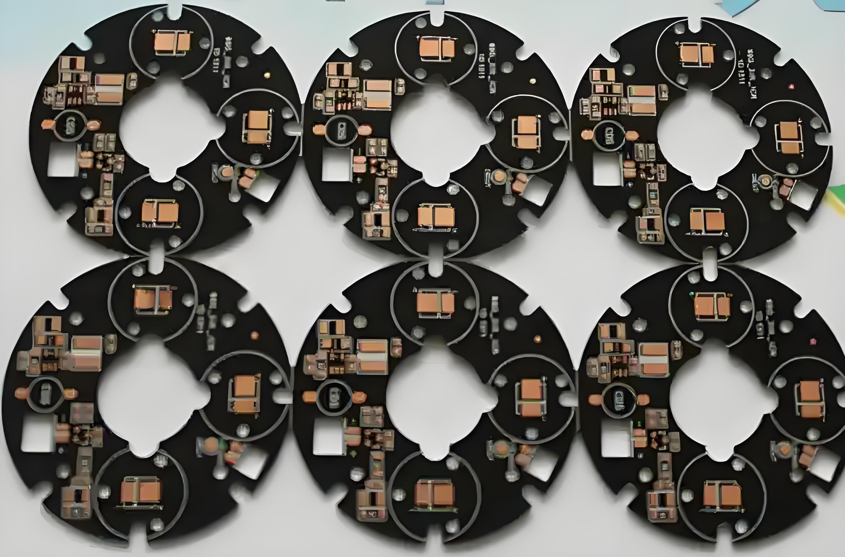
2. Component Placement
- SMT/COB: SMT machine places LED components (accuracy ±0.1mm). COB bonding chips are then coated with phosphor adhesive and cured.
- THT: Insert LED pins into PCB holes using a plug-in machine or manually.
3. Soldering
- SMT/COB: Reflow soldering (220–250°C) ensures full solder joints.
- THT: Wave soldering (260–280°C) ensures a solder fill rate of ≥75% for through-holes.
4. Cleaning and Curing
- Ultrasonic cleaning removes flux, followed by drying (80°C/10 minutes).
- Flexible PCB secondary curing (120°C/2 hours) enhances adhesive adhesion.
5. Electrical Testing
- A multimeter/ICT is used to check LED voltage, resistance, and short/open circuits.
- Drive Circuit Testing: Constant current source accuracy of ±3%, dimming function verification.
6. Optical and Thermal Testing
- An integrating sphere is used to measure luminous efficacy (lm/W), color temperature (±100K), and color rendering index (Ra ≥ 80).
- A thermal imager is used to monitor LED junction temperature rise (≤ 85°C).
7. Aging Quality Inspection
- 72 hours of continuous aging (rated power/60°C), eliminating modules with a lumen decay of ≥ 5% or faults.
- Appearance Inspection: Smooth solder joints and no deformation of the substrate.
8. Packaging:
- Packaged in an anti-static bag, with parameters (power, color temperature) and safety certifications marked.
- A test report (luminous efficacy, temperature rise, aging data) and installation instructions are included.
What Should You Look for When Choosing LED PCB Assembly Service?
Process Compatibility & Technical Expertise
- Support for SMT, COB, THT, flexible PCB, and hybrid assembly processes to accommodate diverse LED products (e.g., high-density light strips, high-power streetlights).
- Precision equipment: placement accuracy ≥ ±0.05mm, reflow soldering temperature control (220–250°C), wave soldering (260–280°C) for reliable joints.
- Thermal simulation (ANSYS/FloTHERM), DFM optimization, and BOM standardization to preempt design flaws (e.g., pad orientation aligned with panelization to prevent wire bonding damage).
Quality Control & Inspection Protocols
- Adherence to IPC-A-610 standards, with AOI, X-ray inspection (solder joint void rate ≤5%), and ICT for electrical performance verification.
- Environmental testing: thermal shock (-40°C~125°C/1000 cycles), 85°C/85%RH humidity resistance (1000 hours), and aging tests (72-hour continuous operation, ≤5% lumen degradation).
- Full material traceability, ensuring RoHS/halogen-free compliance and waste management practices.
Certifications & Regulatory Compliance
- ISO 9001 certification for quality management; IATF 16949 (automotive) or ISO 13485 (medical) for industry-specific compliance.
- Use of lead-free solder, eco-friendly substrates, and third-party environmental reports.
Production Capacity & Delivery Efficiency
- 24-hour prototype turnaround, small-batch production (48-hour lead time), and monthly output ≥100,000 sq.ft.
- Multi-modal logistics (air/ground freight) with ≥95% on-time delivery; BOM sourcing and consignment stock support.
Industry Experience & Client References
- Proven expertise in automotive, medical, and smart home sectors with tailored solutions (e.g., modular designs, thermal management optimization).
- Partnerships with Tier 1 suppliers or automotive OEMs (e.g., Ford, Toyota); case studies demonstrating defect resolution (e.g., solder paste curing issues, low-temperature solder cracking).
Cost Optimization & After-Sales Support
- Transparent pricing with BOM cost breakdowns and customizable quotation structures.
- Cost-saving strategies: material substitution (e.g., embedded heat pipes vs. thick copper) and process improvements (e.g., hybrid assembly for labor reduction).
- 24/7 failure analysis, rapid replacement, and NDA-backed design confidentiality.
Why Choose EBest Circuit (Best Technology) as LED PCB Assembly Manufacturer?
Reasons why choose us as LED PCB assembly manufacturer:
- Competitive Pricing: Our direct supply model eliminates middlemen, reducing bulk order costs by 15%-20% with no hidden fees.
- Environmentally Friendly Materials and Processes: Utilizing 25% recycled aluminum and lead-free processes, we comply with RoHS/REACH standards and reduce raw material costs.
- 24-Hour Rapid Prototyping: LED PCB samples are delivered within 24 hours, shortening the development cycle for a stage lighting project by 50%.
- Quality Certification: ISO 9001/IATF 16949/ISO 13485 certified, making us suitable for demanding applications such as medical and automotive.
- Strict Quality Control: 100% automated inspection with Automated Optical Inspection (AOI) ensures a solder joint defect rate of <0.01%, extending the LED board lifespan to over 50,000 hours.
- Free Design for Function (DFM) Optimization: Pre-review design files to identify issues such as insufficient thermal vias and close copper spacing, reducing design revisions and development costs by 30%.
- Turnkey Solution: This one-stop service covers the entire process, including PCB layout (compatible with Altium/PADS), thermal simulation (ANSYS Icepak), and SMT assembly.
- 24/7 engineering response: Thermal runaway and EMC interference issues are resolved within an average of 4 hours, ensuring zero downtime for on-site projects.
Our LED PCB Assembly Capabilities
| Item | Capabilities |
| Placer Speed | 13,200,000 chips/day |
| Bare Board Size | 0.2 x 0.2 inches – 20 x 20 inches/ 22*47.5 inches |
| Minimum SMD Component | 01005 |
| Minimum BGA Pitch | 0.25mm |
| Maximum Components | 50*150mm |
| Assembly Type | SMT, THT, Mixed assembly |
| Component Package | Reels, Cut Tape, Tube, Tray, Loose Parts |
| Lead Time | 1 – 5 days |
How to Get a Quote for LED PCB Assembly Service?
LED PCB Assembly Quote Required Documents
1. Design Files:
- Gerber Format PCB Layout File + Bill of Materials (BOM) (including component specifications)
2. Technical Specifications:
- PCB Layer Count, Dimensions, and Copper Thickness Requirements
- Surface Finish (HASL/ENIG/OSP)
- Special Requirements (e.g., thermal via design, impedance control)
3. Order Information:
- Estimated Quantity (Sample/Small Batch/Mass Production)
4. Delivery Time Requirements
- Certification Requirements (if applicable): RoHS/REACH, ISO, IATF 16949, etc.
Why Choose EBest Circuit (Best Technology)?
- Free DFM: Identify design risks early and reduce development costs
- Transparent Quotation System: No hidden fees, 15%-20% cost savings for bulk orders
- Full Process Control: From PCB manufacturing to SMT assembly, one-stop service
Get Started Now! Welcome to contact us if you have any inquiry for LED PCB assembly: sales@bestpcbs.com.