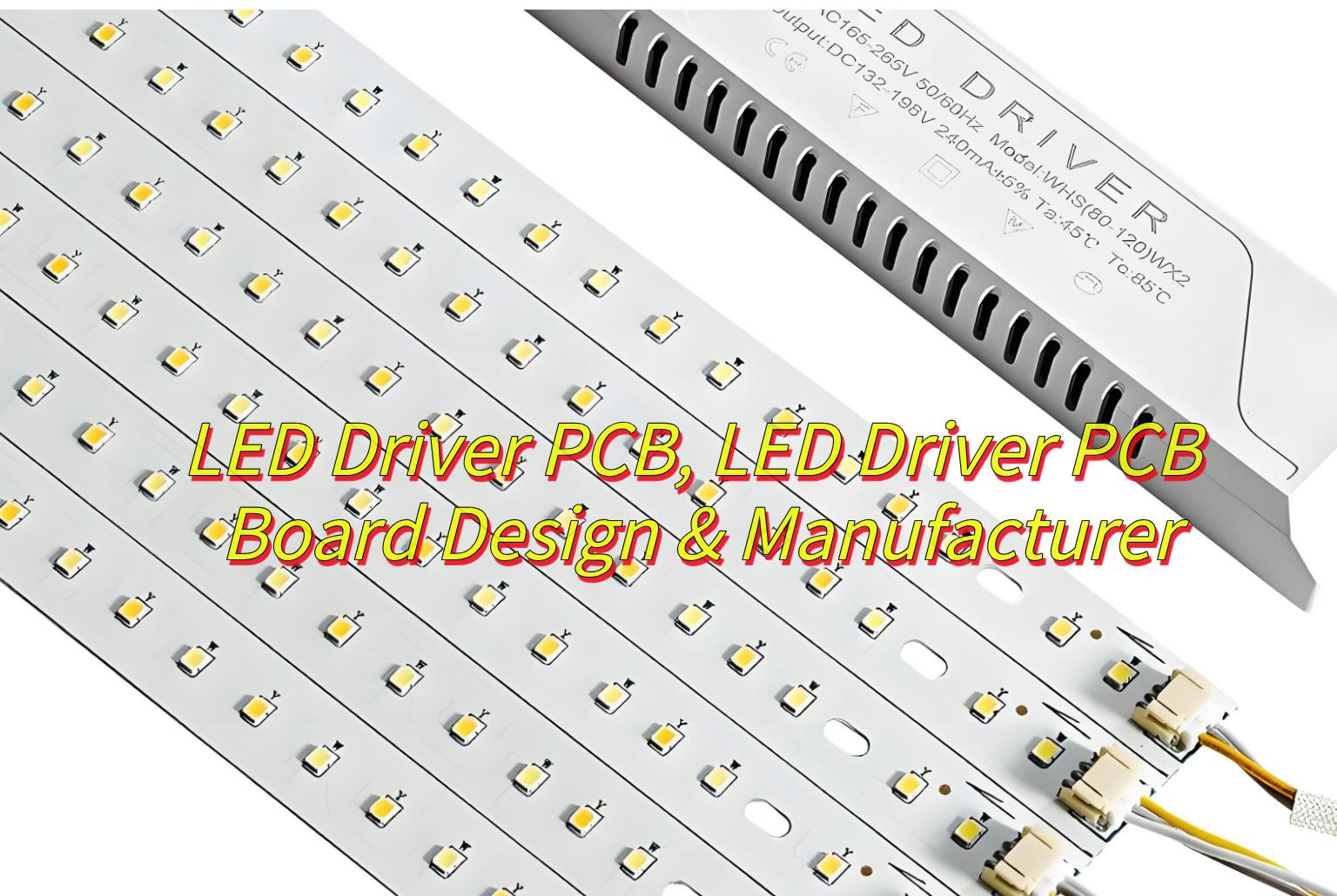
Are you looking for a LED Driver PCB manufacturer with design service? Let’s explore more about how to design LED driver PCB and how to select a reliable LED driver PCB manufacturer.
At EBest Circuit (Best Technology), we focus on LED driver PCBmanufacturing and designing over 18 years. We prioritize IP Protection & NDAs, ensuring your designs are safeguarded through strict confidentiality agreements and secure data handling. And we maintain Quality & Compliance with certifications like ISO 9001, UL, and CE, guaranteeing adherence to the highest industry standards and safety regulations. Then we can provide 48 hours rapid prototyping service because we have stable electronic supply chain. If you have any request for LED driver PCB board, please feel free to contact us: sales@bestpcbs.com
What Is LED Driver PCB?
An LED driver PCB is a printed circuit board specifically designed to control and regulate the power supplied to LEDs. It converts incoming electrical power (e.g., AC mains or DC sources) into the precise voltage and current required by the LEDs, ensuring stable operation, brightness consistency, and protection against voltage fluctuations or overheating. Key components on the board include voltage regulators, current controllers, and thermal management elements like heat sinks. LED driver PCBs are critical in applications like residential/commercial lighting, automotive headlights, and digital displays, as they optimize energy efficiency, extend LED lifespan, and enable features like dimming or color control.
What Advantages of Power LED Driver PCBs Board?
Here are five main advantages of a Power LED Driver PCB:
High Efficiency and Energy Saving-Optimized power topologies (e.g., Buck, Boost, LLC resonant circuits) deliver efficiency up to 90%+, minimizing energy waste.
Stable Current Regulation-Advanced control algorithms maintain precise LED current across wide input voltage ranges (e.g., 90–264Vac), ensuring consistent illumination.
Compact and Integrated Design-High-density component placement and SMD technology reduce PCB size, enabling sleek, space-efficient lighting solutions.
Robust Thermal Management-Multi-layer PCBs with thermal vias and copper heat sinks efficiently dissipate heat, enhancing reliability in high-temperature environments.
Electromagnetic Compatibility (EMC)-Compliance with international EMC standards (e.g., IEC/EN 55015) minimizes electromagnetic interference, ensuring seamless integration into smart systems.
Begin with a topology like Flyback or LLC resonant. Use design tools (e.g., Altium, Eagle) to create a schematic, ensuring components (MOSFETs, capacitors, inductors) are rated for 100W.
2.Component Selection
Choose high-efficiency MOSFETs, capacitors (e.g., electrolytic, ceramic), and inductors. Verify their current, voltage, and thermal ratings for 100W operation.
3.Thermal Management
Integrate heat sinks, thermal pads, and vias into the PCB layout to efficiently dissipate heat from power components.
4.PCB Layout & LED Driver PCB Schematic
Place power components close together to minimize high-current trace lengths.
Use wide traces (e.g., 2–3mm) for power delivery to avoid voltage drop.
Separate power, ground, and control signals in a multilayer stack-up.
5.EMI/EMC Compliance
Add input/output filters, shielding, and proper grounding to meet EMI/EMC standards (e.g., CISPR 32, FCC Part 15).
6.Prototyping & Testing
Fabricate a prototype based on the LED driver PCB schematic and test for efficiency, thermal performance, and EMI compliance.
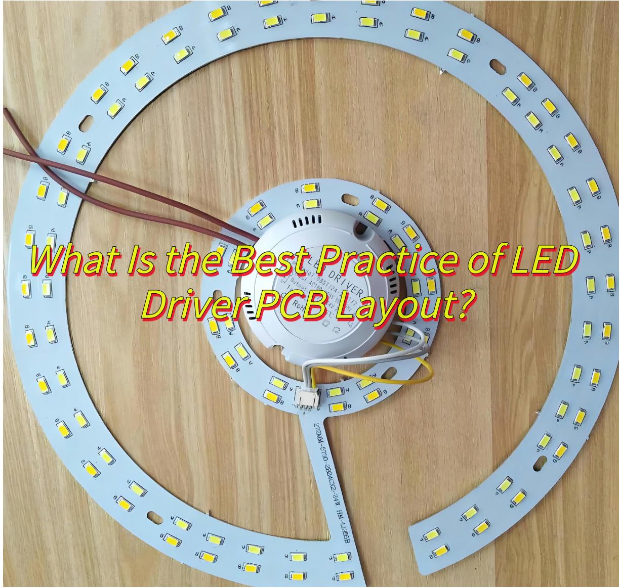
What Is the Best Practice of LED Driver PCB Layout?
Here’s a streamlined guide to LED driver PCB layout best practices:
Component Placement Cluster power transistors, capacitors, and inductors to shorten high-current traces and minimize inductance.
Thermal Management Locate heat-sensitive components (e.g., MOSFETs, ICs) near cooling solutions. Use thermal vias to efficiently conduct heat away.
Ground Plane Design Maintain a solid, unbroken ground plane to reduce EMI and ensure clean signal returns.
Trace Width Sizing Calculate trace widths based on current load (e.g., 1mm per 1A) to prevent voltage drop and overheating.
Layer Stack-up Isolate power, ground, and signal layers in multilayer boards to minimize cross-talk and noise.
What Are Custom Solution For 10W RGB LED Driver PCB?
Here’s a concise guide to custom solutions for a 10W RGB LED driver PCB:
Color Control Interface Implement PWM or analog control for precise RGB color mixing and dynamic lighting effects.
Current Regulation Use constant-current drivers for each RGB channel to maintain color accuracy and LED lifespan.
Dimming Compatibility Design for compatibility with PWM, TRIAC, or 0-10V dimming systems to suit diverse applications.
Compact Design Optimize PCB layout for a small form factor, using SMD components and efficient thermal management.
Protection Features Include over-current, over-temperature, and short-circuit protection to enhance reliability.
How Is A Round LED Driver PCB Manufactured?
The production of round LED driver PCBs follows a specialized workflow to accommodate their unique geometry while maintaining electrical integrity. Below is the streamlined manufacturing process:
Copper Clad Laminate Cleaning: Clean circular substrates (e.g., FR-4) to remove contaminants like dust or oxidation, ensuring adhesion for subsequent processes.
Dry Film Lamination: Apply photosensitive dry film to the copper layer, followed by UV exposure through a circular mask to define the circuit layout.
Development & Etching: Remove unexposed dry film using alkaline solutions; Etch away unprotected copper with ferric chloride or ammonium persulfate, forming conductive traces.
Alignment & Pressing: Align multiple circuit layers (for multi-layer designs) using alignment holes, then bond them under high temperature and pressure with prepreg resin.
Mechanical Drilling: Use CNC machines to drill holes for vias and component mounting, maintaining precision to avoid radial deviations.
Electroless Copper Deposition: Deposit a thin copper layer on hole walls to establish electrical connectivity between layers.
Outer Layer Shaping: Cut the PCB into a circular shape using CNC routers with diamond-coated bits. Fixtures ensure centering accuracy and smooth edges.
Solder Mask: Spray or screen-print epoxy-based solder mask, leaving exposed pads for soldering.
Surface Treatment: Apply HASL (Hot Air Solder Leveling) or ENIG (Electroless Nickel Immersion Gold) to prevent oxidation and enhance solderability.
Testing: Automated Optical Inspection (AOI): Scan for defects like open/short circuits using high-resolution cameras.
Silkscreen Printing: Add component labels or logos using UV-curable ink.
Packaging: Seal in anti-static bags with desiccants to prevent moisture damage during transit.
How to Choose A Reliable LED Driver PCB Board Manufacturer?
IP Protection & NDAs-Partner with manufacturers who prioritize intellectual property protection by signing NDAs and implementing secure design safeguarding measures.
Rapid Production Cycles-Prioritize manufacturers with streamlined processes for quick prototyping and fast production turnaround times to meet urgent deadlines.
Quality & Compliance-Choose manufacturers holding certifications like ISO 9001, UL, or CE, ensuring adherence to quality standards and safety regulations.
Design Expertise-Select a manufacturer with proven experience in LED driver PCB design, including efficient thermal management, EMI compliance, and optimized layouts.
Premium Materials & Components-Ensure they use high-quality, application-specific materials and components to guarantee performance and longevity.
How to DIY 8W LED Driver PCB?
Here’s a simplified guide to DIY an 8W LED driver PCB:
Design the Circuit Use software like EasyEDA or KiCad to design your 8W LED driver circuit, ensuring proper component selection and layout.
Choose Components Select an appropriate LED, driver IC, resistors, capacitors, and a power supply rated for 8W output.
Create PCB Layout Design the PCB layout with component placement and trace routing optimized for your circuit.
Manufacture the PCB Order the PCB from a fabricator or etch it yourself using a photoresist and etching solution.
Assemble Components Solder all components onto the PCB, following the circuit diagram.
Test the Driver Power up the PCB and test its functionality, ensuring it delivers the correct voltage and current to your LED.
In conclusion, that’s all about LED driver PCB board designing and manufacturing. if you have any issues with LED driver PCB board, please leave a message below this blog.
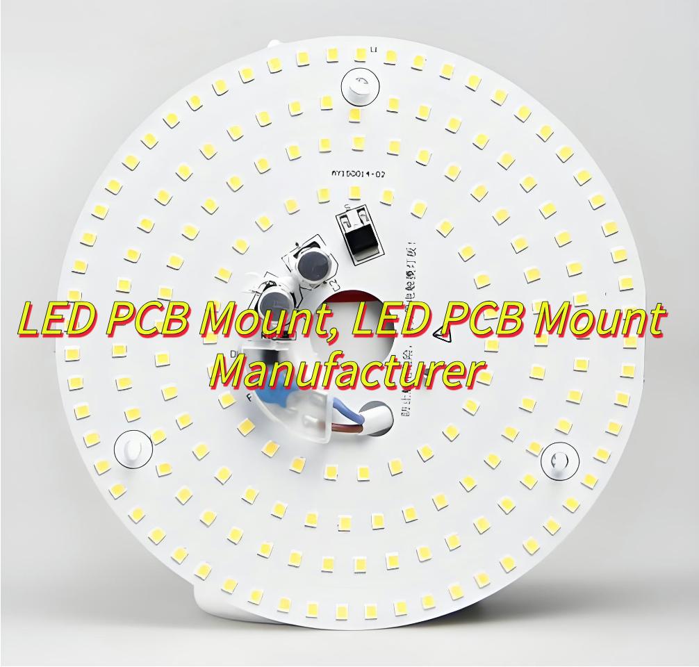
Are you looking for a good LED PCB Mount service? In this blog, Let’s learn the types, infrared benefits, automated solutions of LED PCB Mount, and tips for choosing LED PCB Mount manufacturers.
Choose EBest Circuit (Best Technology) for your LED PCB mount needs. We excel in premium material selection, offering thermally optimized solutions tailored to your requirements. Our state-of-the-art engineering ensures ±0.05mm tolerances, guaranteeing seamless LED integration and superior heat dissipation. Rigorous thermal testing and simulations validate every design, ensuring peak performance. Compliant with UL, CE, and RoHS standards, our solutions meet global safety and environmental benchmarks. Plus, our scalable production and responsive support make us the ideal partner for projects of any size. Contact us today for a quote: sales@bestpcbs.com
What is LED PCB Mount?
An LED PCB mount refers to a light-emitting diode (LED) designed to be securely attached to a printed circuit board (PCB). These components are integral to modern electronics, combining the LED’s light-generating capabilities with the PCB’s ability to provide electrical connections, structural support, and thermal management.
What Are the Types of LED PCB Mounting?
LED PCB mountingmethods vary by technical approach, each suited to specific needs:
Through-Hole (DIP)-LEDs mounted via pins in drilled PCB holes; manual assembly, low cost, suited for basic indicators.
Integrated Modules-Pre-built units with LEDs, drivers, and optics; plug-and-play for smart lighting/IoT systems.
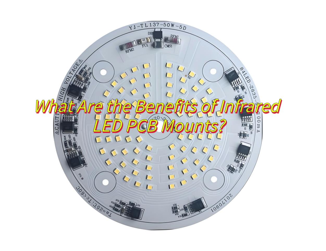
What Are the Benefits of Infrared LED PCB Mounts?
Superior Heat Dissipation: Metal-core PCBs (e.g., aluminum) manage high heat from IR LEDs, ensuring stable performance and extended lifespan in thermal-sensitive applications.
Robust Performance in Harsh Environments: Durable mounting (e.g., SMT/COB) and corrosion-resistant materials withstand vibrations, humidity, and extreme temperatures for industrial/outdoor use.
Miniaturized Design & Scalability: SMT enables compact, high-density layouts for space-constrained devices, while automated production cuts costs for mass-market adoption.
High Signal Consistency: Precision mounting minimizes electrical noise, ensuring reliable IR output for communication (e.g., remote controls, LiDAR).
Customizable Optical Output: Tailored PCB designs optimize wavelength focus (e.g., 850nm/940nm) for biometrics, surveillance, or medical systems.
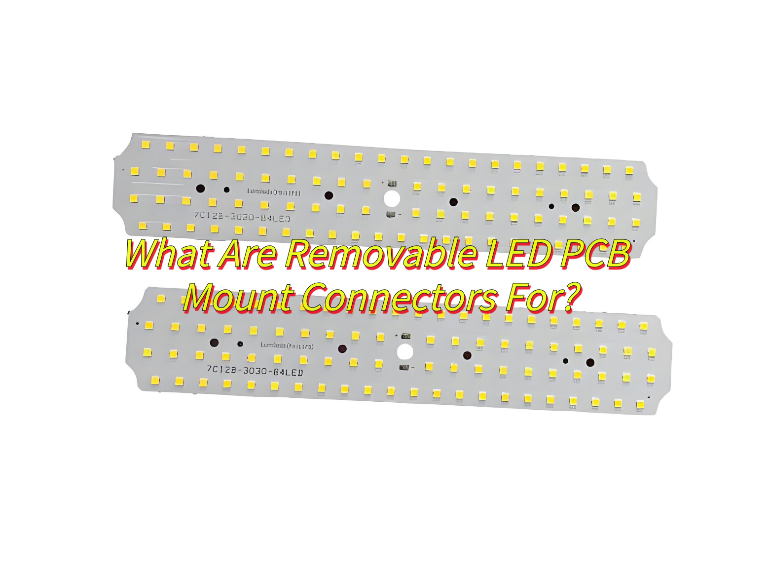
What Are Removable LED PCB Mount Connectors For?
Modular Maintenance & Upgrades-Replace or upgrade LED modules without soldering, drastically reducing system downtime.
Flexible System Design-Reconfigure LED layouts (color, brightness) by swapping modules, adapting to dynamic needs.
Hot-Swappable Reliability-Replace faulty units during operation, ensuring continuous performance in critical applications.
Simplified Inventory-Standardize connectors across products to minimize stock complexity and costs.
Cost-Efficient Repairs-Fix issues by replacing only damaged modules, avoiding waste of entire PCBs.
What’s the Best Way to Mount LEDs on PCBs?
The optimal method to mount LEDs on PCBs depends on specific application requirements but generally prioritizes these factors:
Thermal Management Integration
Use SMT or THT mounting with thermally conductive pads/vias to channel heat away from LEDs.
For high-power LEDs, attach external heatsinks via screw mounts or thermal adhesives.
Mechanical Stability
Employ press-fit connectors to protect against vibration/shock in harsh environments.
Use underfill epoxy for SMD LEDs on flexible PCBs to prevent solder joint failure.
Serviceability & Upgrades
Implement modular magnetic or plug-in connectors for tool-free maintenance.
Design symmetrical layouts with standardized footprints to simplify component swaps.
EMC Compliance
Isolate LED drivers using grounded shielding cans or dedicated PCB layers.
Route high-speed traces away from LED power circuits to minimize EMI.
Manufacturing Efficiency
Opt for SMT for automated assembly lines, reserving THT for heavy-duty components.
Use pick-and-place fiducial markers to improve placement accuracy during reflow.
Optical Performance
Angle LEDs strategically using reflective PCB solder masks or integrated lenses.
Maintain consistent phosphor coating thickness in white LEDs through controlled dispensing.
Material Expertise-Verify they use high-quality, thermally conductive materials (e.g., aluminum, copper alloys) and offer customization for specific thermal requirements.
Precision Engineering-Ensure their machining/casting processes meet tight tolerances (±0.05mm) to ensure proper LED alignment and heat dissipation.
Thermal Testing Capabilities-Confirm they perform thermal simulations and real-world testing (junction temperature monitoring) to validate designs.
Compliance Certifications-Check for certifications like UL, CE, and RoHS to ensure adherence to electrical safety and environmental standards.
Scalability & Support-Choose manufacturers with automated production lines for volume orders and responsive engineering support for custom designs.
How Do Automated Machines Improve LED PCB Mount?
Precision Enhancement
Machine vision systems align components within ±0.01mm tolerance.
Automated optical inspection (AOI) detects defects like tombstoning or misalignment, reducing manual rework by 90%.
Speed & Efficiency
High-speed SMT machines place over 25,000 components per hour.
Integrated UV-LED curing reduces bonding time to under 3 seconds per PCB.
Quality Consistency
X-ray inspection ensures solder joint integrity for critical applications.
Robots handle ultra-small components (e.g., 0201/01005 LEDs) for compact designs.
Multi-axis systems manage complex layouts (double-sided mounting) seamlessly.
Cost & Safety Benefits
Precision dispensing reduces material waste by 15%.
Enclosed systems minimize worker exposure to hazards like toxic fumes.
Can 4PDT Red LED PCB Pushbutton Switches Be Mounted on PCB?
Yes, 4PDT red LED PCB pushbutton switches are designed for PCB mounting, featuring through-hole solder terminals that align with standard PCB layouts. Ensure compatibility by verifying the pin count/spacing (e.g., 8-pin, 19x13mm hole spacing), LED voltage (e.g., 12V or 5V), and switch ratings (e.g., 250V AC, 8A). Always cross-check the datasheet for mechanical/electrical specifications to match your PCB design.
In conclusion, that’s all about LED PCB mounting. If you have any issues with LED PCB mount, please leave a message below this blog.
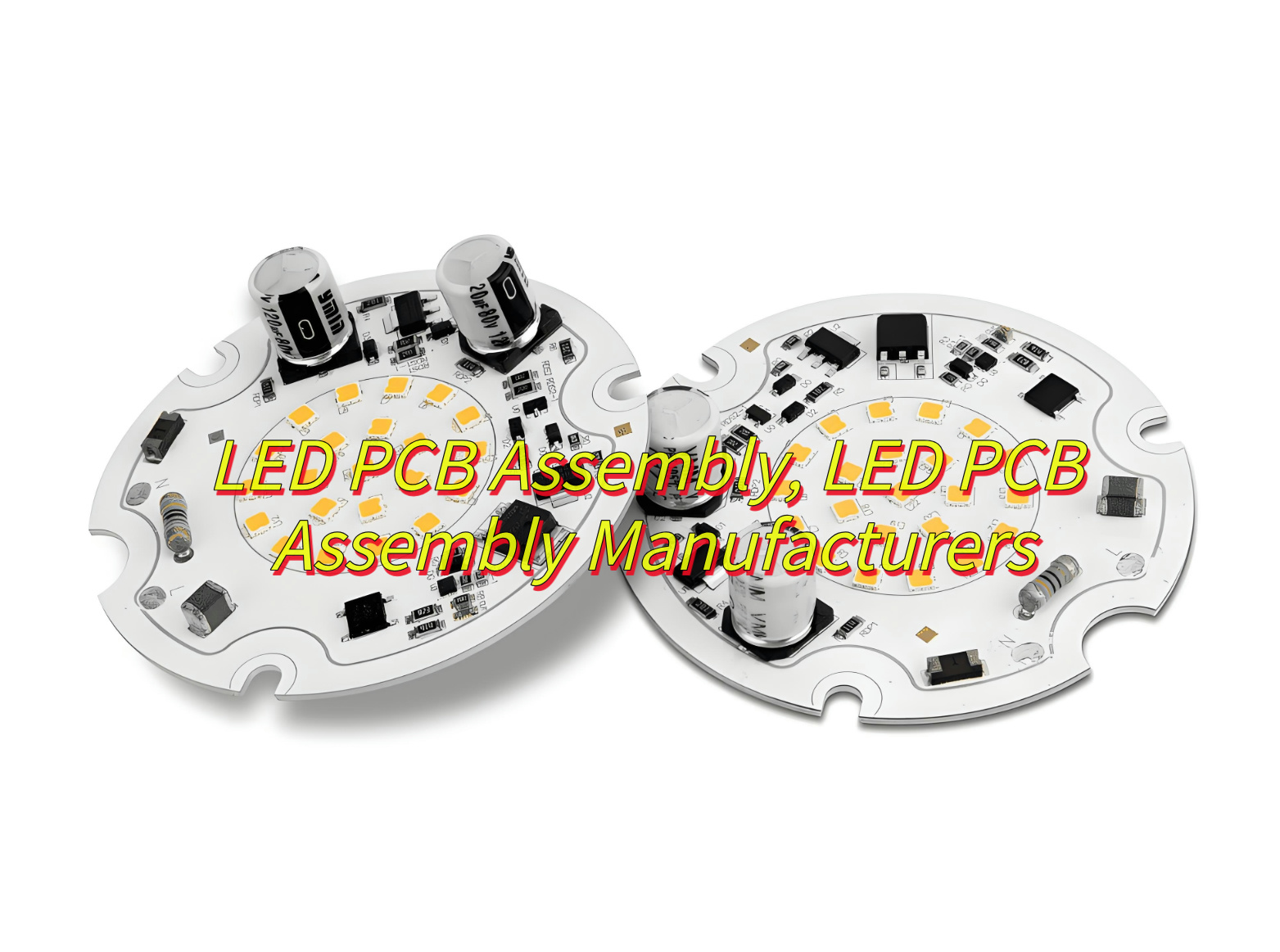
Are you find aLED PCB assembly solution? How do you find a good quality LED PCB assembly factory? This blog breaks down the essentials: assembly machines, assembly processes and cost, and how to select a reliable LED PCB manufacturer.
Best technology, we focus onLED PCB assembly over 18 years. We can achieve LED PCB fast assembly (48-72hours fast delivery) by our stable electronics supply chains and our four SMT full-automatic production lines. So we are able to ensure consistency in luminous efficiency at fast assembly. Then all the LED PCB we assembled will be full inspected before and after assembly to reduce reworking cost. If you have any request for LED PCB, please feel free to contact us. sales@bestpcbs.com
What Is LED PCB Assembly?
LED PCB assembly refers to the process of mounting LED components onto printed circuit boards (PCBs) to create functional lighting systems or electronic devices. This process combines surface-mount technology (SMT) with precision soldering to ensure reliable electrical connections. Key elements include PCB material selection (e.g., aluminum or flexible substrates), component placement accuracy, and thermal management solutions. Manufacturers specialize in this field offer end-to-end services, from design to mass production, catering to applications like LED lighting, automotive displays, and consumer electronics.
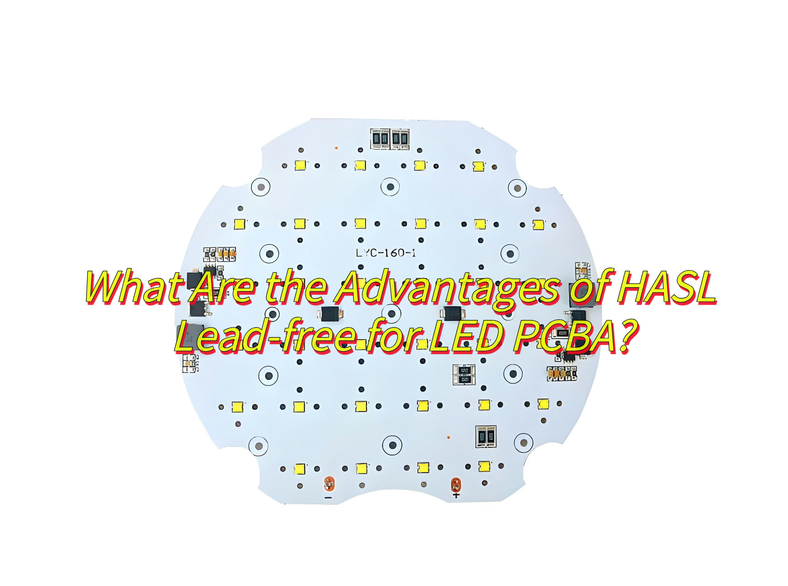
What Are the Advantages of HASL Lead-free for LED PCBA?
Environmental Compliance: Complies with the RoHS directive, eliminates lead pollution, meets global environmental regulations, and is suitable for markets with strict environmental requirements such as consumer electronics.
High Reliability: Withstands thermal cycling from -55°C to 100°C, suitable for LED applications; the tin layer prevents copper oxidation, enhancing long-term stability; good wettability in the first reflow, resulting in high soldering quality.
Significant Cost-Effectiveness: Lower cost than Electroless Nickel Immersion Gold (ENIG), suitable for medium-budget projects; mature process, suitable for mass production, reducing unit costs; long shelf life (stable for one year under moisture-proof conditions), reducing storage and rework risks.
Processing Convenience: Compatible with single/double-sided and multilayer boards (1-26 layers), meeting complex design requirements; short production cycle (12-20 days), suitable for quick delivery; solder joint defects can be repaired with hot air, reducing scrap rates.
Long-Term Technical Advantages: Mature technology, high stability, suitable for the LED industry’s needs; reliability can be enhanced by adding a nickel layer or optimizing solder paste formulations.
What Assembly Machine Is Used in the LED PCBs Assembly Process?
Pick-and-place machine
Reflow oven(Nitrogen reflow is optional, it is very stable but the cost of this kind of assembly machine is much higher than normal reflow oven)
Solder paste printer
SPI inspection machine
AOI inspection machine
X-Ray inspection machine
Conformal coating machine
Functional testing equipment
What Are 5050 LED PCB Assembly Process Steps?
Here’s a streamlined list of the 5050 LED PCB assembly process steps:
1. Incoming inspection of LED/materials
Use a two-dimensional measuring instrument and a film thickness tester to check the appearance size of the LED bracket, the thickness of the electroplating layer, and the oxidation phenomenon .
Verify the specifications of the 5050 LED (package size 5.0×5.0×1.6mm, polarity identification) and the IC model (such as SK6812) .
2. Baking materials
Unopened LEDs need to check the air tightness of the packaging, and complete the soldering within 24 hours after opening; if moisture is absorbed, it needs to be baked at 60℃ for 24 hours .
Pre-bake the PCB board (120℃/2H) to remove moisture .
3. Pick and Place &Solder paste printing
Use a laser steel mesh to print SAC305 lead-free solder paste, with a thickness control of ±10μm
Clean the steel mesh regularly to avoid clogging and uneven printing .
4. SPI Inspection
Use 3D optical detection of solder paste volume, coverage area, and offset to ensure printing quality.
5. SMT( Surface Mounted Technology)
IC (such as WS2812B) and small resistors and capacitors are mounted first, and 5050 LED is mounted last.
Check that the polarity mark (cathode/anode) is aligned with the PCB silk screen.
Certified Quality Assurance-The manufacturer holds international certifications like ISO 9001, ISO 14001, and UL, ensuring their quality management system and products meet global standards.
Advanced Technical Capabilities-They possess state-of-the-art equipment and technology, such as AOI machines and X-ray detection, enabling precise and high-quality production. They can also handle special processes like HDI boards and rigid-flex boards.
Rigorous Quality Control-A comprehensive quality control process is in place, covering incoming material inspection, in-process inspection, and final product testing. Reliability tests ensure the PCB’s stability and durability.
Flexible Production Capacity-The manufacturer can handle both small and large orders, adapting to different complexities and changes in demand, ensuring timely delivery.
Excellent Customer Service-They provide responsive communication, prompt technical support, and engineering assistance, such as DFM analysis, to help optimize your design and ensure a smooth production process.
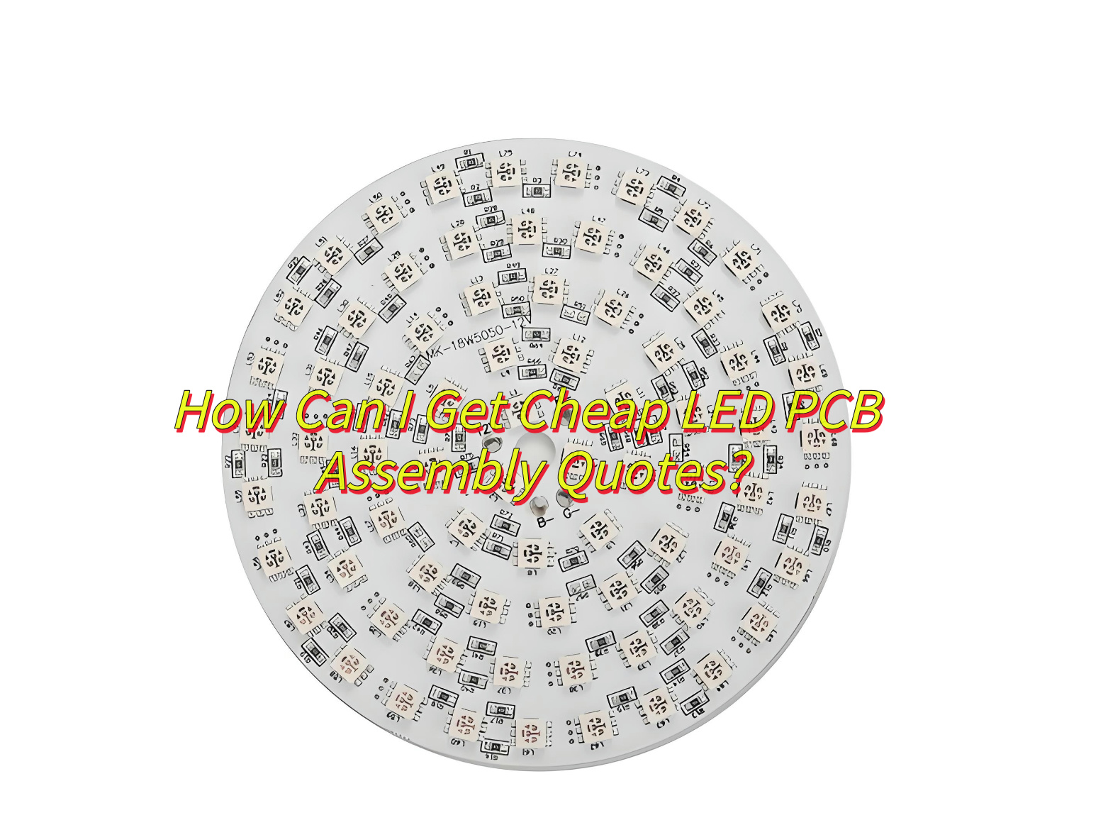
How Can I Get Cheap LED PCB Assembly Quotes?
To get cheap LED PCB assembly quotes, follow these steps:
Compare Multiple Manufacturers: Contact several manufacturers to compare prices and services.
Provide Detailed Specifications: Clearly outline your PCB requirements, including layer count, material, and components.
Optimize Your Design: Simplify your PCB design to reduce costs.
Order in Bulk: Larger orders often qualify for volume discounts.
Build Long-Term Relationships with one supplier: Negotiate better rates by committing to repeat business.
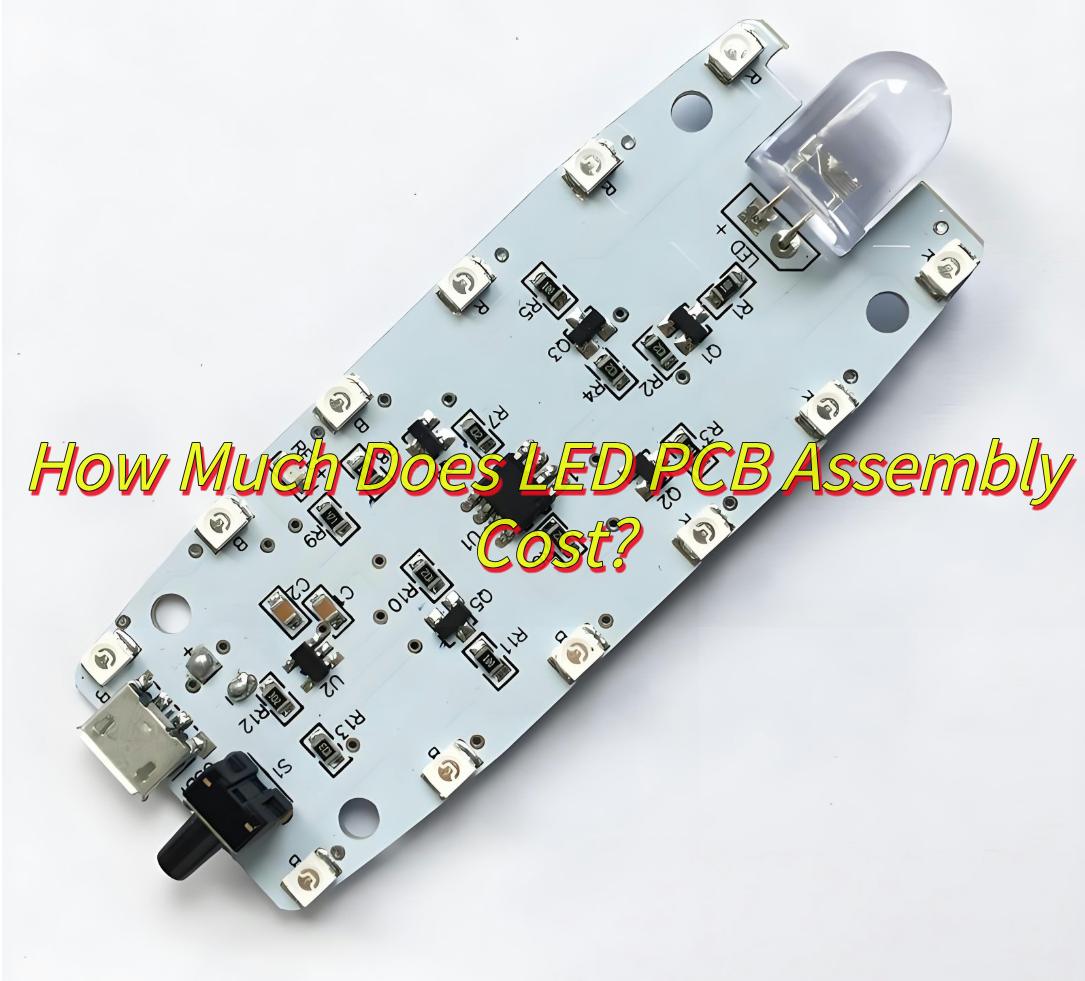
How Much Does LED PCB Assembly Cost?
Here is a LED PCB Assembly pricelist:
Setup fee: Around $200
Placement cost: Around $0.01-$0.05 per component
Standard LEDs (e.g., 5050 RGB): Around $0.10-$5 per unit
Specialty LEDs (e.g., SK6812): Around $0.50-$5 per unit
Solder Paste Stencil:Around $100
AOI Testing: Around $50-$100 per batch
Functional testing: Around $100 per batch
Conformal Coating: Around $1-$10 per board
Packaging: Around $3-$7 per unit
Note: Prices assume mid-range specifications and bulk orders. For exact quotes, please provide BOM and Gerber files with EBest Circuit (Best Technology).
What Are Differences Between Aluminum and Flex LED PCB Assembly?
Here are the main differences between Aluminum and Flex LED PCB Assembly:
Material and Structure Aluminum PCB: Uses an aluminum base for heat dissipation, suitable for high-power LEDs. Flex PCB: Made of flexible materials, allowing bending and complex shapes.
Thermal Performance Aluminum PCB: Excellent heat dissipation, ideal for high-temperature applications. Flex PCB: Limited heat dissipation, suitable for low-power applications.
Applications Aluminum PCB: Commonly used in high-power LED lighting and power modules. Flex PCB: Suitable for irregular or complex spaces, such as automotive lighting and wearables.
Cost Aluminum PCB: Generally more cost-effective for mass production. Flex PCB: Higher cost due to specialized materials and manufacturing.
Manufacturing Complexity Aluminum PCB: Simpler manufacturing process. Flex PCB: Requires specialized equipment and techniques for complex designs.
In conclusion, that’s all about LED PCB assembly and how to select a good quality LED PCB supplier. If you have any issues about LED PCB, welcome to leave a message below this blog.
Would you like to know how to DIY a keyboard LED PCB? This blog covers everything from DIY PCB layouts and RGB effects to polarity checks and troubleshooting, ensuring a seamless path from prototype to production.
EBest Circuit (Best Technology) specializes inkeyboard LED PCB solutions, deliveringstrict IP protection (NDA agreements and encrypted R&D processes), proven 8×16 RGB matrix technology (refresh rates ≥200Hz, current control within ±5%), and modular designs. Our aluminum substrates and QMK/VIA-compatible firmware ensure thermal stability and ultra-low latency (<3ms), while high-reflectivity materials reduce power consumption by 15-20%. Supported by a 24/7 multi-engineer team offering free design technical support, integrated DFM analysis, and EMC testing, we promise one-time prototyping success. If you have any request in keyboard LED PCB, please feel free to contact us: sales@bestpcbs.com
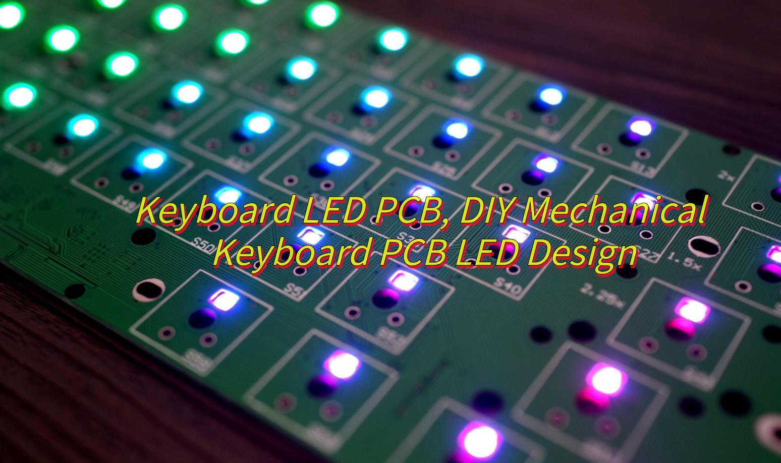
What Is A Keyboard LED PCB?
A Keyboard LED PCB is a specialized printed circuit board designed for mechanical keyboards, integrating both signal transmission and LED backlight control. Typically constructed with a metal core, such as aluminum, it efficiently dissipates heat generated by prolonged LED use while ensuring durability. Conductive copper traces on the board connect mechanical switches to LEDs, enabling real-time input signaling and customizable RGB lighting effects via embedded microcontrollers. Advanced designs may support multi-layer layouts for complex RGB configurations, software-driven light customization, and thermal management through materials like aluminum substrates.
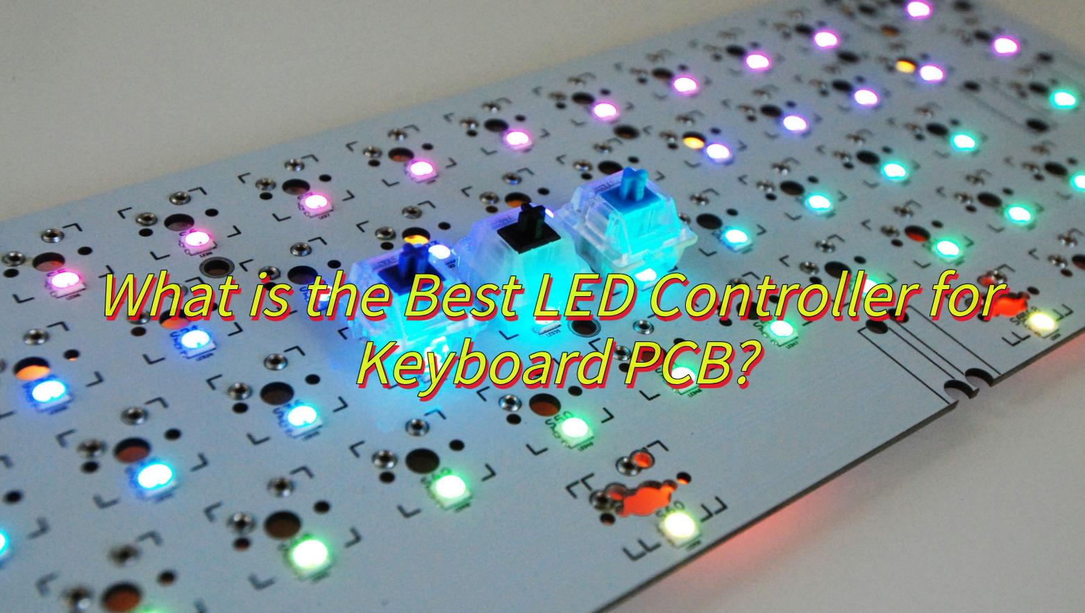
What Is the Best LED Controller for Keyboard PCB?
Compatibility: Works with your keyboard’s hardware and software.
Programmability: Supports multiple programming languages and libraries for complex effects.
Processing Power: Enough power to smoothly control multiple LEDs.
Power Efficiency: Efficient power usage to extend battery life.
Community Support: Active community for help and resources.
Switch Compatibility: Select mechanical switch type (e.g., Cherry MX) and verify footprint dimensions. Design a switch matrix (rows/columns) with N-key rollover using 1N4148 diodes. Assign rows/columns to MCU GPIO pins (e.g., ATmega32U4).
LED System: For single-color LEDs, calculate resistor values by subtracting the LED forward voltage from the power supply voltage and dividing by the desired current. For RGB LEDs (WS2812B), chain data lines (DIN→DOUT) with 0.1µF decoupling capacitors per LED and a 220Ω resistor on the data line. Ensure total LED power consumption stays below 500mA for USB compliance.
2. Power Circuit Design
Voltage Regulation: Integrate a 5V to 3.3V LDO (e.g., AP2112K-3.3V) for MCU power. Include a 10µF bulk capacitor at the USB input and 100nF decoupling capacitors near each IC.
Protection: Add a 500mA PTC fuse on the VBUS line to prevent overcurrent damage.
3. PCB Layer Stack-up and Routing
2-Layer Design: Route switch rows/columns on the top layer and dedicate the bottom layer to ground. For RGB-heavy designs, use a 4-layer stack with dedicated power/ground planes.
Signal Isolation: Route switch matrix traces perpendicular to RGB data lines to minimize interference. Keep RGB data traces under 30cm and use 0.2mm trace width with 0.1mm spacing for impedance control (~50–60Ω).
4. Thermal Management
Aluminum-Core PCB: 1.6mm aluminum substrates (e.g., Bergquist MP-06503) for high-power LED setups. Place thermal vias (0.3mm drill, 0.6mm pad) under LEDs to transfer heat to the core.
Mounting: Secure LEDs with thermal adhesive (e.g., Arctic Silver) for improved heat dissipation.
5. Component Placement
Switches: Align to a 19.05mm grid (ANSI/ISO standard). Include hot-swap sockets if required.
LEDs: Position 2.5mm below switch stems for uniform backlighting. Avoid placing LEDs near mounting screws or plate cutouts.
MCU and USB: Place the MCU close to the USB connector. Add ESD protection (e.g., USBLC6-2SC6) on the USB data lines.
6. Firmware Configuration
Matrix Mapping: Define row/column GPIO assignments in firmware. Assign the RGB data pin (e.g., RGB_DI_PIN = GP16).
LED Control: Implement libraries like Fast LED for animations. Apply gamma correction to ensure color accuracy.
7. Prototype Assembly and Testing
Fabrication: Order prototypes with ENIG finish and impedance-controlled traces. Specify 0.5oz copper for cost efficiency.
Functional Tests: Measure USB current draw at max brightness; ensure it stays below 500mA.
Thermal Validation: Use a thermal camera to check LED temperatures (<60°C under sustained use).
How to Avoid Keyboard LED Polarity Issues?
Align LED orientation with the PCB’s polarity symbols (e.g., anode/cathode markers like “+/-” labels or silkscreen arrows).
Verify PCB polarity markings using clear indicators (e.g., asymmetrical footprints or “+” labels) to prevent reversed installation.
Test LEDs before soldering by placing them loosely on the PCB and powering the board to confirm functionality.
Ensure correct wiring alignment for power (VCC), ground (GND), and data lines (DIN/DOUT) to match the LED pinout.
Use a multimeter to check continuity between LED pins and PCB pads for proper polarity alignment.
Select PCBs with reverse-protection features like polarity diodes or reverse-voltage-tolerant LEDs (e.g., WS2813).
Follow manufacturer pinout guides from datasheets to confirm LED and PCB specifications (e.g., WS2812B pin 1 = VCC).
Inspect solder joints to fix misaligned pins or accidental bridges that short-circuit connections.
Label custom PCBs with polarity symbols or color-coded silkscreen layers (e.g., red for VCC, black for GND).
Update firmware settings (e.g., QMK) to align GPIO pin configurations with the PCB’s electrical polarity.
How to Achieve RGB LED Effects on Keyboard PCB?
Here are steps to how to achieve RGB LED effects on keyboard PCB:
1. Hardware Design
Use a PCB that supports RGB LEDs (such as aluminum substrates for heat dissipation), and the pad size is suitable for 5050 LEDs (5mmx5mm).
Choose addressable RGB LEDs (such as WS2812B) or ordinary RGB LEDs with driver circuits (such as MOSFET+PWM).
Integrate a microcontroller (such as STM32F103) to manage signals and protocols (I²C/SPI).
2. Welding and Assembly
The soldering iron temperature is <350°C to solder the LED to avoid damage.
A series current limiting resistor (such as 0805 68Ω) prevents overcurrent.
3. Firmware Programming
Use Arduino or QMK to program dynamic effects such as breathing and rainbow.
Control brightness and RGB color mixing (0-255) through PWM dimming.
4. Software Configuration
Use Open RGB to customize single-key lighting effects and synchronize system themes.
Program macros or SDK to achieve dynamic responses (such as key-triggered lighting effects).
5. Test Optimization
Use a multimeter to check the circuit and AOI to detect the quality of solder joints.
Optimize code to reduce delays and ensure smooth lighting effects.
How to Choose the Best Keyboard LED PCB Design Service?
IP Protection: Ensure providers enforce strict NDAs. Like EBest Circuit (Best Technology), we have encrypted storage and physically isolated R&D environments to safeguard firmware code and LED matrix control logic.
Transparent Process: Prioritize modular designs (e.g., detachable LED driver layers) supported by real-time collaboration tools and standardized Gerber/BOM files for seamless production handoffs.
High-Density Expertise: Prioritize vendors with proven success in 8×16 RGB matrices, resolving ghosting/thermal issues, and delivering ≥200Hz refresh rates with ±5% current accuracy.
Signal & Thermal Performance: Verify PWM interference analysis in keyboard LED matrix layouts and thermal solutions (aluminum substrates, optimized copper layers) to prevent overheating.
Customization & Efficiency: Demand QMK-compatible firmware for low-latency effects (<3ms) and high-reflectivity materials (≥85%) to minimize power consumption in backlit designs.
Why is My Keyboard LED PCB Not Working?
Insufficient Power: If USB power exceeds limits (e.g., 1A for 50 LEDs), use an external power supply or reduce the number of LEDs.
Voltage Drop: Measure voltage at the LED endpoints. If below 4.5V (for 5V LEDs), thicken power traces or add external 5V power injection.
Broken Connections or Cold Solder Joints: Ensure the data line (DIN) is sequentially soldered. Re-solder loose joints.
Short Circuits: Check for accidental solder bridges or debris between pins/traces.
Incorrect Pin Mapping: Verify the GPIO pin assigned to the data line in firmware (e.g., QMK) matches the PCB design.
Missing Drivers: Install libraries like Fast LED or update MCU firmware to support LED protocols (e.g., WS2812B).
Burned LEDs/MCU: Test components individually and replace faulty ones.
Broken PCB Traces: Check for broken traces in high-current areas (e.g., power lines) with a multimeter.
Can You Build a Keyboard LED Only PCB?
Yes, you can build a keyboard PCB solely for LEDs, but it requires designing a dedicated circuit for power delivery and control signals. Focus on high-current traces (≥1A) to handle multiple LEDs, integrate voltage regulation (3.3V/5V), and support addressable protocols (e.g., WS2812B) with proper data-line routing. Ensure physical spacing avoids interference between LEDs and omit switch footprints. Pair it with a compatible controller (e.g., RP2040) for firmware-driven effects. This setup suits decorative lighting or auxiliary backlighting but lacks switch functionality.
Are you interested in power LED PCB and how to design a high power LED PCB board? Let’s learn more about types, advantages of power LED PCB and how to design high power LED PCB for better dissipation through this blog.
EBest Circuit (Best Technology), we focus onpower LED PCBdesign service over 18 years. And we deliver high-performance Power LED PCBs with free technical support, multi-engineer collaboration, and cost-saving DFM analysis to optimize designs and reduce production cost. Rigorous in-house EMC testing ensures compliance (FCC/CE), while rapid prototyping (<7 days) and ISO 9001/RoHS/UL-certified manufacturing guarantee reliability. Leverage our expertise in thermal management, custom substrates (aluminum/ceramic), and eco-friendly practices to cut costs and accelerate your project. If you have any request for power LED PCB, please contact us: sales@bestpcbs.com
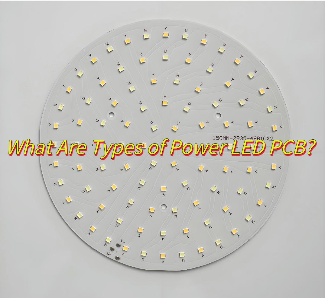
What Is Power LED PCB?
Power LED PCB is a printed circuit board designed for high power LEDs.(like high power 3535 LED PCB and high power 5050 LED PCB). It uses a metal substrate (such as aluminum) and a special thermal conductive structure to achieve efficient heat dissipation. It ensures stable transmission of large currents by widening copper foil routing and optimizing pad layout. It is widely used in high-intensity solid-state lighting systems such as industrial lighting and car lights.
What Are Types of Power LED PCB?
Types of Power LED PCBs:
Metal-Core PCB (MCPCB)-Aluminum or copper substrates with insulated thermal layers for high-power LED lighting such as streetlights and automotive headlights, like power LED aluminum PCB.
Heavy Copper PCB-Thick copper traces (≥3 oz/ft²) for high-current applications like LED driver circuits and industrial power modules.
Multi-Layer PCB-4+ conductive layers with thermal vias and EMI shielding for LED displays, automotive electronics.
High-Frequency PCB-Low-loss materials (e.g., PTFE) for stable signal transmission in 5G/RF lighting and radar systems.
Rigid-Flex PCB-Hybrid design combining rigid stability and flexible routing for automotive lighting.
What Are Advantages of LED Power PCB?
Advantages of LED Power PCBs:
Efficient thermal management ensures optimal heat dissipation, prolonging LED lifespan.
High energy efficiency with minimal power loss due to low-resistance circuitry.
Compact design enables integration into space-constrained applications.
Enhanced durability with robust materials resistant to vibration, moisture, and temperature fluctuations.
Precise current regulation improves LED performance and brightness consistency.
Eco-friendly operation with low power consumption and reduced carbon footprint.
Customizable layouts support complex circuit designs for diverse LED applications.
Cost-effective production through scalable manufacturing and reduced maintenance needs.
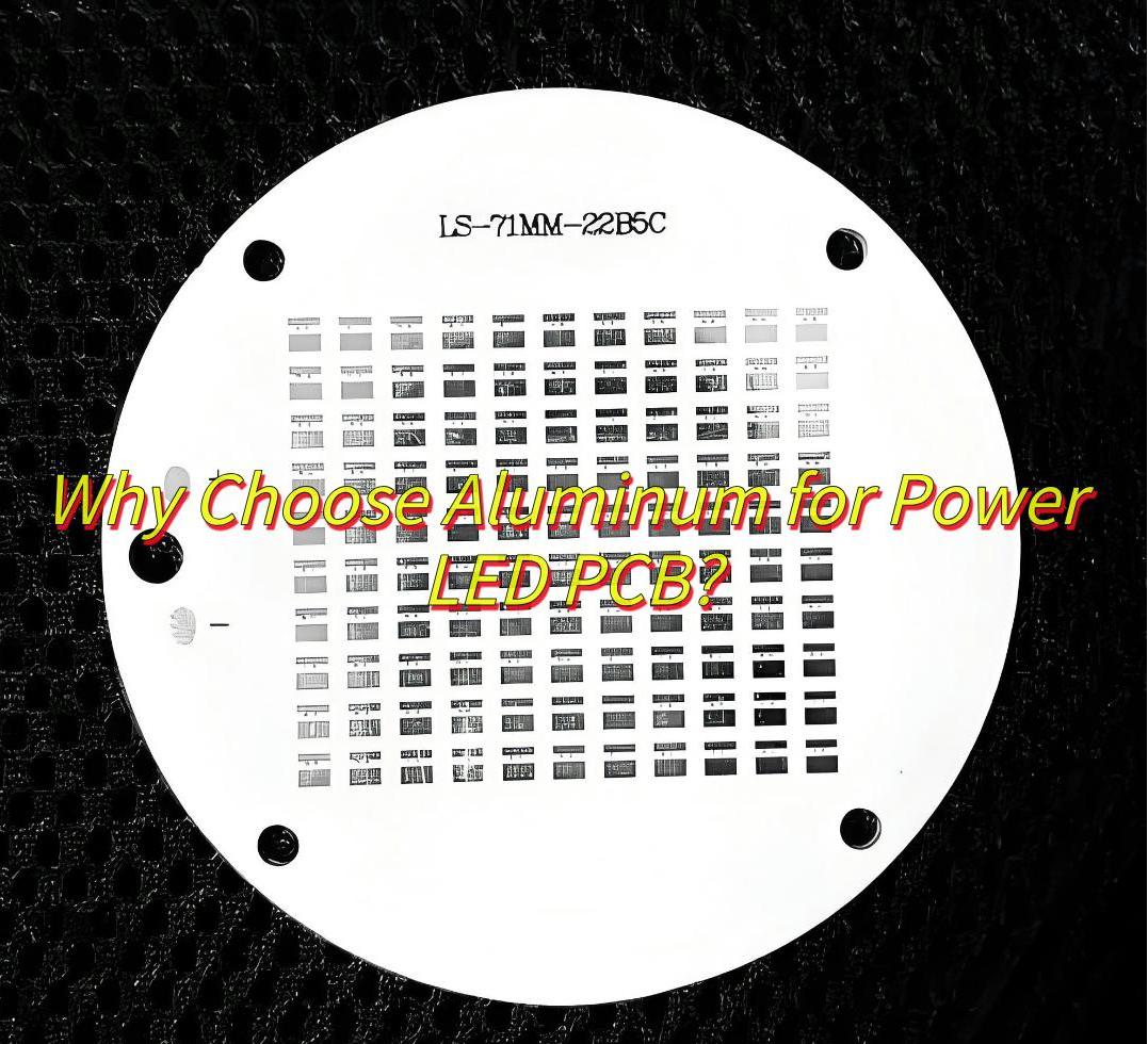
Why Choose Aluminum for Power LED PCB?
Reasons for why choose aluminum for power LED:
Efficient Heat Dissipation: High thermal conductivity prevents overheating, extending LED lifespan.
Durability: Resists thermal stress, vibration, and maintains precise dimensions.
Electrical Reliability: Handles higher currents, blocks interference, and ensures insulation.
Cost-Saving: Recyclable material, reduces heatsink needs, and lowers bulk production costs.
Custom Design: Adapts to complex shapes and multi-color LED configurations.
Use 2oz copper thickness for power traces and widen ground planes to reduce resistance.
4.Thermal Management Execution
Drill thermal vias (0.4mm diameter) under LED pads, filled with conductive epoxy (≥4 W/mK).
Attach extruded aluminum heatsink (30×30×15mm) using thermal tape (3.5 W/mK).
5.Optical Enhancement
Apply 98% reflective white solder mask around LEDs and use 45° angled sidewalls to maximize light output.
Embed diffuser layer (PC material) in the final assembly to homogenize brightness.
6.Prototyping & Testing
Measure luminous flux with integrating sphere, calibrate PWM duty cycle to achieve ±3% brightness uniformity.
7. EMI/EMC Compliance
Add π-type filters (10µF ceramic + 10µH inductor) at driver input/output to suppress noise.
Test radiated emissions per FCC Part 15B using near-field probes.
8.Production Readiness
Generate Gerber files with 0.2mm solder mask dam and 0.15mm solder paste stencil.
Validate assembly process with 3D STEP model to check component clearance.
How to Balance Current in High Power LED PCB Layouts?
To balance current in high power LED PCB layouts:
Symmetrical Star-Shaped Routing
Arrange LEDs in a radial pattern with equal-length traces radiating from a central power node. This minimizes impedance differences between parallel branches, ensuring even current distribution.
Use identical trace widths and spacing for all parallel paths to eliminate resistance variations.
Thick Copper Layers (≥3 oz/ft²)
Increase copper thickness to reduce resistive losses in high-current paths. For example, 3 oz/ft² copper handles up to 6A/mm trace width (vs. 3A/mm for 1 oz/ft²).
Prioritize short, direct traces to minimize voltage drops.
Thermal Symmetry
Align PCB thermal management structures (e.g., heat sinks, thermal vias) symmetrically around LEDs to maintain uniform junction temperatures.
Avoid placing high-power components near PCB edges, which can create thermal gradients.
Parameter Matching
Use LEDs from the same production batch to minimize forward voltage and current tolerance variations (ideally <2% mismatch).
Group LEDs with similar electrical characteristics into parallel clusters.
Low-Impedance Grounding
Design a solid ground plane beneath power traces to stabilize return paths and reduce EMI-induced current fluctuations.
Place decoupling capacitors near LED nodes to suppress transient noise.
Active Current Regulation
Integrate current-sharing resistors (e.g., 0.1Ω–0.5Ω) in series with each LED branch to compensate for minor mismatches.
For precision control, use dedicated LED driver ICs with built-in current balancing (e.g., TLC5916, LT3763).
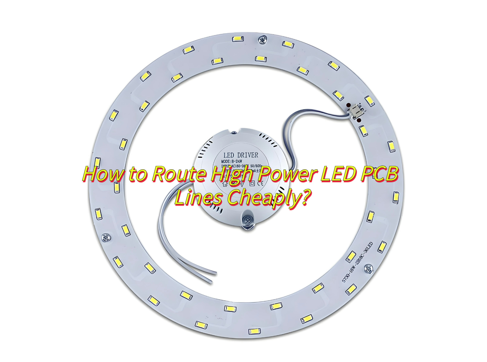
How to Route High Power LED PCB Lines Cheaply?
To route high power LED PCB lines cheaply:
Prioritize single/double-layer PCB designs with 2oz copper thickness for current capacity, using FR4 substrates instead of metal-core boards. Integrate 12–24 thermal vias (0.3mm diameter) per LED and attach extruded aluminum heatsinks (cost ≤$0.10/cm²) for thermal management.
Follow the 3W spacing rule: Maintain ≥3× trace width between conductors (e.g., 0.6mm spacing for 0.2mm traces) to reduce interference. Add 1mm isolation zones for critical signals like clocks or high-speed lines.
Cluster components (LEDs, drivers, capacitors) within 15mm radius: Use star topology for power routing (<30mm trace length) and implement solid ground planes with multi-point connections (impedance below 5mΩ).
Match trace widths to current loads using PCB current calculators. Use tapered traces to minimize current spikes and avoid excessive temperature rise.
Simplify driver circuits: Use linear ICs (e.g., AMC7135) with 1% current-limiting resistors for <2A applications. For >2A, adopt discrete MOSFET solutions to cut costs by 40% compared to integrated ICs.
Can Multi-Layer Designs Solve High Power LED PCB Overheating?
Yes, multi-layer design can effectively alleviate the overheating issue of high power LED PCBs. By embedding a thick copper layer (≥2 oz) as a heat dissipation layer and combining vertical thermal vias (0.3–0.5mm) to quickly guide heat to the radiator, the symmetrical stacking structure and high temperature substrate (such as aluminum baseboard) can disperse thermal stress. In conjunction with active cooling measures (such as thermal interface materials), it is possible to control the junction temperature within a safe range (<85°C). However, it is necessary to plan the thermal path and electrical isolation reasonably to avoid thermal coupling failure.
In conclusion, that’s all about power LED PCB and how to design a high power LED PCB board for better dissipation. If you have any other issues for power LED PCB and high power LED PCB, welcome to leave a message below this blog.
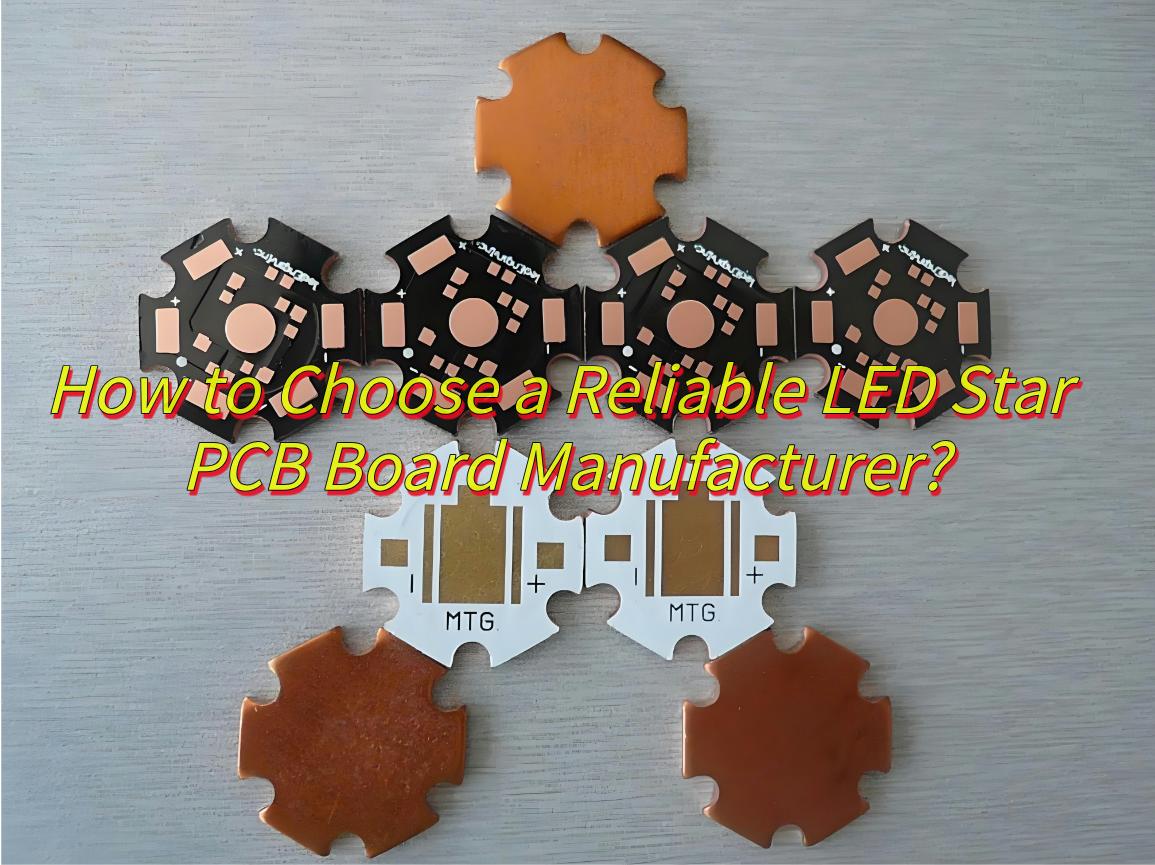
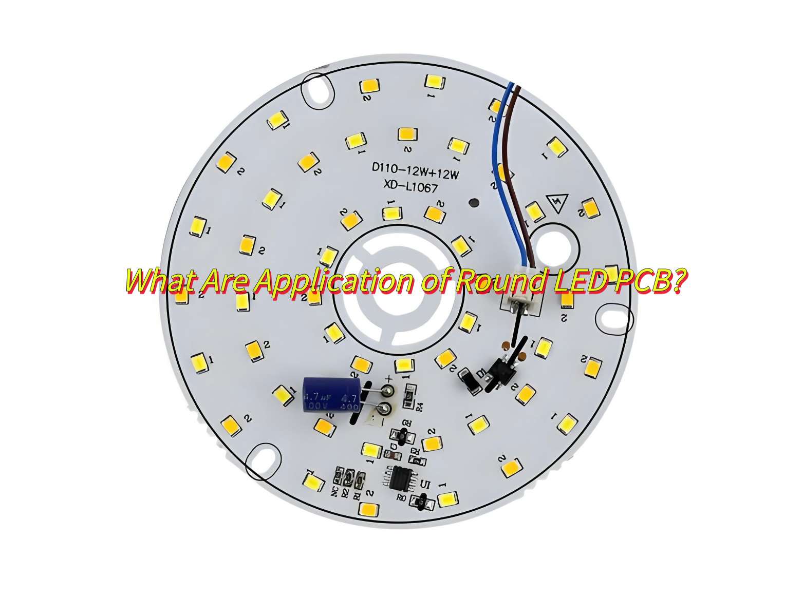
Are you looking for a competitive LED Star PCB manufacturer? Let’s explore more about LED star PCB’s advantage and application as well as how to select a trusted LED star PCB board manufacturer.
As a trusted LED Star PCBmanufacturerwith full ISO/UL/CE certifications, EBest Circuit (Best Technology) have scalable SMT production lines, and rigorous IQC-FQC quality protocols validated through thermal/vibration/aging tests. Our vertically integrated supply chain ensures flexible MOQs with affordable price, stable lead times, and end-to-end logistics support from compliant export packaging to freight optimization. And we also support customized LED star PCB, such as material, dimension and color customization. If you have any request for LED star PCBs, please contact us: sales@bestpcbs.com
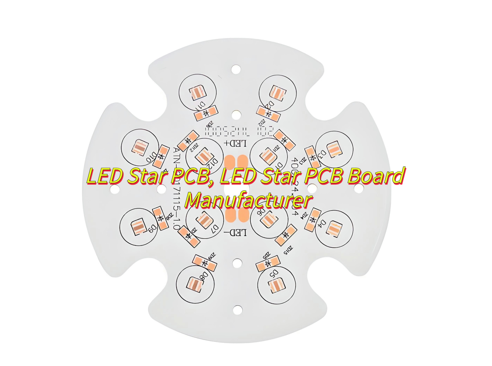
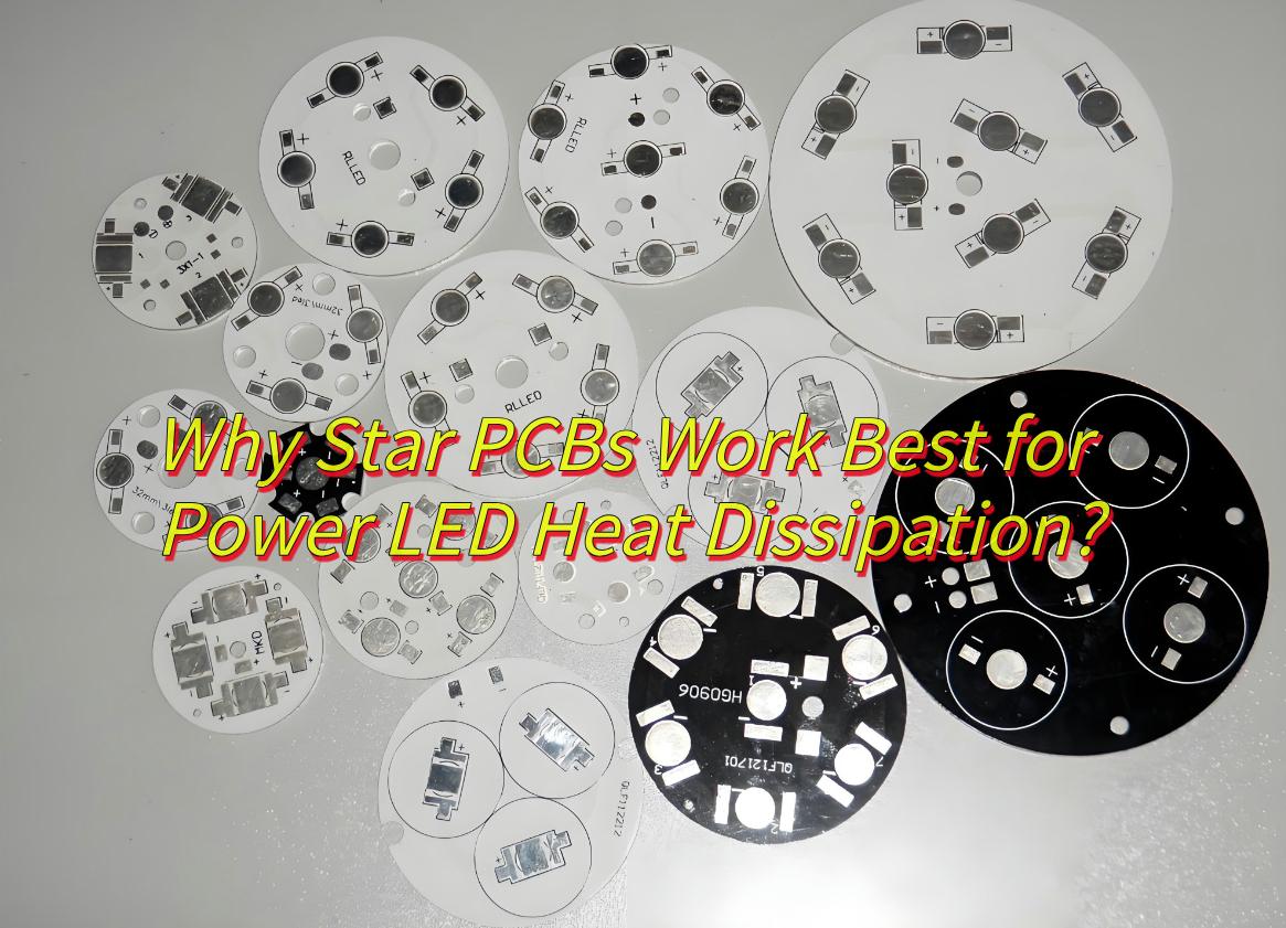
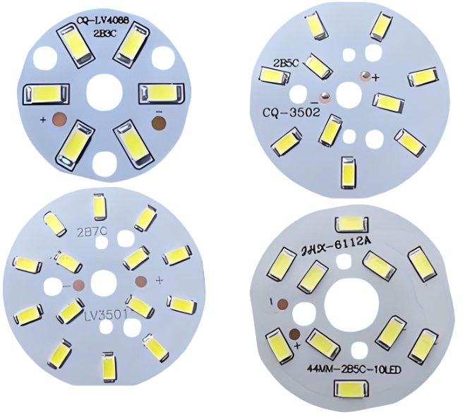
What Is LED Star PCB?
LED Star PCBis a specialized printed circuit board designed for high-density LED installations, featuring a star-shaped layout that optimizes thermal management and light distribution. This configuration allows multiple LEDs to be arranged in a radial pattern, enhancing heat dissipation through increased surface area and airflow efficiency. The board typically incorporates advanced materials like aluminum or ceramic substrates to further improve thermal conductivity, making it ideal for high-power LED applications. Its modular design enables flexible customization in terms of LED quantity, color (including red LED star PCB and other RGB LED star PCB options), and dimensions, catering to diverse lighting needs such as decorative lighting, stage effects, and industrial illumination.
Verify Core Competencies – Check ISO/UL/CE certifications, factory scale, and SMT line capacity to ensure quality standards and production capability
Evaluate Quality Systems – Assess IQC/IPQC/FQC processes and request sample testing (thermal cycling, vibration, aging) to validate reliability
Analyze Supply Chain – Investigate component sourcing, MOQ policies, and lead times to ensure stable production and timely delivery
Review Customization Track Record – Examine case studies of similar projects and R&D team expertise to confirm design flexibility
Compare Total Cost Structure – Analyze pricing transparency, material specifications, and hidden costs while balancing MOQ requirements
Assess Logistics & Support – Confirm export packaging compliance, freight partnerships, and after-sales policies (warranty/technical support)
Evaluate Long-Term Viability – Investigate financial stability, cultural alignment, and sustainability practices for sustainable partnerships
Check Risk Mitigation – Verify crisis response plans, insurance coverage, and alternative supply options to ensure business continuity
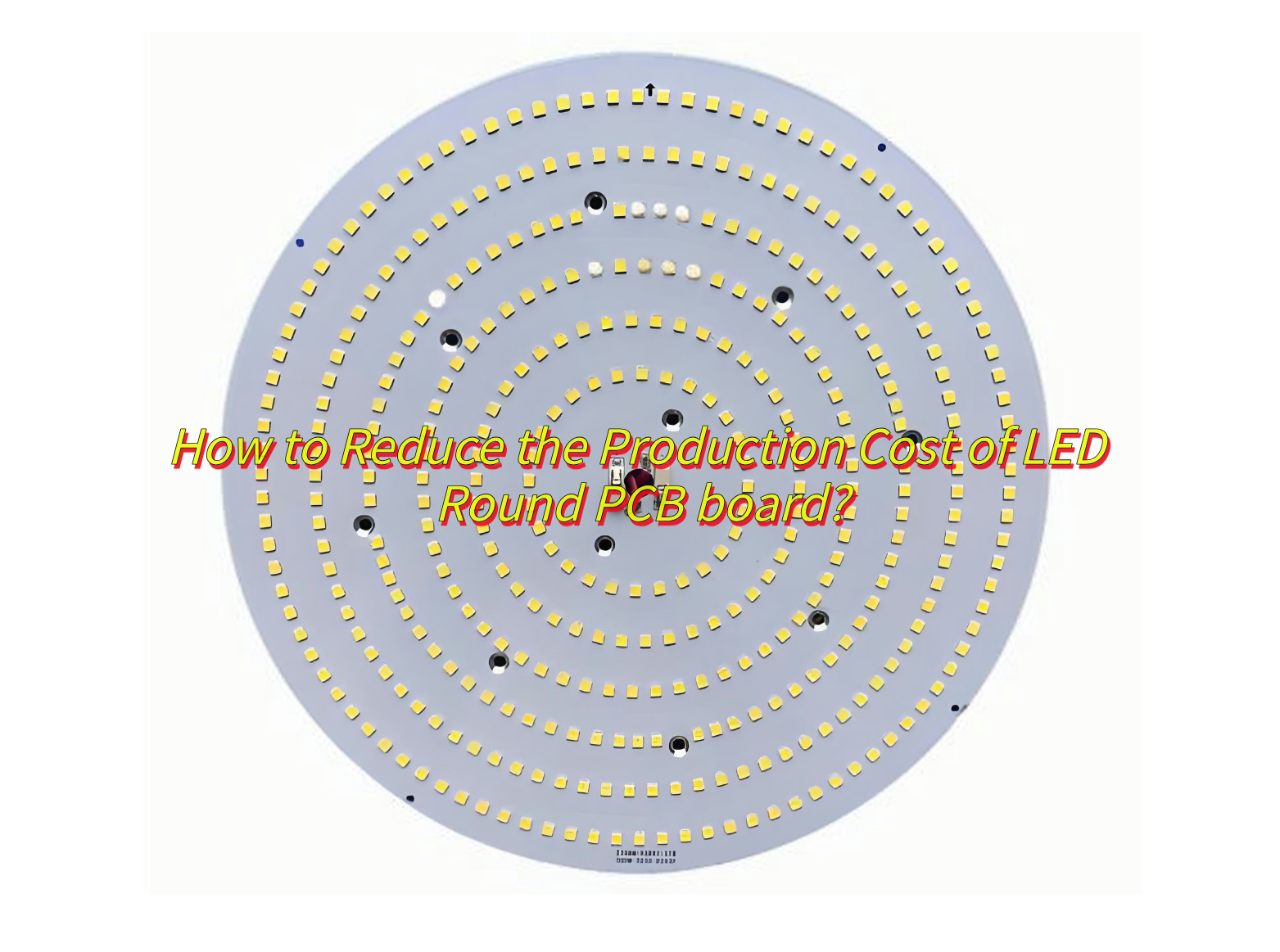
How to Reduce the Production Cost of LED Star PCB?
Here are some methods about how to reduce the production cost of Star LED PCB:
Standardize Component Specifications-Unify LED packaging formats to minimize redundant layers and blind/buried via designs, reducing material waste and processing complexity.
Cost-Effective Material Selection-Adopt high-performance FR4 substrates while optimizing copper foil thickness to balance thermal/electrical performance with material cost reliability.
Streamlined Manufacturing Process-Utilize DFM (Design for Manufacturing) tools to validate layouts, eliminating precision alignment requirements and complex solder mask processes for improved yields and reduced costs.
Automated Production & Stencil Optimization-Implement automated placement equipment to lower labor costs, paired with optimized stencil apertures that minimize solder paste waste.
Centralized Procurement & Supplier Collaboration-Partner with manufacturers supporting small-batch prototyping and mass production, leveraging long-term agreements or BOM substitution strategies to reduce component expenses.
Early-Stage Design Validation-Require suppliers to provide thermal distribution and signal integrity simulation reports to prevent costly rework in later stages.
Modular Design for Maintainability-Implement replaceable sub-modules to reduce repair costs and extend product lifecycles.
Dynamic Dimming Algorithm & Driver IC Optimization-Reduce LED counts or adopt cost-effective driver ICs, combining PWM compensation strategies to maintain performance-cost balance.
How to Achieve Multi-color Synchronous Control with RGB LED star PCB?
To achieve multi-color synchronous control with RGB LED star PCB:
Use I2C driver chips (e.g., IS31FL3236A) combined with STM32F103 MCU, supporting 36-channel PWM control to achieve 256-level brightness mixing for 12 groups of RGB LED star PCBs.
Wired synchronization: Cascade driver chips via I2C/SPI buses with timing synchronization error <1μs; Wireless synchronization: ESP32-C3 Mesh network synchronizes 100+ nodes with transmission delay <5ms.
HSV-CIE1931 color space conversion algorithm ensures multi-board color difference <±3%; DMA-driven real-time PWM duty cycle updates eliminate cascaded brightness deviations.
Symmetrical star-shaped wiring design: ±2mm wire length difference between LEDs and MCU to reduce phase mismatch; Layered stack structure (thickness ≤1.6mm) integrates LED arrays on top layer and driver circuits on the bottom.
Yes, LED Star PCB dimensions can be fully customized (e.g., diameter 50-200mm). EBest Circuit (Best Technology) also supports color customization through RGB channel configuration, driver chip selection, and dynamic dimming algorithms. Material customization, size adjustments and color control (including multi-color synchronization) are tailored to meet specific application requirements, such as stage lighting or automotive ambient systems. If you want to get a quote for customized LED star PCB, please feel free to leave a message below this blog.
A 2W SMD LED light PCB is a type of circuit board designed to incorporate SMD LEDs mounted directly onto the board. The 2W designation refers to the thermal conductivity of the dielectric layer of the PCB, which typically uses aluminum to provide superior heat dissipation. The high thermal conductivity ensures that the LEDs operate efficiently even under high power, as it minimizes heat buildup—an essential factor for maintaining the longevity and performance of the LEDs.
This type of PCB is highly effective for applications where efficient cooling and energy-saving properties are needed, such as downlights, track lighting, spotlights, and even automotive lighting. The aluminum base serves a dual purpose: providing robust mechanical support and facilitating effective heat management.
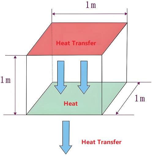
What is Thermal Conductivity of a LED light PCB?
Thermal conductivity refers to the ability of a material to conduct heat. It is defined as the amount of heat transferred through a 1-meter thick material with a temperature difference of 1 degree (K or °C) across its surfaces under steady-state conditions. This heat transfer per second through a 1-square meter area is measured in watts per meter per degree (W/(m·K)), where K can be replaced by °C. Thermal conductivity applies specifically to heat transfer by conduction. When other forms of heat transfer, such as radiation, convection, and mass transfer, are present, the combined heat transfer relationship is often referred to as theapparent thermal conductivity, effective thermal conductivity, or thermal transmissivity of the material.
In addition, thermal conductivity is defined for homogeneous materials. In practice, materials may be porous, layered, have multiple structures, or be anisotropic, and the thermal conductivity of such materials represents an overall composite thermal performance, often referred to as the average thermal conductivity.
The thermal conductivity of an LED light PCB is typically determined by the material used in the dielectric layer of the PCB. Common materials for LED PCBs include aluminum and copper, which have high thermal conductivity, allowing them to efficiently dissipate heat.
Thermal Conductivity and its Impact on LED Light PCB
For LED light PCBs, effective heat dissipation is critical for maintaining brightness, efficiency, and longevity. If the thermal conductivity is insufficient, the LED may overheat, causing:
Reduced light output: Overheating can cause LEDs to dim or malfunction.
Shortened lifespan: Excessive heat can lead to the degradation of LED components, reducing their operational life.
Instability: Poor heat management can lead to thermal runaway, where the heat generated causes even more heat to accumulate, damaging the LED permanently.
Aluminum 2W SMD LED Light PCB Specification
Product Name
2W SMD LED Light PCB
Base Material
Aluminum
Layer Count
2L (Double Sided)
Board Thickness
1.6mm +/-10%
Dielectric Thermal Conductivity
2W
Copper Thickness
1OZ
Solder Mask
Black
Silkscreen
White
Surface Finishing
HASL Lead-Free
Hole Tolerance
PTH: ±0.075; NTPH: ±0.05
Shape
Square
Assembly
NO
Ship by Panel or Single Piece
Single Pieces
Benefits of 2W LED Light PCB
1. Efficient Heat Dissipation
One of the standout features of the 2W LED light PCB is its 2W thermal conductivity, which allows for superior heat dissipation. So that the aluminum base can transfer heat away from the LED, ensuring that the light source remains cool. By keeping the LED cool, the PCB extends the overall lifespan of the lighting system.
2. Energy Efficiency
While the 2W LED light PCB offers excellent heat management, it also delivers superior energy efficiency. With reduced power consumption compared to traditional lighting options, it offers a bright light output while keeping energy costs low.
3. Compact and Lightweight Design
The aluminum light PCB is typically smaller and lighter than many other types of lighting solutions, such as copper core LED PCB or sinkpad LED PCB. Whether it’s downlights, track lights, or under-cabinet lighting, the small form factor of the 2W LED PCB allows for easy installation in tight spaces.
4. Long Lifespan
Thanks to the efficient thermal conductivity and the energy-efficient design, 2W LED light PCBs have a much longer lifespan compared to traditional lighting options. While conventional bulbs often burn out or degrade quickly, LEDs can last for tens of thousands of hours.
5. Environmentally Friendly
Aluminum LEDs are known for being environmentally friendly. These lights consume far less energy than traditional incandescent or halogen bulbs, resulting in lower carbon emissions. Additionally, LEDs contain no harmful chemicals like mercury, which makes them easier to recycle compared to other lighting technologies.
6. High Color Rendering Index (CRI)
Many 2W LED light PCBs offer a high Color Rendering Index (CRI), which means they provide better color accuracy in the light they produce. This is particularly important in areas where accurate color display is crucial, such as in retail settings, art galleries, or photography studios.
1W vs. 2W vs. 3W LED PCB
When designing a LED PCB, it is important to choose a suitable thermal conductivity to ensure an effective heating dissipation. In EBest Circuit (Best Technology), we offer 1W, 2W and 3W LED PCB. Though the higher thermal conductivity means better heat dissipation, but not higher is best for your devices. Let’s see what are the differences between them and how to choose them.
Feature
1W LED PCB
2W LED PCB
3W LED PCB
Thermal Conductivity
1.0 W/m·K
2.0 W/m·K
3.0 W/m·K
Heat Dissipation
Good heat dissipation, suitable for low-power LEDs
Better heat dissipation than 1W, suitable for medium-power LEDs
Excellent heat dissipation, suitable for high-power LEDs
Power Consumption
Typically around 0.5W to 1W
Typically around 1W to 2W
Typically around 2W to 3W
Applications
Small indicators, backlighting, decorative lighting
When sourcing aluminum LED light PCBs, do not miss out EBest Circuit (Best Technology)! We are a China based metal core PCB manufacturer, who has engaging in PCB manufacturing for over 18 years. We specialize in a wide range of PCB types, including:
FR-4 PCB
High TG FR-4 PCB
Heavy Copper PCB
Impedance Control PCB
High-Frequency PCB
Flexible PCB
Rigid-Flex PCB
HDI PCB
Aluminum PCB
Copper-Based PCB
Ceramic PCB
And as a one-stop service to customers, we offer PCB assembly service as well, such as:
SMT (Surface-Mount Technology)
DIP (Dual In-line Package)
Reflow Soldering
Wave Soldering
Hand Soldering
Mixed Assembly Technologies
Cable Assembly
PCBA Testing
Box Building Assembly
Detail Aluminum/Copper LED PCB Manufacturing Capabilities
Aluminum/Copper LED PCB Manufacturing Capabilities By EBest Circuit (Best Technology)
LED PCB Prototype Lead Time
Prototype(<1m²)
Layers
Normal Service
Expedited Service
Metal Core PCB
1 Layer
1 – 1.5 weeks
48 hours
2 Layers
2.5 – 3 weeks
168 hours
4 Layers
3 – 4 weeks
1.5 weeks
6 Layers
4 – 5 weeks
2 weeks
8 Layers
5 – 6 weeks
TBD
10 Layers
6 – 7 weeks
TBD
LED PCB Prototype Lead Time
LED PCB Mass Production Lead Time
Mass Production
Layers
Normal Service
Expedited Service
Metal Core PCB
1 Layer
2 – 2.5 weeks
1 week
2 Layers
3 – 4 weeks
1.5 – 2 weeks
4 Layers
4 – 5 weeks
2 weeks
6 Layers
5 – 6 weeks
2.5 weeks
8 Layers
6 – 7 weeks
3 – 4 weeks
10 Layers
7 – 8 weeks
TBD
LED PCB Mass Production Lead Time
FAQs
Q1. Can you source components for my PCB?
A: Yes, we can assist in sourcing components for your PCB. We work with original manufacturers and reliable suppliers to ensure that the components meet your quality standards. We also offer BOM checking and full supply chain management to ensure timely and accurate delivery.
Q2. Can you help with PCB design and development?
A: Our team of experienced engineers can assist with both hardware and software development, including schematic design, PCB layout, and software development for embedded systems. We also offer PCBA cloning services, helping you replicate and improve existing designs.
Q3. What information do I need to get a PCB quotation?
A: Gerber file or DXF file along with your specific technical requirements, including: PCB material, thickness, copper surface specifications, solder mask and silkscreen color and any other relevant details you may have. PCB requires assembly need pick and place file and BOM file.
Q4: Are my files safe? NDA available?
A: Yes, your files are kept secure and confidential throughout the entire process. We take the protection of your intellectual property seriously and never share any customer documents with third parties. If you want to get more security, we can sign NDA file with you.
Q5. What is your minimum order quantity (MOQ)?
A: We do not have a minimum order quantity (no MOQ). Whether it’s 1pcs or 100K pcs, we are equipped to handle orders of any size flexibly.
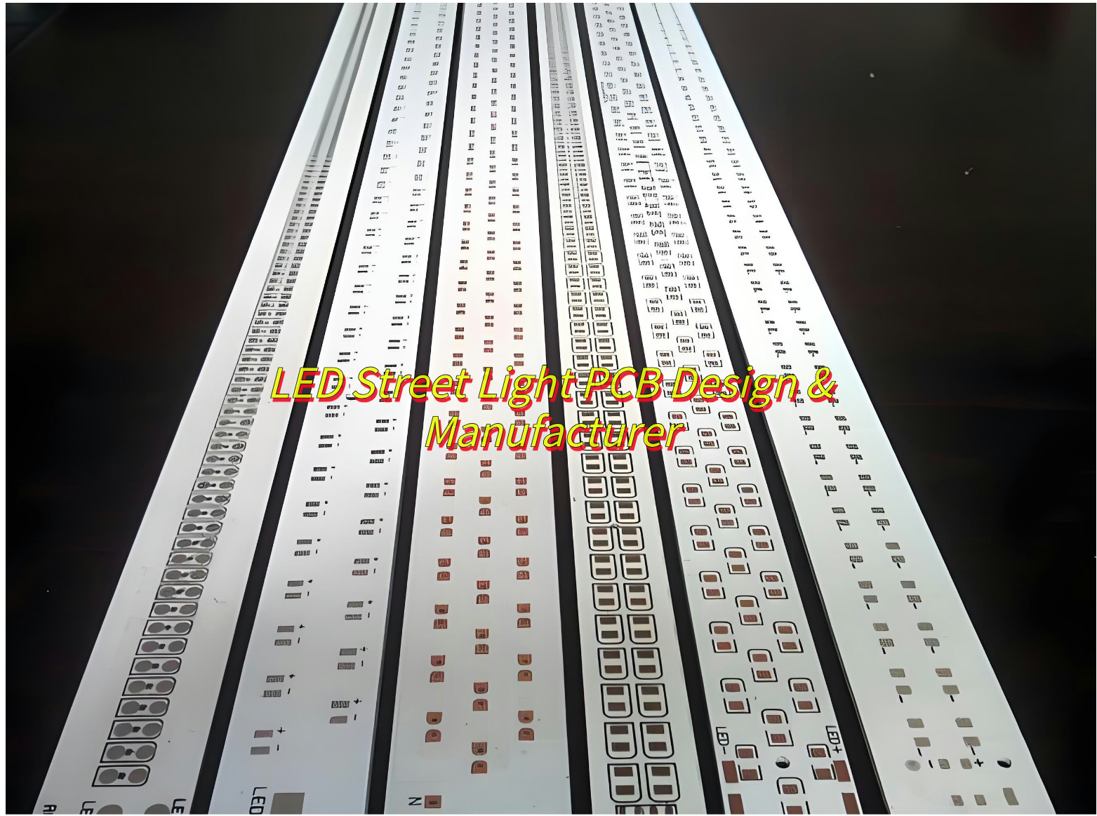
Are you looking for a LED street light PCB manufacturer with design service? Let’s learn more about advantages, design processes of LED street light PCB, and how to design it for better heat dissipation and lower cost, as well as how to select a good LED PCB supplier.
EBest Circuit (Best Technology) specialize in LED street light PCB design and manufacturing over 18 years. We use a fully automated SMT production line and AOI/X-ray inspection system, and has imported YAMAHA patch machines to ensure that the LED street light PCB patch accuracy can reach ±0.035mm, and the mounting speed can reach 95,000 points/h. Based on the 30W+ high-power heat dissipation requirements, the design end can customize the 2oz copper substrate stack and honeycomb thermal conductive hole structure, and the measured full-load temperature rise is controlled within 12°C. Passed -40°C~85°C batch-level cycle test and RoHS compliance certification, the light decay rate is ≤2.8% for 1,000 hours. Supports 15-day standard delivery and 7-day expedited delivery. If you have any request for LED Street Light PCB, please feel free to contact us: sales@bestpcbs.com
What Is LED Street Light PCB?
LED street light PCB (Printed Circuit Board) is a specialized circuit board designed to power and control LED arrays in outdoor lighting systems. Unlike conventional PCBs, these boards are engineered to endure harsh environmental conditions, including extreme temperatures, humidity, and vibration. They integrate LEDs, drivers, thermal management components, and smart sensors into a single robust platform, ensuring stable operation over decades.
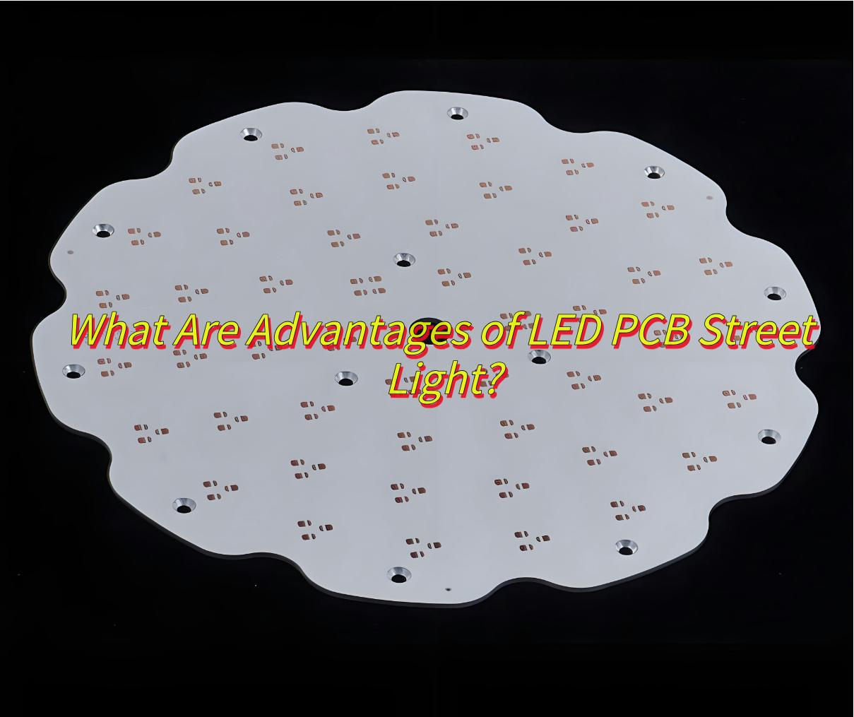
What Are Advantages of LED PCB Street Light?
LED street light PCBs offer multiple technical advantages:
Enhanced Thermal Management – Aluminum-based structures with thermally conductive dielectric layers efficiently dissipate heat, preventing overheating and extending component lifespan.
Electrical Insulation – The dielectric layer isolates circuitry from the aluminum substrate, ensuring operational safety.
High-Density LED Layout – Flexible PCB designs enable dense LED arrangements for uniform illumination without visible light spots.
Durability in Harsh Environments – Heat-resistant materials and robust construction adapt to outdoor temperature fluctuations and mechanical stress.
Energy Efficiency – Low-voltage operation and optimized thermal design reduce power consumption while maintaining brightness.
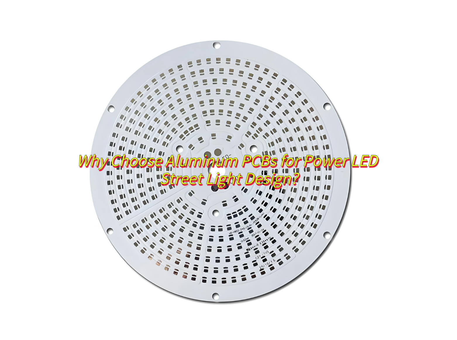
Why Choose Aluminum PCBs for Power LED Street Light Design?
Aluminum PCBs are ideal for power LED street light design due to:
Superior Heat Dissipation – Aluminum substrates rapidly transfer heat from LEDs, preventing thermal degradation and ensuring stable performance.
High Thermal Conductivity – Direct heat transfer via the metal core minimizes hotspots, critical for high-power LED longevity.
Mechanical Durability – Resists warping, vibrations, and corrosion, maintaining structural integrity in extreme outdoor conditions.
Electrical Isolation – Integrated dielectric layers prevent short circuits while enabling efficient thermal transfer.
Lightweight & Compact – Simplifies fixture design and installation without compromising heat management.
Cost-Effective Lifespan – Reduces maintenance and replacement costs by extending LED and driver life.
How to Design LED Street Light PCBs for Better Heat Dissipation?
To design LED street light PCBs for optimal heat dissipation:
1. Material Selection
Use aluminum substrates (e.g., 6063-T5 alloy) with ≥2.0 W/m·K thermal conductivity for direct heat transfer.
Prioritize 2oz+ copper layers for high-current traces to minimize resistive heating.
2. Layout Optimization
Cluster high-power LEDs centrally with ≥5mm spacing between COB modules to prevent thermal overlap.
Route traces with 4-6mm width for 3A+ currents and avoid right-angle bends to reduce impedance.
Place drivers/ICs ≥15mm from LEDs and orient parallel to airflow direction.
3. Thermal Structure Design
Implement 0.3-0.5mm thermal vias filled with conductive epoxy under LED pads (≥20 vias/cm²).
Integrate 4-6mm thick aluminum heat sinks with fin density of 8-12 fins/inch, directly bonded to PCB.
Apply thermal pads (3-5 W/m·K) between PCB and housing with 0.1-0.3mm thickness.
4. Process Enhancements
Use reflow soldering with peak temps ≤260°C to prevent dielectric layer degradation.
Design tear-drop copper connections at solder joints to reduce mechanical stress.
Apply immersion silver finish (0.2-0.3μm) on traces for optimal thermal radiation.
5. Verification & Testing
Maintain ≤85°C junction temperature with 25°C ambient in thermal simulations.
Achieve <15°C temperature gradient across PCB surface in infrared testing.
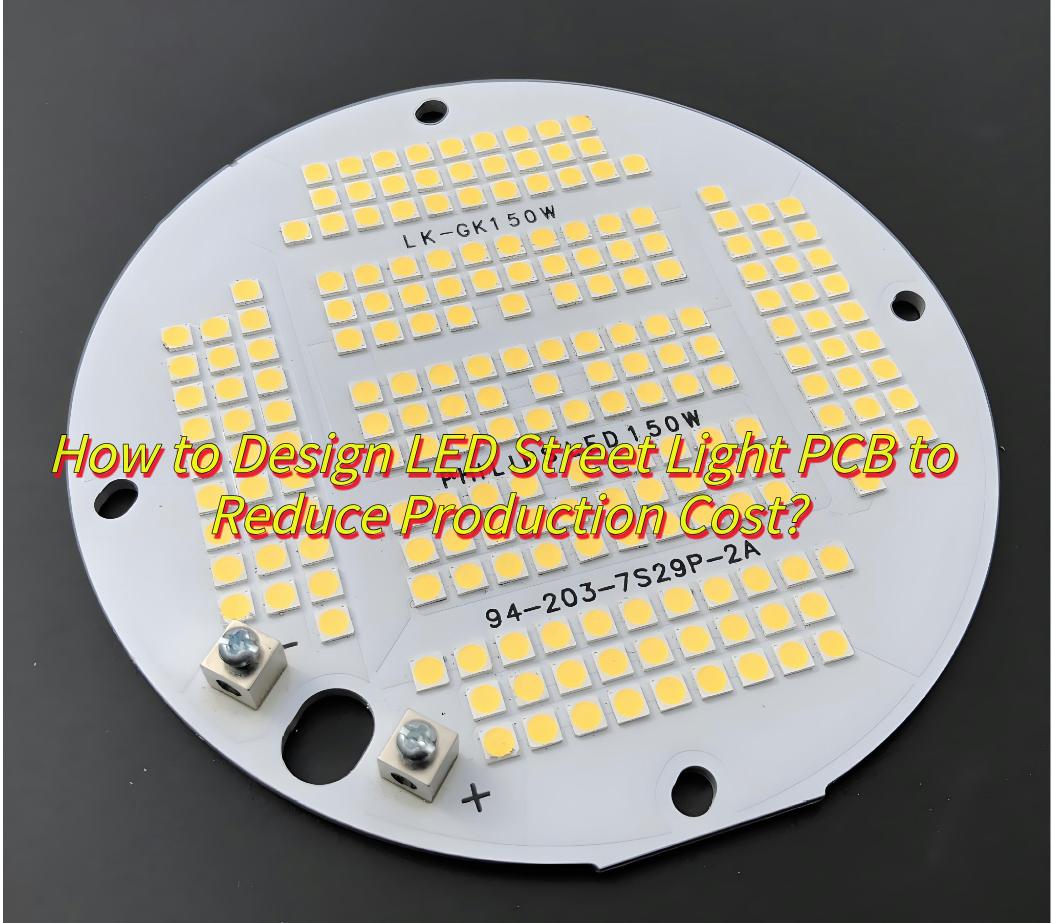
How to Design LED Street Light PCB to Reduce Production Cost?
Confirm that the manufacturer has ISO 9001 quality management certification and IP65/67 waterproof and dustproof certification to ensure production specifications and product reliability;
Give priority to manufacturers that have passed UL international safety certification to meet export market needs.
Technology and production capacity
Investigate the automation level of the production line (such as SMT placement machines, AOI inspection equipment) to improve efficiency;
Verify customized R&D capabilities (such as the design of heat dissipation solutions for 30W+ high-power street lights).
Quality and cost control
Require manufacturers to provide RoHS material certification and batch-level high and low temperature cycle test (-40°C~85°C) reports;
Obtain itemized quotations (PCB unit price, patch processing fee), and negotiate a tiered price of 500 pieces to reduce costs.
Delivery and supply chain management
Confirm the standard delivery time ≤ 20 days, monthly production capacity ≥ 10,000 pieces, and ensure the stability of batch orders;
Factory inspection and sample verification
Inspect the details of the workshop ESD protection, temperature and humidity control, etc.;
Measure the full-load temperature rise (ΔT ≤ 15°C) and the light decay rate (≤ 3%) of the sample.
What Factors Affect LED Street Light PCB Pricing?
1. Material and process
Substrate material: High thermal conductivity materials (such as 2oz copper substrate) or honeycomb thermal conductive structure can improve heat dissipation efficiency, but the material cost increases by 20-30%;
Environmental compliance: Lead-free solder and flame-retardant copper clad laminate (FR-4) that meet RoHS standards are 15-20% more expensive than ordinary materials.
2. Production complexity
Number of layers and wiring density: The processing fee of PCBs with more than 4 layers increases by 30-50% due to impedance control and heat dissipation requirements;
Testing requirements: AOI/X-ray full inspection and batch-level high and low temperature cycle testing (-40°C~85°C) improve reliability, but the testing cost accounts for 8-12%.
3. Heat dissipation and circuit design
Driver solution: Constant current driver chip (such as TI/Infineon solution) is 25% more expensive than the basic solution, but can reduce the risk of light decay;
Thermal management design: Copper substrate + ceramic filling hole structure can control the full load temperature rise within 15°C, and the design fee increases by 10-15%.
4. Certification
International certification: PCB manufacturers that have passed UL/CB certification generally quote 5-8% higher due to process audit costs.
5. Order size and delivery
Bulk discount: Orders of more than 1,000 pieces can enjoy a 5-10% step-by-step price reduction, while small batch custom orders have a 30% higher unit price;
Delivery time compression: The price difference between 15-day standard delivery and 7-day expedited delivery can reach 12-15%.
FAQs of LED Street Light PCB Manufacturing
Q1: How do you ensure consistent quality in bulk orders?
A1: EBest Circuit (Best Technology) employs statistical process control (SPC) and 100% AOI (Automated Optical Inspection) to maintain low defect rates.
Q2: Can you handle custom designs with unique shapes or cutouts?
A2: Yes. Our CNC routing and laser cutting systems support complex geometries with ±0.2mm precision.
Q3: What certifications do your materials hold?
A3: We use UL-certified aluminum substrates and IEC-grade dielectric layers, ensuring compliance with EU and North American safety standards.
Q4: Do you offer waterproof conformal coatings?
A4: Yes, We apply acrylic or silicone coatings (IP67/IP68) to protect PCBs from moisture and chemical exposure.
Q5: What’s your typical lead time for 1,000-unit orders?
A5: Standard production takes 7–10 days, with expedited options available for urgent projects.
In conclusion, that’s all about LED street light PCB how to select a reliable LED street light PCB manufacturer with design service, if you have anything else needs to help, welcome to leave a message below this blog.
Just as its name implies, LED PCBs are specialized circuit boards designed to power and support LED (Light Emitting Diode) lights. These PCBs must manage heat efficiently and distribute power effectively to handle the electrical load and heat generated by LEDs. They provide the essential platform for mounting LEDs and connecting them to other electronic components. LED PCBs are used in a wide variety of applications, ranging from basic light fixtures to sophisticated lighting systems in automotive, signage, and consumer electronics.
Typically, LED PCBs are made from materials with high thermal conductivity, such as aluminum or copper, to effectively manage heat. The design of these boards varies depending on the type of LED chips, such as surface-mount (SMD) LED or through-hole. LED PCBs also come in various forms, including flexible, rigid, and semi-flexible options, each tailored to specific lighting applications. Regardless of the type, careful attention to the LED PCB design is essential to achieve optimal performance and efficiency.
LED PCB Design Basics
Actually, the basics of a LED PCB design is a deep understanding and practice of both electrical and thermal engineering principles. LED circuit boards differ from standard PCBs because they must support higher currents and dissipate more heat. Therefore, careful planning is required in selecting materials, components, and layout strategies to ensure long-term reliability and efficiency.
At its core, LED PCB design focuses on three main factors:
Thermal Management: LED devices generate heat, which can damage the components if not managed correctly.
Current Distribution: The PCB must handle the specific current requirements of each LED.
Power Design: Since LEDs operate at specific voltages and currents, the power supply must be designed to match these needs.
5 Commonly Used LED PCB Design Software
Before starting a LED PCB design, let’s know the commonly used software during the design process. These tools can help to handle complex circuits, including component placement, routing, and thermal management. It can save much time and money for us.
1. Altium Designer
Altium is a powerful tool known for its user-friendly interface and extensive design features. It offers comprehensive options for both schematic capture and PCB layout, it is a popular choice for professional LED PCB design.
2. Eagle
For smaller business and hobbyists, Eagle is a good choice because it offers an easy-to-use interface and a solid set of features to creating LED circuit boards without steep learning curves.
3. KiCad
KiCad is an open-source and free PCB design tool that is well-regarded for its flexibility and cost-effectiveness. It’s suitable for users who need a more customizable design solution.
4. Mentor Graphics PADS
PADS is well-suited for complex and high-performance PCB designs, particularly for high-frequency LED applications that demand precision and accuracy.
5. DipTrace
DipTrace offers a combination of schematic capture and PCB layout in a user-friendly environment. Its drag-and-drop interface helps reduce design time.
How to Design a LED Circuit Board? – Step by Step
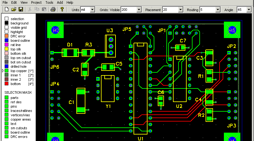
A good LED circuit board is based on a good LED PCB design. When you have a clear ideal and thought about your LED PCB, then you can start designing your PCB. Same as normal FR4 PCB, the LED PCB design starts from schematic drawing – layout – trace wiring – power integrity checking.
1. LED PCB Schematic Diagram Design
This diagram serves as the foundation for the PCB design, so any errors at this stage can lead to problems in the final board. Using a reliable schematic diagram tool to draw your circuit accurately and efficiently. Additionally, avoid overly complex circuits with multiple connections in a single diagram. Keeping the schematic clear and simple will make troubleshooting easier and ensure the design process progresses without issues.
2. LED PCB Layout
Once the schematic is finalized, the next step is the PCB layout. This involves placing the components and routing the traces that will carry the electrical signals to power the LEDs. This stage directly impacts the PCB’s performance, so precise planning and routing are essential. During the pcb layout, remember these tips:
High-power LEDs should be placed in areas with good airflow or close to heat sinks. It’s also important to keep resistors and power supply components away from heat-sensitive parts.
To ensure that the traces can handle the required current without overheating, you need to calculate the trace width. Tools like IPC-2221 or use our Online PCB Trace Width Calculators can help determine the appropriate width based on the current and copper thickness used in the PCB. For example, a 1oz copper PCB might need a trace width of 2mm to carry a 2A current safely.
Using separate power and ground planes to avoid voltage drops and noise. Power planes provide a low-resistance path for high-current traces, while ground planes help with signal integrity and reduce noise.
Thermal vias are often used to transfer heat from the LED to the PCB’s back layers or heat sinks. For high-power LEDs, these vias must be carefully placed to ensure that heat is efficiently dissipated.
3. LED PCB Wiring
Wiring refers to the creation of the electrical traces that connect the components on the PCB. Compared with FR4 PCB, wiring an LED circuit board is generally straightforward, but attention to detail is essential, particularly when it comes to the lead lengths of each component in the LED PCB design. Typically, the cathode lead is the shortest and connects to the same socket as the anode. Similarly, the resistor should be connected to the anode’s socket, and the other wire, often red or black, should follow the same principle.
Here are some important LED PCB design guidelines for wiring the LED circuit board:
Component Selection: Before starting the design, choose the LED components based on the specific requirements of your LED circuit board.
Plan the Wiring Layout: Carefully plan your LED PCB wiring layout and double-check its accuracy before proceeding with the wiring process.
Via and Trace Optimization: Minimize the use of vias, as they can introduce resistance and inductance. If vias are necessary, ensure they are appropriately sized and placed to handle the current.
Proper Grounding: Ensure that all LED components in the PCB design are correctly grounded to the circuit board.
Wire Gauge Selection: Use the appropriate wire gauge for each section of the LED PCB, depending on the current load in each path.
Prevent Interference: If any wire leads cross over other conductive paths, clamp them securely to prevent interference or accidental contact with other components.
Heat Shrinking: Apply heat shrink tubing to exposed wire junctions to protect against interference and reduce the risk of short circuits.
Signal Routing: Ensure that signal traces (such as PWM signals in RGB LED designs) are routed separately from power traces to prevent interference and maintain signal integrity.
Continuity Check: Before powering up your LED PCB, check for continuity throughout the circuit to ensure everything is connected properly.
Power Source: Always use an approved power supply when connecting external voltage to the LED PCB.
Final Check: Before applying power, make sure there are no short circuits, open circuits, reverse polarity issues, or incorrect component placements.
Test the LEDs: Regularly test the LEDs to ensure optimal performance under various operating conditions.
4. LED PCB Power Design and Analyzing
LED PCBs often require specific power designs to prevent overloading and ensure efficient energy consumption. You must consider the input voltage and how power will be distributed across the board. Proper power analysis ensures that the PCB operates within its designed power specifications.
5. LED PCB Signal Integrity Analysis
Signal integrity is an essential aspect of LED PCB design, particularly for high-speed or high-frequency LED applications. Ensuring that signals are not distorted during transmission will improve the overall performance and efficiency of the LED circuit. This phase involves simulating the behavior of the circuit to ensure it performs optimally under various conditions.
Simulate circuit behavior: Use specialized tools to simulate how the circuit will behave under different loads and environmental conditions.
Ensure minimal noise: Check for potential interference or noise in the circuit that could affect LED performance.
LED PCBs come in various shapes, such as round, rectangular, or custom forms, depending on the final application. For example, LED strip PCBs are often flexible and come in long, narrow shapes, while LED array PCBs may need to accommodate multiple LEDs in a compact rectangular form.
2. Thermal Management
Effective thermal management is one of the most critical considerations when designing an LED PCB. LEDs generate heat during operation, and without proper heat dissipation, performance can degrade quickly, leading to shorter lifespan and possible failure. Aluminum PCBs are often used in LED designs due to their excellent thermal conductivity. Alternatively, copper-clad PCBs may be chosen for high-power applications to ensure that heat is efficiently transferred away from the LEDs.
3. Current Control
Each LED needs a current-limiting resistor to avoid excessive current that could damage the LED. In high-power LED applications, constant current drivers are often used to regulate the current supply.
4. Component Placement
Components should be arranged to minimize heat buildup, reduce interference, and maintain a clean signal path.
LED Positioning: Place high-power LEDs in areas with better airflow or near heat sinks. Ensuring adequate space around each LED can help manage heat more effectively.
Resistor and Capacitor Placement: Resistors and capacitors should be placed near the LEDs to minimize the impact of parasitic inductance or resistance. Proper placement also improves the overall efficiency of the circuit and minimizes signal loss.
5. Layout Optimization
The layout takes into account signal integrity and power integrity. In the layout, you need to follow the following principles:
Power and signal lines should be as wide as possible to reduce resistance and inductance.
The length of the power and signal lines should be as short as possible to reduce signal delay and noise.
Sensitive signal lines should be kept away from noise sources, such as motors, switches, etc.
The arrangement of power and signal lines should take into account the issue of electromagnetic interference (EMI).
LED PCB Design Success Cases at EBest Circuit (Best Technology)
EBest Circuit (Best Technology) is a leading LED PCB manufacturer in Shenzhen China, a city famous of its well-developed electronics industry. Since established in 2006, we have rich experiences in metal core PCB manufacturing, including every aluminum LED PCB and copper core LED PCBs. Different with FR4 PCB, the key manufacturing difficulty of LED PCB is its lamination between dielectric and base, we deeply know its importance, so we set a separate lamination department with experience operators to solve this problem. Additionally, our factory equipped with advanced manufacturing machines to improve our capacity and efficiency. With strong R&D team, we are able to offer better LED PCB design solution to our customers, ensure one-time prototype success. Below, we highlight several success cases that demonstrate how we served our customers.
1. High-Power LED PCB Design for Street Lighting
Customer Challenge:
One of our clients, a leading provider of outdoor lighting solutions, approached us with a high-power LED streetlight project. The primary difficulty they faced was heat dissipation. LED streetlights generate a significant amount of heat, and without effective thermal management, the lifespan of the LEDs would dramatically decrease, leading to frequent failures and increased maintenance costs. The client needed a robust and reliable LED PCB design that could handle the heat produced by high-power LEDs while ensuring energy efficiency and long operational life.
Our Solution:
We suggested aluminum-based PCBs since it has better thermal conductivity than FR4 PCB. To improve heat dissipation further, we added thermal vias and designed the layout to maximize the heat transfer from the LEDs to the surface. In this way, heat sinks can be removed to save some spaces and costs. Additionally, we incorporated constant-current drivers to maintain a stable power supply and prevent current surges that could further exacerbate the heating issue.
Outcome:
Our high-power LED PCB design successfully met the client’s stringent requirements. The energy-efficient design led to reduced operational costs, and the improved thermal management extended the lifespan of the streetlights.
2. RGB LED PCB Design for Swimming Pool
Customer Challenge:
A client in the entertainment industry required a RGB LED PCB for dynamic visual displays in a large-scale concert venue. The biggest challenge was ensuring color accuracy, brightness consistency, and signal integrity across a large array of LEDs. Given the complexity of RGB mixing, the client needed a design that would maintain color uniformity and prevent color distortion or flickering, especially during high-speed color transitions.
Our Solution:
We tackled the signal integrity problem by carefully routing the RGB signal traces to minimize interference and crosstalk. We also integrated pulse-width modulation (PWM) to control brightness, allowing for smooth color transitions and fine-tuned brightness control. The PCB layout included dedicated ground planes to prevent noise from power traces and ensured that the voltage regulators could handle the high current demands without introducing voltage fluctuations that could impact color performance.
Outcome:
The final design ensured vibrant, accurate colors and consistent brightness, even across large areas of the display. The client was able to achieve visually stunning, seamless light transitions for dynamic effects, greatly enhancing the overall viewing experience.
3. SMD LED PCB Design for Compact Devices
Customer Challenge:
A customer in the consumer electronics industry needed an SMD LED PCB for a handheld device. The main challenge here was to design a compact PCB that could handle the power requirements of high-brightness LEDs without compromising the device’s sleek profile. Additionally, the customer faced the issue of heat buildup in such a confined space, which could negatively affect both performance and lifespan.
Our Solution:
To accommodate the client’s space constraints, we employed fine-pitch SMD LEDs and used multi-layer PCB technology to stack components vertically. This allowed us to maximize the use of the available space while maintaining efficient current flow and power distribution. For heat dissipation, we incorporated thermal vias and copper planes to spread heat away from the LEDs. Our design also included current-limiting resistors and voltage regulators to stabilize the power supply to each LED, ensuring consistent performance despite the small size of the PCB.
Outcome:
The customer was extremely satisfied with the reliable, long-lasting solution, which became a cornerstone feature of their product line.
4. Simple LED PCB Design for Residential Lighting
Customer Challenge:
A client in the home lighting industry required a simple LED PCB for mass production of affordable, energy-efficient residential lighting solutions. The challenge was to design a PCB that was both cost-effective and reliable, while ensuring that the LEDs would not overheat or burn out prematurely, especially in long-duration use cases.
Our Solution:
For this project, we designed a single-layer PCB to minimize costs while maintaining functionality. We incorporated current-limiting resistors to protect the LEDs and used low-cost components that could be easily sourced for mass production. Thermal considerations were addressed by optimizing the component placement and providing ample space around the LEDs for heat dissipation. We also ensured the design could handle voltage fluctuations by incorporating a voltage regulator.
Outcome:
The design resulted in a highly affordable, yet durable LED PCB that was well-suited for high-volume production.
5. Flexible LED Strip PCB Design for Custom Installations
Customer Challenge:
A client involved in decorative lighting for both residential and commercial spaces required a flexible LED strip PCB that could be easily bent and shaped around various installations. The major hurdle was ensuring consistent power distribution along the strip while maintaining a compact and flexible design. The client also needed the strips to withstand outdoor conditions without compromising on performance.
Our Solution:
We designed the flexible LED PCB using polyimide film for its excellent flexibility and durability. To ensure uniform brightness across the entire length of the strip, we used constant voltage circuits and low-resistance traces to minimize power loss. We also applied encapsulation to protect the PCB from environmental factors such as moisture, UV rays, and physical wear and tear.
Outcome:
The resulting LED strip was not only flexible but also highly durable and weather-resistant, making it suitable for both indoor and outdoor use. The customer was able to offer a customizable, high-quality lighting solution that could be used in a wide range of applications, from commercial signage to home decor.
FAQs
Q1: Are the via’s important for the thermal conduction?
From the via’s perspective, the via can be helpful in thermal conduction. At the same time, it is not that more heat dissipation through holes is better. The design of Via needs to be followed the minimax distance between holes. From the metal core material, the copper material is better than aluminum core in same situation. And sinkpad copper core PCB is better than copper core PCB. Because the convexity pad will be helpful in thermal conductivity. From the dielectric film, the 3W material is best. 2W material is better than 1W material. From the design of metal core PCB, the larger the area of solder mask opening means the larger the exposed copper surface outside, and the better the heat dissipation effect.
Q2: Does the dielectric in MCPCB cause problems at high temperatures?
The dielectric in MCPCB will cause problems at high temperatures, and the dielectric layer of MCPCB is the bottleneck of high temperature, because the Tg value of the layer is only 130℃.
Q3: What is the thickness of the thermal conductivity?
0.8W/m.k,Thickness=50-75um
1.0W/m.k,Thickness=75-100um;
1.5W/m.k,Thickness=100um
2.0W/m.k,Thickness=100-125um;
3.0W/m.k,Thickness=125-200um
For the breakdown, it is bigger when the line space is wider and the dielectric layer is thicker. Normally, the copper thickness is 10Z and 2OZ and surface finishing is HASL(LF), ENIG and OSP.
Q4: Can the aluminum be made as the base of sinkpad MCPCB?
Actually, the sinkpad can only use copper as the base. Because the SinkPad will etch the copper base into convex platform with Copper Etching Solution, then hollow out the Double Layer FR4 PCB, and do lamination with the convex platform. However, regarding of current technical conditions, since aluminum or aluminum alloy cannot directly react with acid, the reaction process is too complex and difficult to control, which will increase the difficulty of etching the LED pad platform. Considering the scrap rate, the process of etching LED pad platform with aluminum is more complex and the overall cost is higher.
Q5: It is possible dielectric + top metal layer to be >500um for wire bonding?
The dielectric layer and metal layer don’t affect the wire bonding, it depend on ENEPIG thickness, we do a lot of this kind of boards for our customers, as long as the do it with 3u”, then it is very good for wire bonding. If you insist on needing dielectric + top metal layer to be >500um, then the copper thickness need to be 10 OZ(350um), the price will be very high.
Are you looking for a reliable LED round PCB manufacturer? Let’s learn about structure and application of LED round PCBs as well as how to select a good LED round PCBs supplier.
EBest Circuit (Best Technology) focuses onLED round PCBmanufacturing, with high-density layout and aluminum/copper substrate heat dissipation technology, and has passed ISO/UL/IPC certification to ensure that the process can meet international standards. In addition, we provide one-stop service (from design to mass production), with the fastest 24-48 hours prototyping, combined with mixed substrate solutions and batch tiered quotations, reducing costs by 20%. Thermal cycle testing and fully automatic testing equipment are used to ensure the reliability of products in extreme environments. Choose us, and you will be ahead in technology, efficiency, and quality. Feel free to contact us sales@bestpcbs.com
What Is an LED Round PCB?
AnLED Round PCBis a circular printed circuit board designed to mount LEDs in a compact, space-efficient layout. Unlike traditional rectangular boards, its shape allows for innovative lighting designs in products requiring curvature or minimal footprint. Common variants include the 1.5-inch LED Round PCB Board (ideal for wearables) and Addressable Micro LED Round PCB (enabling pixel-level control for dynamic displays).
What Are Structure of LED Round PCB?
A typical Round LED PCB consists of:
Base Material: FR-4 (standard) or aluminum (for heat dissipation).
Copper Layer: Etched conductive pathways for electrical connectivity.
Solder Mask: Insulating layer to prevent short circuits.
Silkscreen: Component labels for assembly accuracy.
LED Mounting Pads: Precision-placed to ensure uniform light distribution.
Confirm that the manufacturer has round LED PCB special technology, including thermal management system design, multilayer board (4-16 layers) production capacity and precision drilling process, and requires the use of advanced equipment such as automated assembly lines and LDI exposure machines.
Require ISO 9001 certification, provide AOI/X-ray inspection reports, and verify the quality of sample solder joints, component alignment accuracy and heat dissipation performance.
Ensure the use of LED-specific substrates (such as aluminum substrates, CEM-3), prohibit non-certified components, and the thickness of copper foil must meet the high current carrying requirements.
Support 24-hour rapid prototyping, seamless switching from small batches to large batches, and provide design for manufacturability (DFM) optimization services.
Compare the price-marking scheme (including surface treatment costs such as HASL/ENIG), and negotiate long-term cooperation ladder prices and free first sample policies.
Confirm to provide 24-hour technical support and 48-hour response to after-sales issues, and give priority to integrating the whole process of design-procurement-assembly service providers.
How to Reduce the Production Cost of LED Round PCB board?
Design Optimization: Minimize board size and layers; reuse standardized layouts to cut material and design costs.
Material Selection: Use cost-effective substrates (e.g., CEM-3), optimize copper thickness, and prioritize generic LEDs.
Testing & QC: Validate with prototypes early and implement SPC to reduce defects.
Supply Chain: Bulk purchase materials and source locally to lower logistics costs.
LED-Specific: Adopt COB integration to eliminate packaging and optimize thermal design with aluminum-core substrates.
How Does Addressable Micro LED Round PCB Achieve Pixel-Level Control?
This is how addressable micro LED round PCB achieve pixel-level control:
Integrated CMOS Control-Each Micro LED connects to a dedicated CMOS driver for individual control, enabling ultra-fast response (25 ns) and low power use (5 mW/pixel). Shared P-electrode and isolated N-electrode structures ensure precise pixel activation.
High-Density Circuit Design-Precision drilling (≤50 μm holes) and multi-layer stacking (4-16 layers) achieve 4 μm pixel spacing (5100 PPI). Flip-chip bonding integrates LEDs and drivers, reducing signal delays.
Digital Signal Systems-Single-wire protocols (e.g., WS2811/WS2812) cascade RGB data to driver ICs for dynamic color control. Active drivers (TFT/NMOS) offer 450 MHz bandwidth for smooth brightness/grayscale adjustments.
Precision Manufacturing-Laser/elastic transfer methods place LEDs on PCB pads with >99% accuracy. Transparent epoxy encapsulation minimizes light interference and improves heat management.
Signal Stability-LVDS reduces noise; flexible polyimide substrates prevent circuit damage in curved layouts. Isolated power zones protect signal integrity between digital/analog components.
Smart Software Integration-Custom algorithms (PWM, gamma correction) sync with hardware via SPI/I2C for 240 Hz refresh rates. Backup circuits replace failed pixels automatically to maintain display quality.
Can 1.5 inch LED Round PCB Board Be Customized?
Yes, 1.5-inch LED round PCB boards can be customized and other sizes can be customized. Suppliers like EBest Circuit (Best Technology) offer tailored designs for circular layouts, including aluminum or copper-core materials for heat dissipation and signal integrity optimization. Customization options cover touchscreen integration, high-density LED arrangements, and compatibility with standard mounting structures.
To sum up, that’s all about definition, structure, application of round LED PCB, as well as how to select a trusted LED PCB round board manufacturers, how addressable micro LED round PCB works and if 1.5 inch LED round PCB board be customized. If you have any other issue for round LED PCBs, please leave a message below this blog.