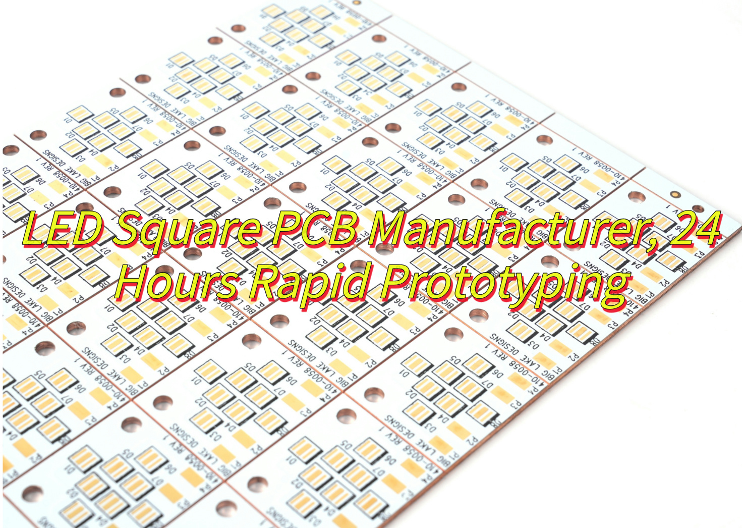
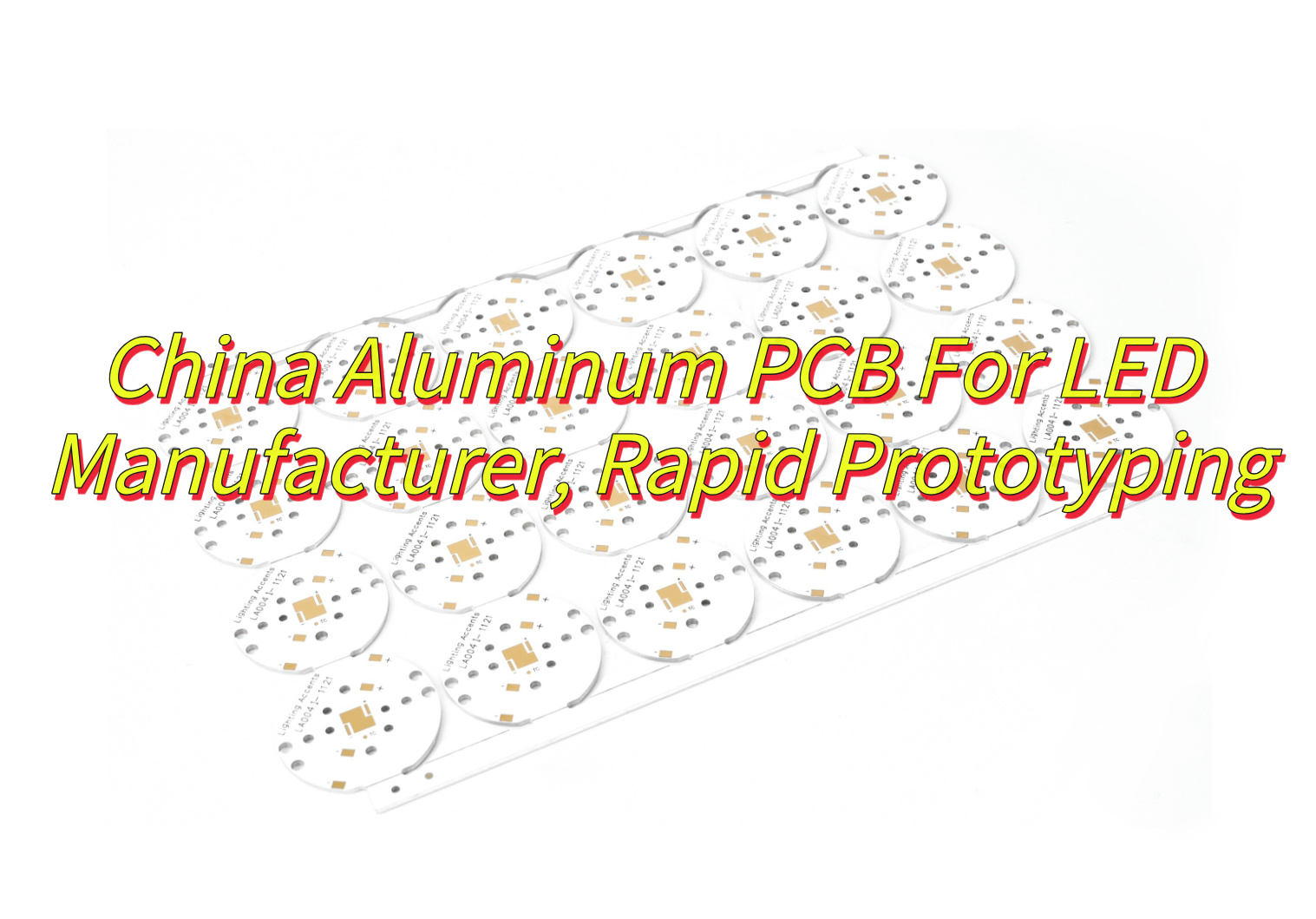
When you’re in the market for a metal core PCB manufacturer, finding the right one can make a big difference. From ensuring the efficiency of heat dissipation to maximizing performance, metal core PCBs (MCPCBs) offer unique benefits in the world of electronics. As more companies look to enhance their products with these specialized PCBs, the need for a reliable and skilled manufacturer grows.
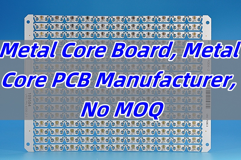
EBest Circuit (Best Technology) is a metal core PCB manufacturer compliance with ISO9001, ISO13485, IATF16949, AS9100D, UL, REACH, RoHS. With MOQ-free, EBest Circuit (Best Technology) is an original factory for SinkPad PCB, Aluminum PCB Manufacturing. Our competitive edges lie in zero MOQ, 2-3 weeks lead time policy, and 24/7 engineering support. We operate strategically located SMT factories in China and Vietnam, offering full SMT assembly capabilities and mixed assembly advantages. If you need metal core PCB instant quote, welcome to contact us at sales@bestpcbs.com.
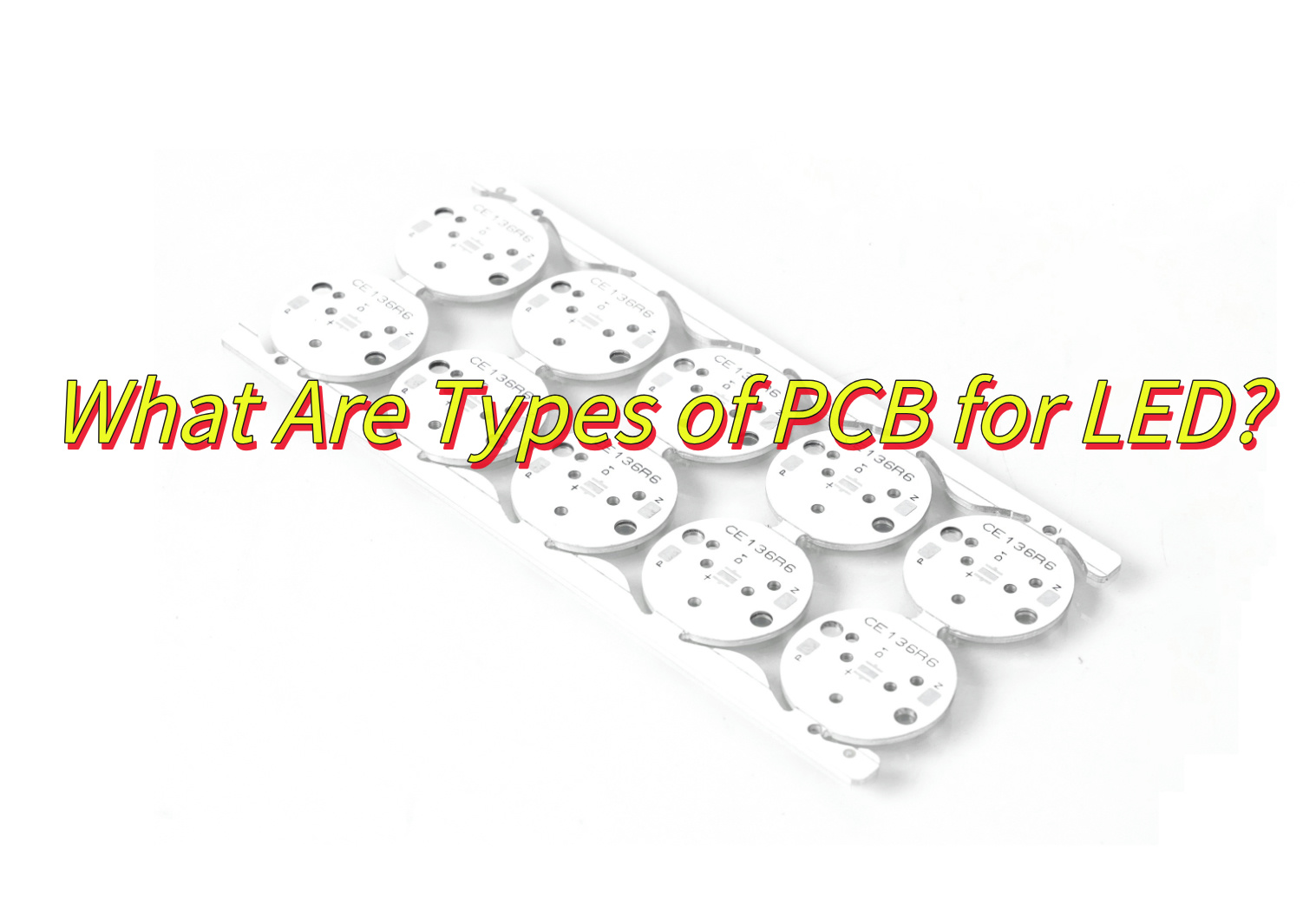
What Metals Are in Circuit Boards?
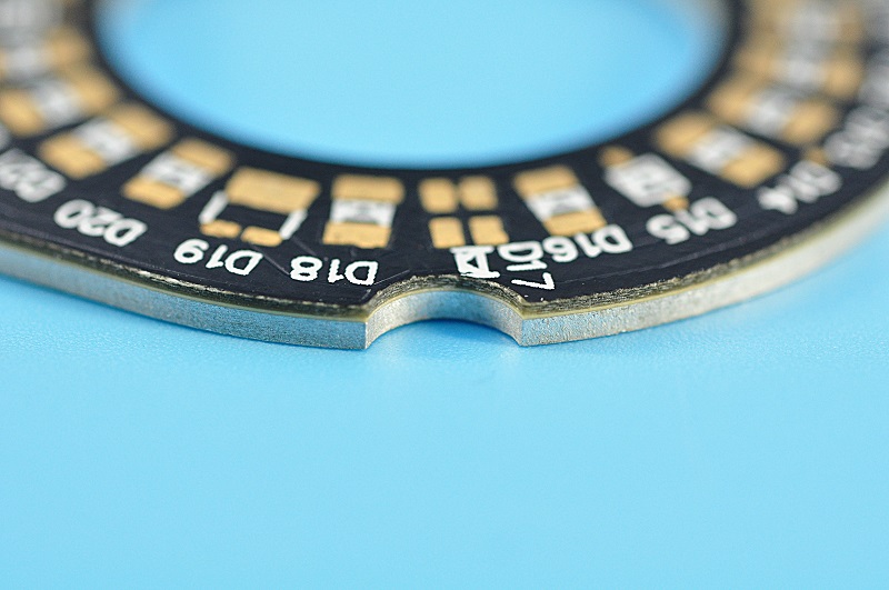
When discussing metal core PCBs, it’s essential to understand the types of metals commonly used in their construction. While standard PCBs use materials like fiberglass and copper, metal core PCBs take it a step further by incorporating metals such as aluminum, copper, and steel.
- Aluminum is the most widely used metal in MCPCBs due to its excellent thermal conductivity, lightweight nature, and cost-effectiveness.
- Copper is also used for its superior thermal performance, making it ideal for high-performance applications like power electronics and LED lighting.
- Steel might be used in certain designs for added strength, especially in cases where durability is a top priority.
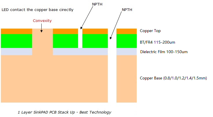
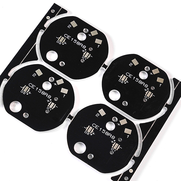
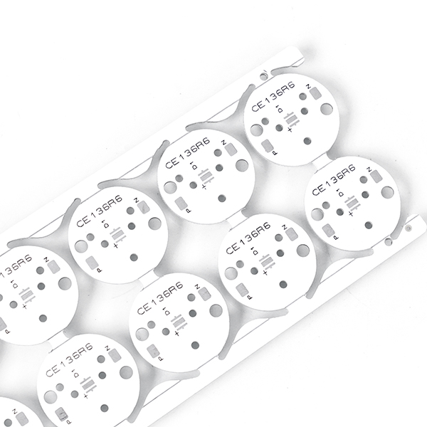
These materials help in efficiently managing heat, which is critical for ensuring the longevity and reliability of electronic devices. EBest Circuit (Best Technology) offers rigorous quality inspection to metal core board. We assure you that there is no MOQ requirement, and all metal core PCB production is IPC standards compliance.
How Are Metal Core Circuit Boards Manufactured?
The metal core PCB manufacturing process is a specialized procedure designed to optimize the thermal conductivity of the board. The general steps involved are:
- Material Selection: Depending on the application, materials like aluminum or copper are chosen for the core layer. These materials are selected based on the need for heat dissipation and cost considerations.
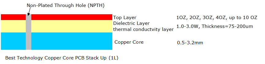
- Layering: The core metal (e.g., aluminum) is coated with a dielectric insulation layer, followed by a copper circuit layer. This structure ensures efficient heat transfer from components to the metal core.
- Drilling and Plating: Holes are drilled through the layers, followed by insulation treatment (e.g., resin filling) to isolate the metal core. Copper plating is then applied to form conductive vias and pathways.
- Etching: The copper layer is etched to create precise circuit traces and pads.
- Final Testing: Rigorous thermal cycling, electrical, and reliability tests are conducted to validate performance under demanding conditions.
The precision and quality of these steps are vital to producing an effective metal core PCB that will perform under challenging conditions.
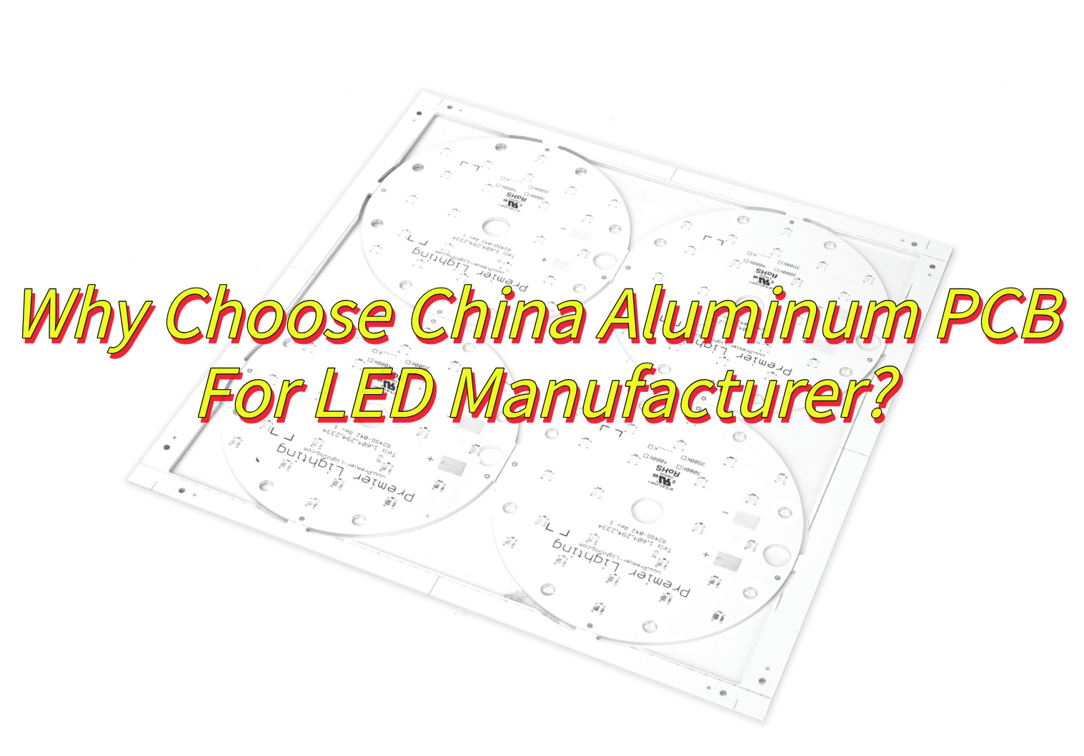
Metal Core PCB Manufacturer China
China has long been a global leader in PCB manufacturing, and the demand for metal core PCBs has grown alongside the expansion of industries such as automotive, consumer electronics, and LED lighting. The country’s extensive manufacturing capabilities, combined with competitive pricing, make it an attractive destination for companies seeking reliable metal core PCB manufacturers. In this section, we will explore the top metal core PCB manufacturers in China who specialize in delivering high-quality products that meet global standards.
EBest Circuit (Best Technology)
- EBest Circuit (Best Technology) is one of China’s top PCB manufacturers, with a strong reputation for delivering high-quality metal core PCBs at high quality. Our comprehensive services range from design assistance to full-scale production, catering to industries such as LED lighting, power electronics, and medical devices.
Shenzhen Sesa Tech Co., Ltd.
- Sesa Tech is a well-established manufacturer of various PCBs, including metal core PCBs. They focus on providing custom solutions for industries like automotive, telecommunications, and consumer electronics. Their production facility is equipped with cutting-edge technology, and they are known for offering efficient turnarounds on high-volume orders.
When looking for a metal core PCB manufacturer in China, these companies provide a combination of cost-effective solutions, advanced technology, and reliable production. Whether you’re aiming for high-volume production or quick prototyping, China remains a key player in the global PCB manufacturing landscape.
Metal Core PCB Manufacturer Bangalore
Bangalore, known as India’s tech hub, is home to a growing number of PCB manufacturers who specialize in metal core PCBs. The city’s robust engineering expertise, coupled with affordable labor costs, makes it an ideal location for sourcing high-quality PCBs. In this section, we’ll highlight some of the leading metal core PCB manufacturers in Bangalore that can meet the needs of various industries such as automotive, aerospace, and LED lighting.
V-Tech PCB
- V-Tech PCB is a well-established manufacturer in Bangalore, specializing in a wide range of PCB products, including metal core PCBs. With an emphasis on quality control and precision, V-Tech serves industries like automotive, telecommunications, and industrial electronics. Their state-of-the-art manufacturing facility ensures that every PCB meets global standards.
Eagle Circuits
- Eagle Circuits has been a trusted PCB manufacturer in Bangalore for over a decade. Their metal core PCB offerings are highly regarded for their superior heat dissipation properties, making them ideal for applications such as power electronics and high-power LEDs. Eagle Circuits is known for their flexible manufacturing processes and quick delivery times.
Flextronics
- Flextronics, a global player in the electronics manufacturing industry, has a significant presence in Bangalore. They offer metal core PCBs for a variety of applications, with a strong focus on innovation and quality. Their experience in producing high-performance PCBs for the automotive and industrial sectors ensures that their products meet stringent specifications.
Bangalore offers a growing number of metal core PCB manufacturers that provide a blend of technical expertise, cost-effective solutions, and quick delivery. Companies looking for reliable and high-quality manufacturers can rely on Bangalore’s rich pool of experienced manufacturers.
Metal Core PCB Manufacturer in Delhi
Delhi, as the capital of India, has emerged as an important hub for PCB manufacturing, including metal core PCBs. The city’s strategic location, coupled with access to a skilled workforce and advanced manufacturing technology, makes it a key destination for companies seeking high-quality PCBs. In this section, we’ll explore some of the top metal core PCB manufacturers in Delhi who offer a wide range of products tailored to industries like automotive, medical devices, and electronics.
PCB Power Market
- PCB Power Market is a leading PCB manufacturer in Delhi, specializing in both standard and metal core PCBs. They provide high-quality PCBs for a variety of industries, including automotive, lighting, and industrial electronics. Their advanced manufacturing process ensures precision and durability, especially in heat-sensitive applications.
Atotech India Pvt. Ltd.
- Atotech is a global leader in PCB manufacturing with a significant presence in Delhi. They provide metal core PCBs designed for high-heat applications. Known for their cutting-edge technology and adherence to international quality standards, Atotech serves industries such as medical devices, automotive, and telecommunications.
Deltronics
- Deltronics is a reputable manufacturer in Delhi known for their metal core PCBs that offer excellent thermal management. They specialize in custom PCBs designed to meet the unique needs of clients, particularly in power electronics and LED applications. Deltronics is committed to delivering high-quality products with fast turnaround times.
Delhi is home to a variety of metal core PCB manufacturers offering high-quality, reliable, and cost-effective solutions for various industries. Whether you are in need of high-performance metal core PCBs for LED applications or power electronics, Delhi manufacturers provide competitive options that meet international standards.
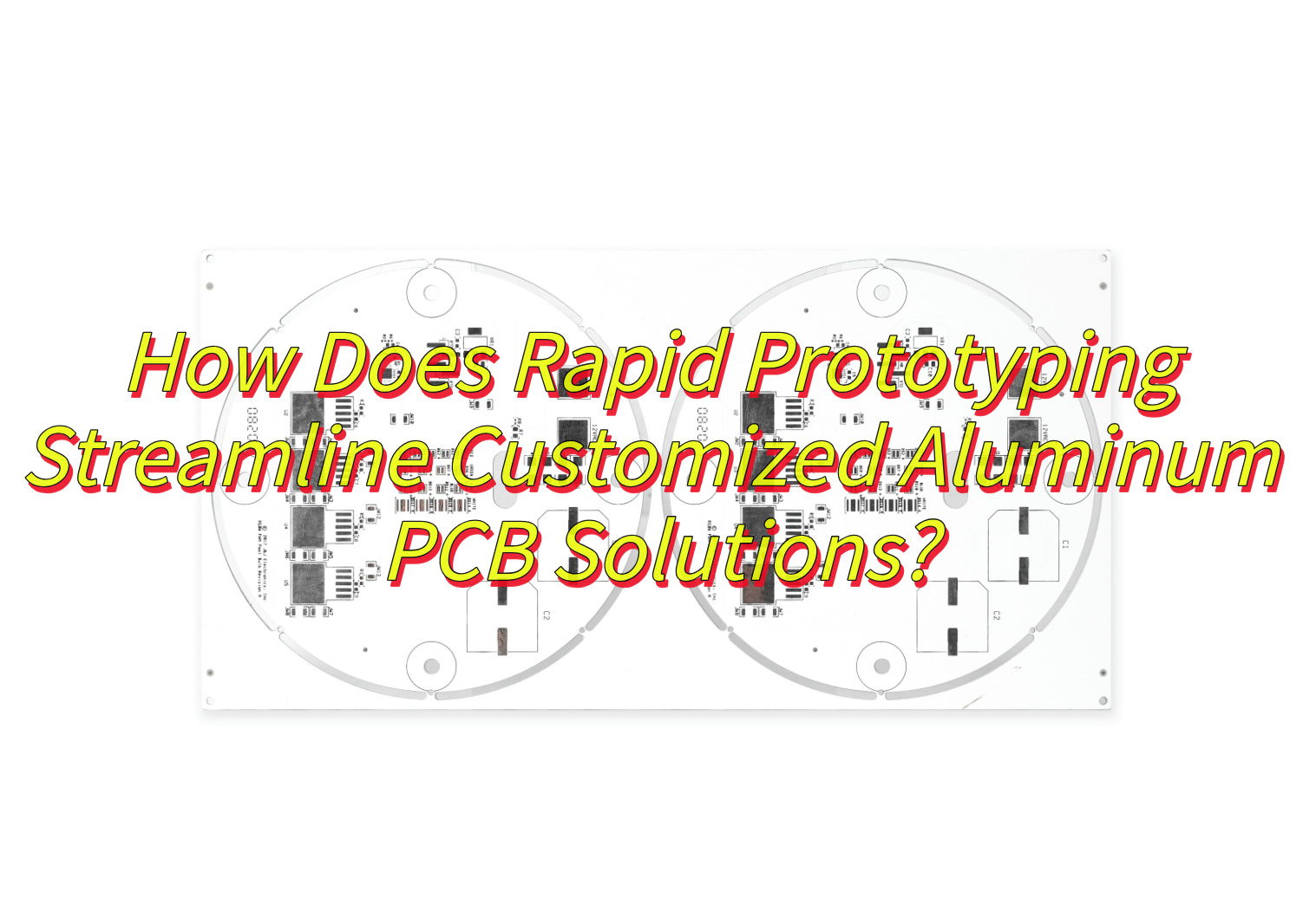
How to Evaluate and Select the Best Metal Core PCB Manufacturer?
Choosing the right metal core PCB manufacturer involves evaluating several key factors:
- Experience and Expertise: Ensure that the manufacturer has a proven track record in producing MCPCBs for the specific applications you need.
- Certifications: Look for manufacturers with relevant certifications, such as ISO9001 and IATF16949, which demonstrate a commitment to quality control.
- Customization: The ability to design and manufacture custom MCPCBs tailored to your specific needs is crucial, especially for complex projects.
- Cost and Lead Time: Compare prices and lead times between manufacturers to ensure you’re getting the best value without compromising on quality.
- Customer Service and Support: A reliable manufacturer should offer excellent customer service, including post-production support and assistance with troubleshooting.
Taking the time to consider these factors will ensure that you select the best partner for your metal core PCB needs.
Why Should You Choose EBest Circuit (Best Technology) as Your Metal Core PCB Manufacturer?
When it comes to metal core PCB manufacture, EBest Circuit (Best Technology) stands out as a trusted partner. Here are a few reasons why we are your best choice:
- Quality: We are committed to the highest standards of quality control. Our metal core PCBs are rigorously tested to ensure that meet the toughest performance requirements.
- Experience: With years of 18 experience in PCB manufacturing, we understand the complexities involved in producing reliable metal core PCBs that meet your exact specifications.
- Quick turn-out: We offer quick turn-out solutions without compromising on quality, helping you get high-quality metal-core PCBs while getting quick results. Whether you’re in Europe, the USA, or anywhere else in the market, we provide fast shipping and delivery to meet your deadlines.
- Customization: We specialize in custom designs tailored to your unique needs, offering a wide range of options for 2-layer aluminum PCBs, flex PCBs, and more.
By choosing EBest Circuit (Best Technology), you ensure a reliable, high-performance metal-core PCB that enhances the efficiency and longevity of your electronics.
In summary, choosing a metal core PCB manufacturer is an important decision that impacts the performance and longevity of your electronic products. By understanding the manufacturing process, evaluating your options, and considering factors like cost, quality, and customization, you can make an informed choice. With EBest Circuit (Best Technology), you gain access to top-notch manufacturing expertise, high-quality materials, and customer-centric service that ensures your products meet the highest standards.
If you’re ready to take the next step and discuss your metal core PCB needs, just contact us at sales@bestpcbs.com. EBest Circuit (Best Technology) is here to assist you every step of the way.