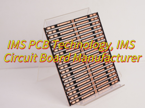
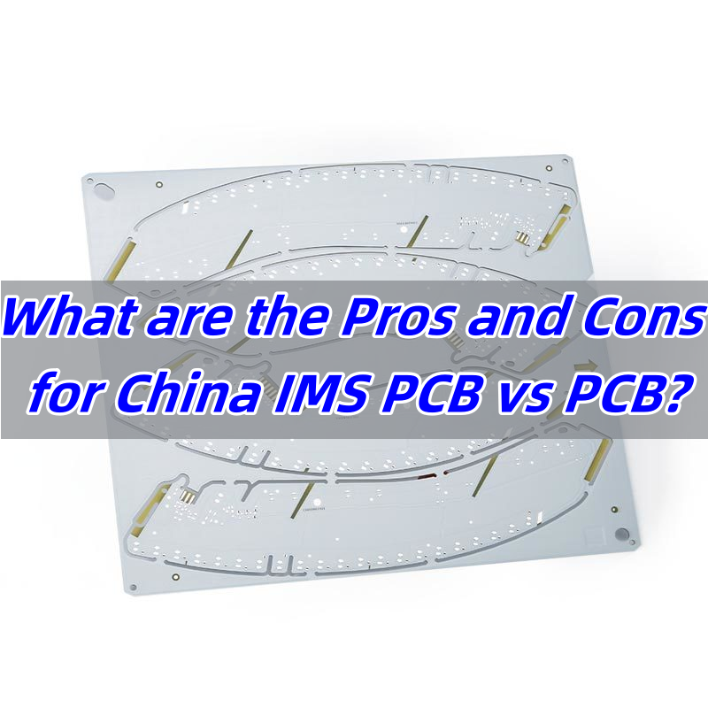
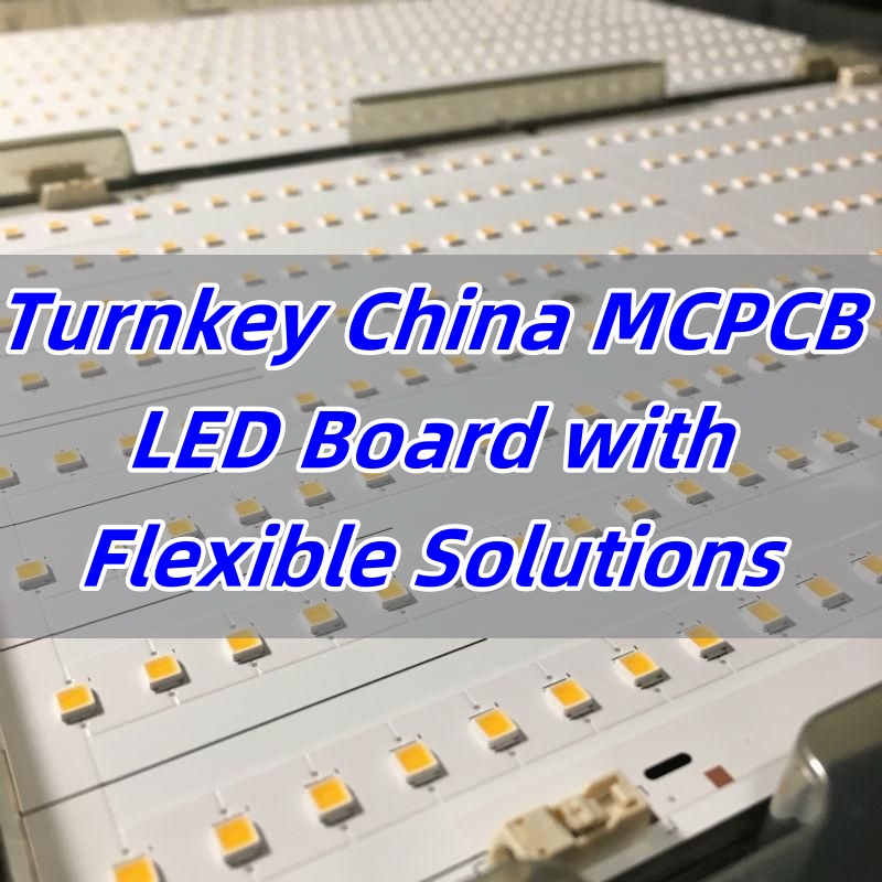
Why choose copper IMS PCB? This guide covers copper IMS PCB from design to manufacturing, highlighting superior heat dissipation, design guidelines for high-power applications, and EBest Circuit (Best Technology)’s precision production capabilities.
Are you bothered by these problems?
- How to break through the heat dissipation bottleneck?
- How to balance cost and performance?
- How to ensure signal integrity?
EBest Circuit (Best Technology) can provide:
- Three-dimensional heat dissipation architecture: Exclusive copper-based composite design, thermal resistance reduced by 40%, achieving a 25°C reduction in temperature rise at the same power consumption.
- Optimized material cost performance: Patented copper-aluminum hybrid process, reducing material costs by 18% while maintaining thermal conductivity.
- Electromagnetic compatibility integration: Built-in gradient impedance design, 5G band signal attenuation is controlled within 0.3dB.
Welcome to contact us if you have any inquiry for metal core PCB: sales@bestpcbs.com.
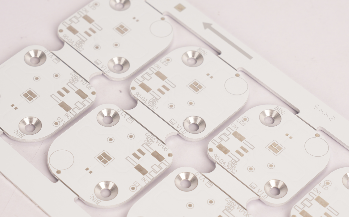
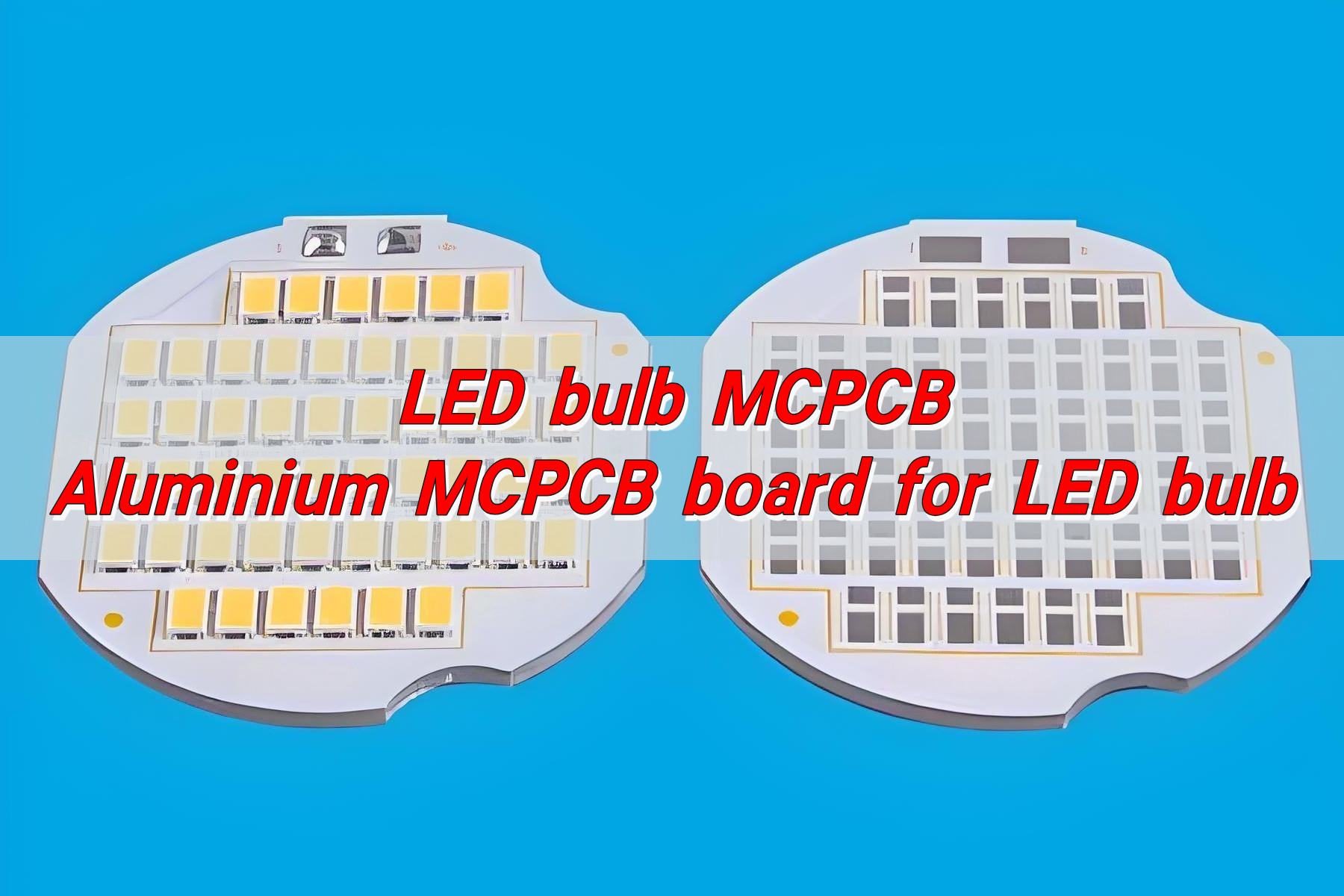
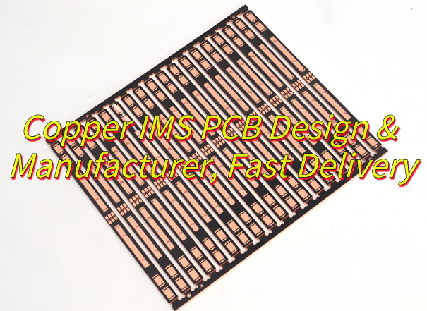
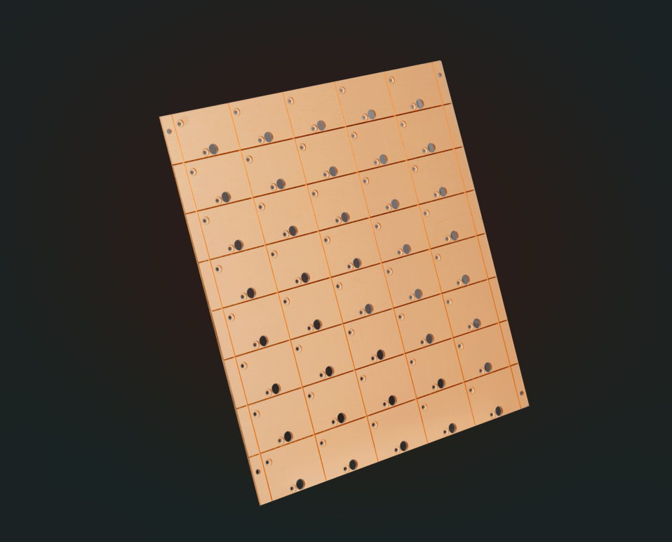
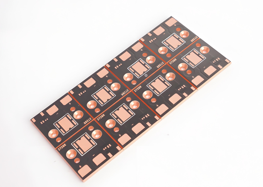
What Is Copper IMS PCB?
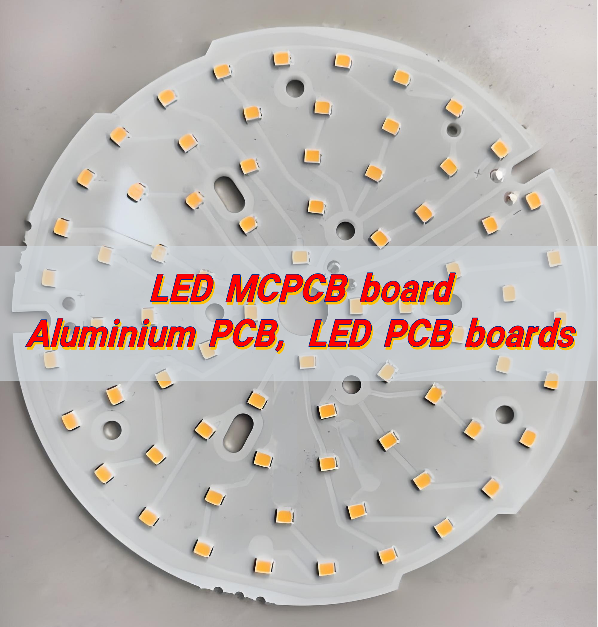
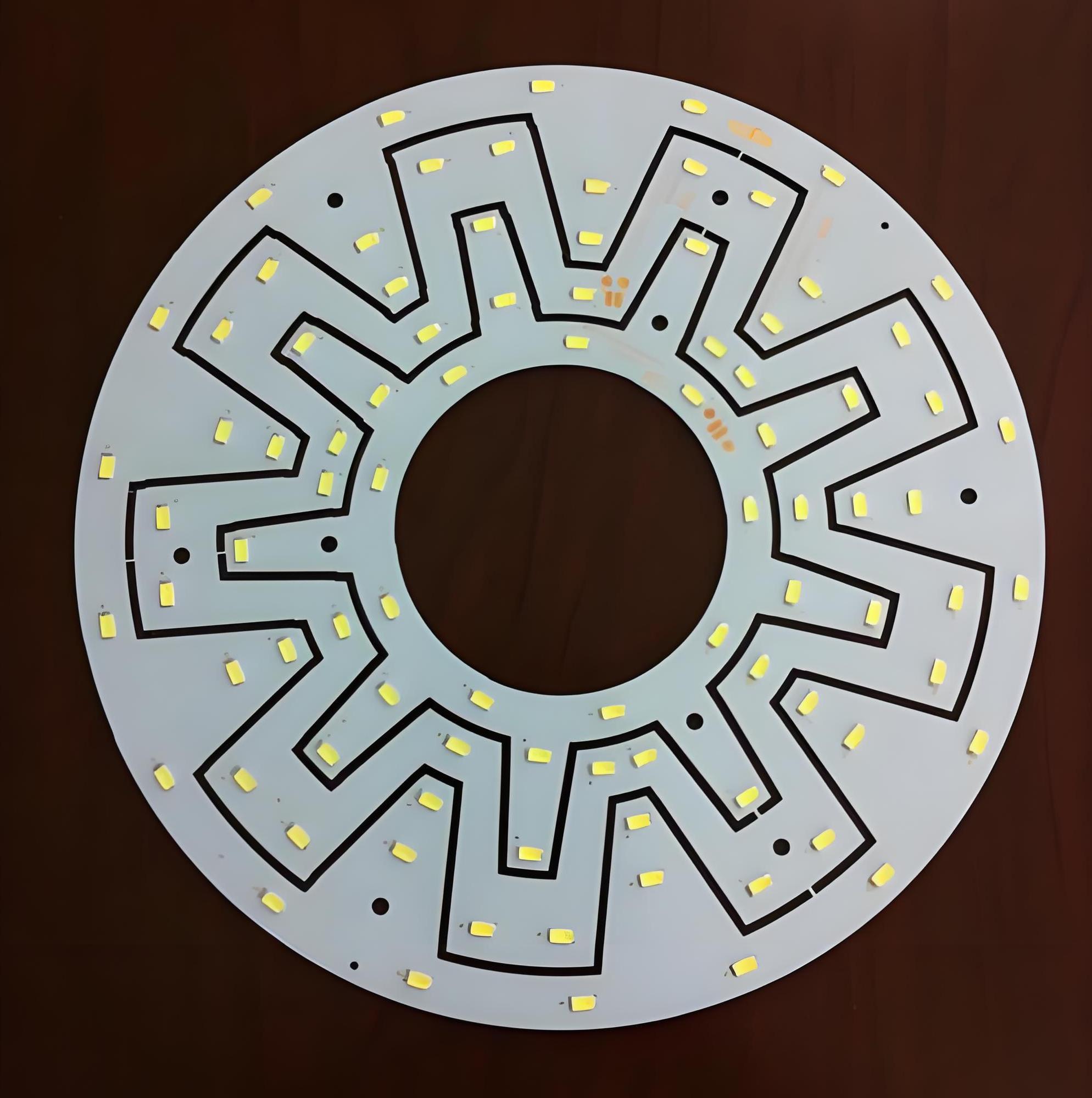
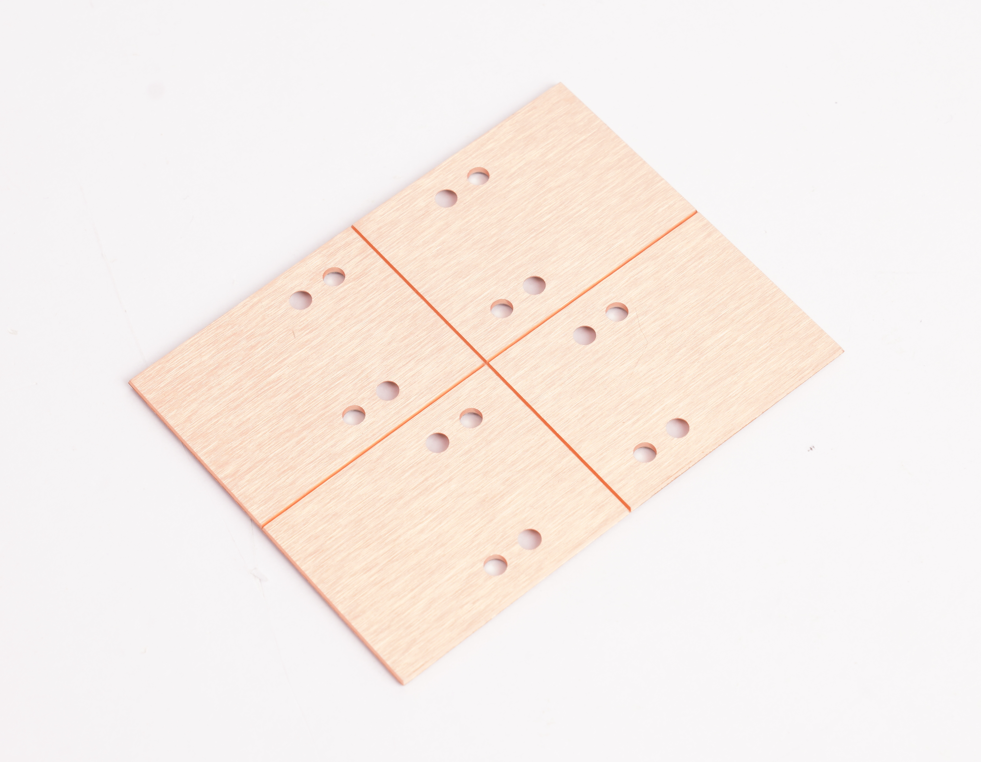
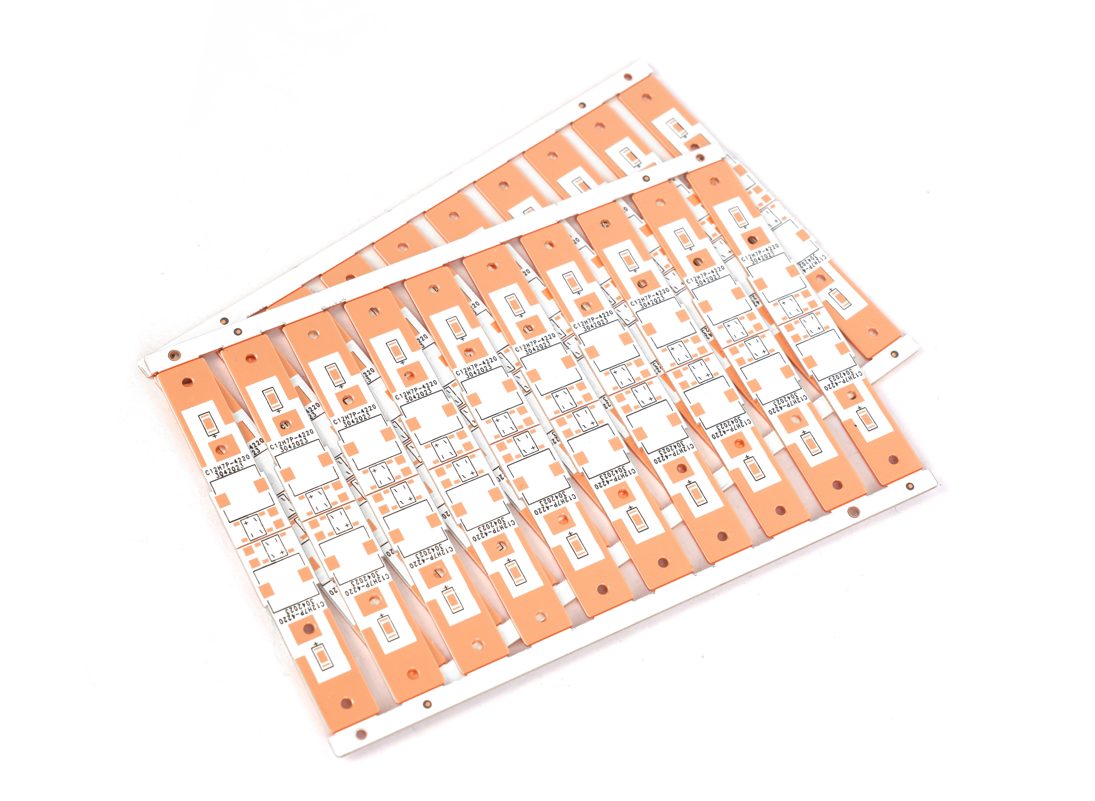
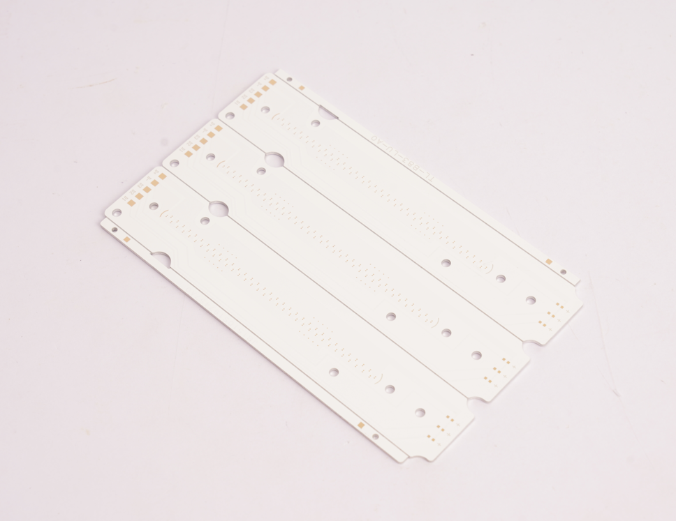
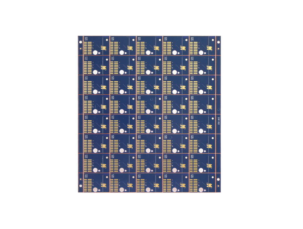
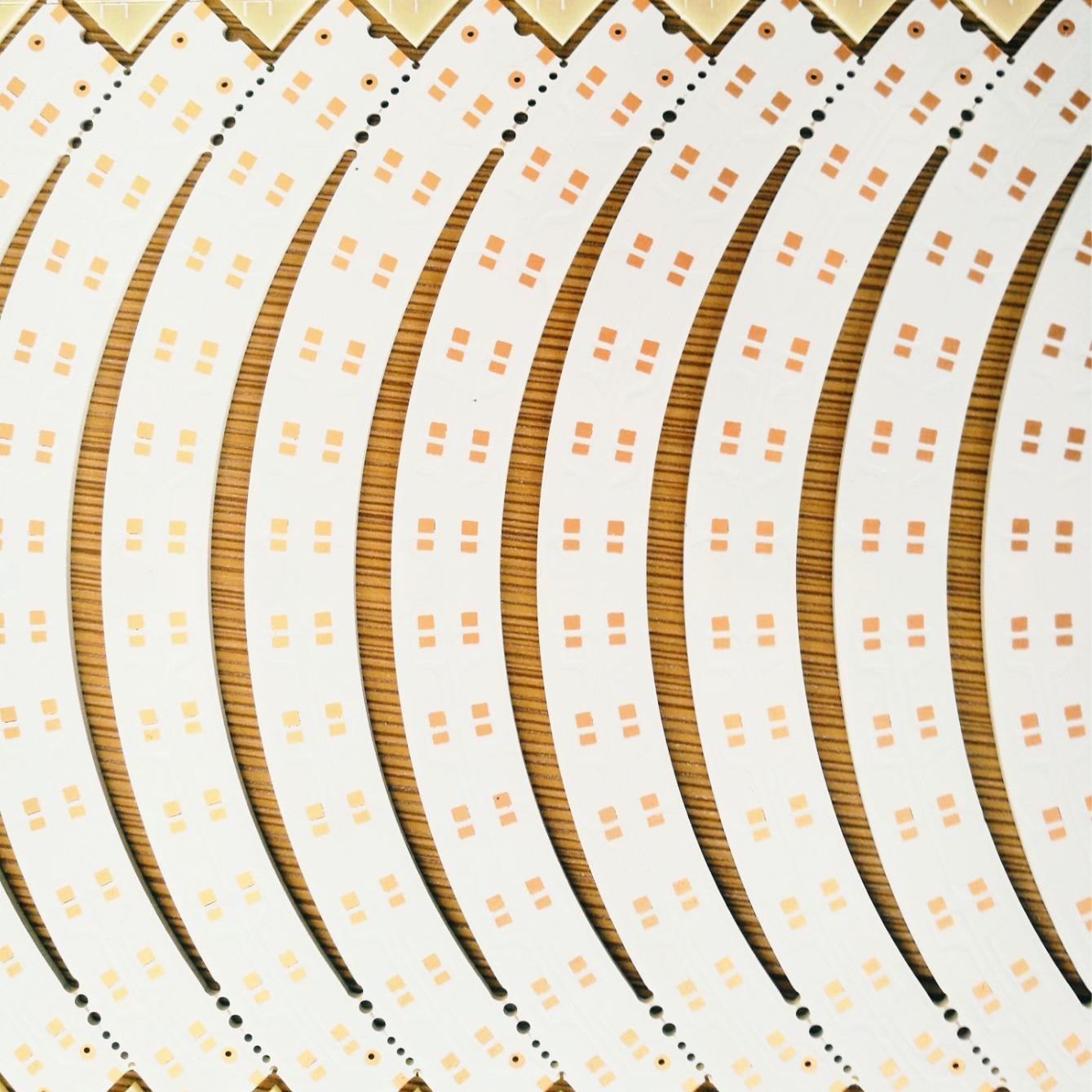
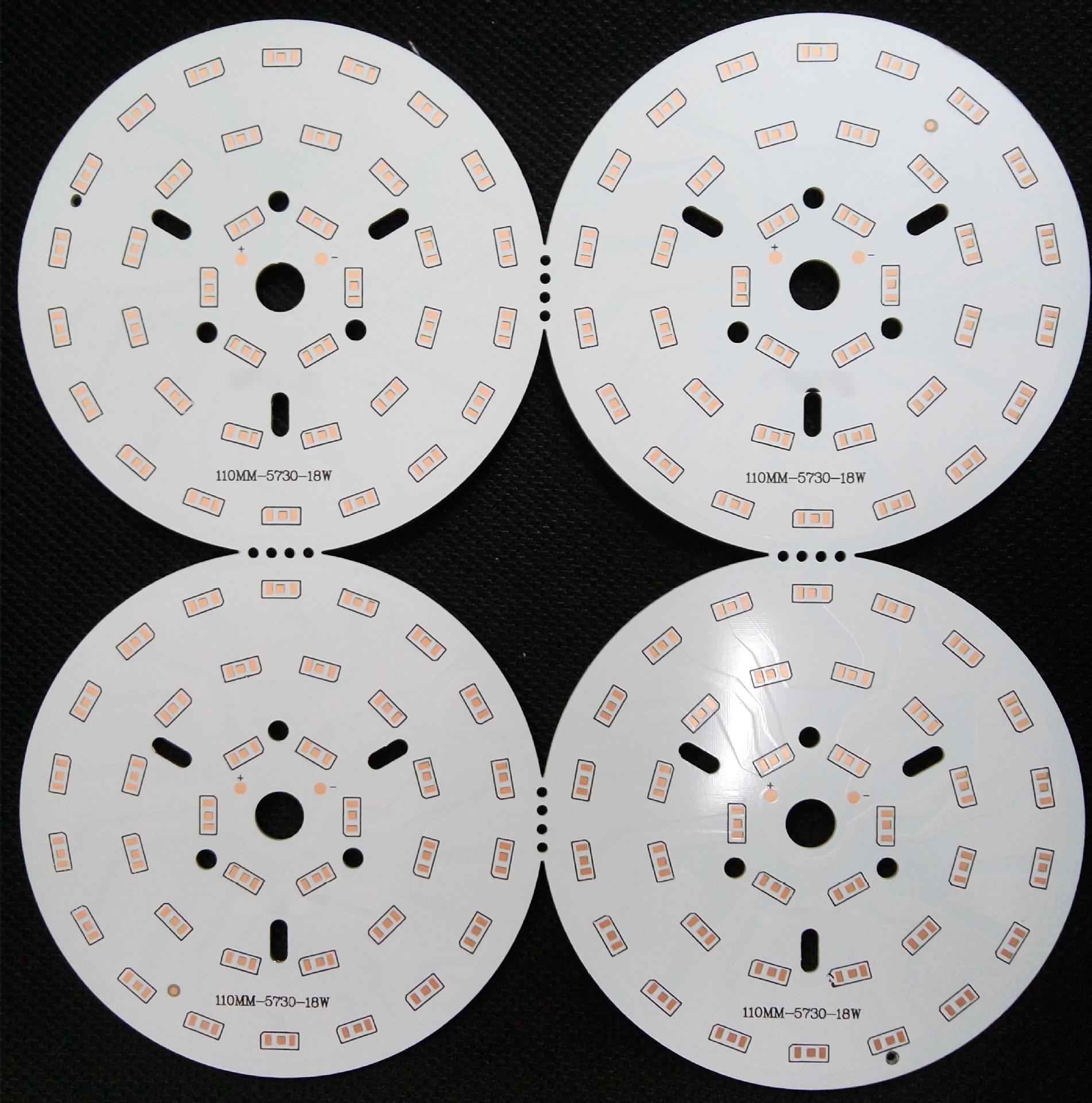
Copper IMS PCB (Insulated Metal Substrate Printed Circuit Board) is a high-performance circuit substrate constructed on a metal base (typically copper or aluminum) coated with a thermally conductive dielectric layer. It combines a copper circuit layer, a ceramic/polymer-based insulating layer, and a metal core to achieve exceptional thermal management (1-12 W/m/K conductivity), electrical insulation, and mechanical stability. Primarily used in high-power applications like LED lighting, automotive power modules, and aerospace systems, it offers 100x lower thermal resistance than FR4 while enabling efficient heat dissipation through its metal core structure.
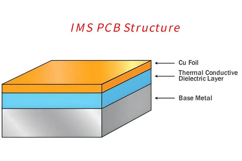
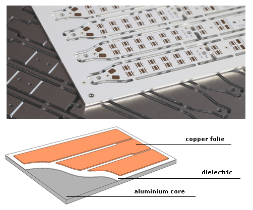
What Is Stackup of Copper IMS PCB?
Copper IMS PCB Stackup Structure
Copper Base Plate
- Material: High-purity electrolytic or rolled annealed copper (1–5 oz thickness) for superior thermal conductivity (398 W/m·K).
- Function: Primary heat dissipation layer, often embedded with thermal vias to enhance heat transfer to external heat sinks.
Dielectric Insulation Layer
- Material: Ceramic-filled epoxy or high-thermal-conductivity prepreg (e.g., 0.15 mm thickness with thermal resistance <0.7°C/W).
- Function: Provides electrical isolation between the copper circuit and base plate while minimizing thermal resistance.
Copper Circuit Layer
- Material: Thin copper foil (0.5–2 oz) for signal/power routing, processed via etching to form circuits.
- Function: Conductive pathways for components, with optimized thickness balancing current capacity and signal integrity.
Solder Mask & Surface Finish (Optional)
- Solder Mask: Protects copper traces and prevents solder bridging.
- Surface Finish: ENIG (Electroless Nickel Immersion Gold) or HASL (Hot Air Solder Leveling) for solderability and oxidation resistance.
Design Considerations
- Symmetry: Mirror-stacked layers (e.g., L1/L4, L2/L3) to prevent warping.
- Thermal Vias: Embedded or plated-through vias to connect heat-generating components to the copper base.
- Material Selection: High-Tg (>170°C) prepreg for stability under thermal cycling.
Copper IMS PCB Specification
| Parameter | Specification |
| Base Material | High-purity copper (C1100/C1020) |
| Thermal Conductivity | 398 W/m·K (pure copper) |
| Dielectric Layer Thickness | 0.1–0.5 mm (ceramic-filled epoxy) |
| Thermal Resistance | <0.7°C/W (0.15 mm dielectric) |
| Max Operating Temp | 150–200°C (depends on dielectric) |
| Copper Thickness | 1–5 oz (35–175 μm) for circuits |
| CTE (Thermal Expansion) | 17 ppm/℃ (matches silicon chips) |
| Dielectric Breakdown | >3 kV (0.1 mm thickness) |
| Solder Mask Options | White/Black (for LED applications) |
What Are Advantages of Copper IMS PCB?
- Ultra-High Thermal Conductivity (398 W/m·K) – Enables 25-40°C lower junction temperatures in high-power devices (e.g., LEDs, IGBTs), extending lifespan by 3-5x.
- Exceptional Current Carrying Capacity (15A/mm²) – Supports 3x higher current density than standard FR4, reducing PCB size by 35% for equivalent power.
- Thermal Expansion Matching (CTE=17ppm/℃) – Eliminates solder joint failures in thermal cycling (-40°C to 150°C), critical for automotive/industrial apps.
- Built-in EMI Shielding – Reduces RF noise by 40dB without additional shielding layers, ideal for 5G/RF circuits.
- High-Frequency Performance – Superior signal integrity for GHz-range applications with minimal signal loss.
- Miniaturization Potential – Supports 0.1mm dielectric layers and microvias for chip-scale packaging in medical/portable devices.
- Long-Term Reliability – Zero oxidation risk and 100% recyclability reduce lifetime costs by 18% vs. aluminum.

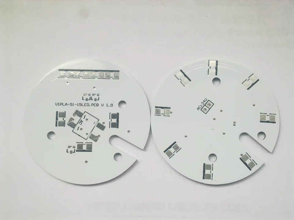
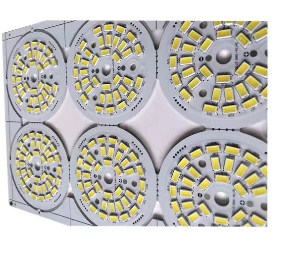
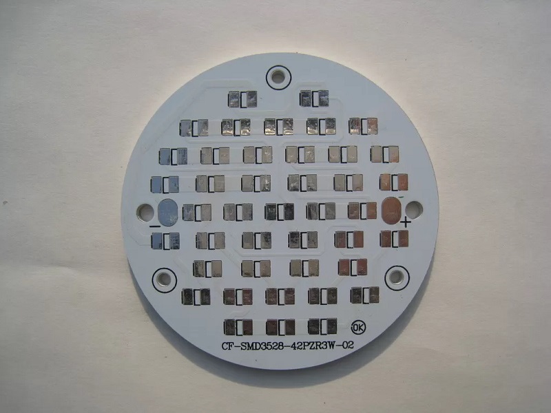
What Are Applications of Copper IMS PCB?
- Automotive: Reduces overheating in LEDs/batteries – longer lifespan, lower maintenance.
- Renewable Energy: Cuts heat loss in solar/wind systems – boosts efficiency, lowers costs.
- Consumer Electronics: Prevents phone/tablet overheating – reliable performance, fewer repairs.
- Medical Devices: Stable operation in critical tools – safer use, fewer replacements.
- Aerospace/Defense: Withstands extreme temps/vibrations – reliable in harsh conditions.
- Industrial Systems: Resists heat deformation – less downtime, higher productivity.
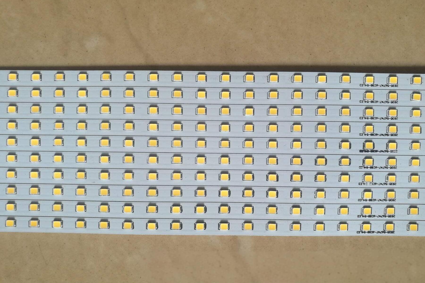
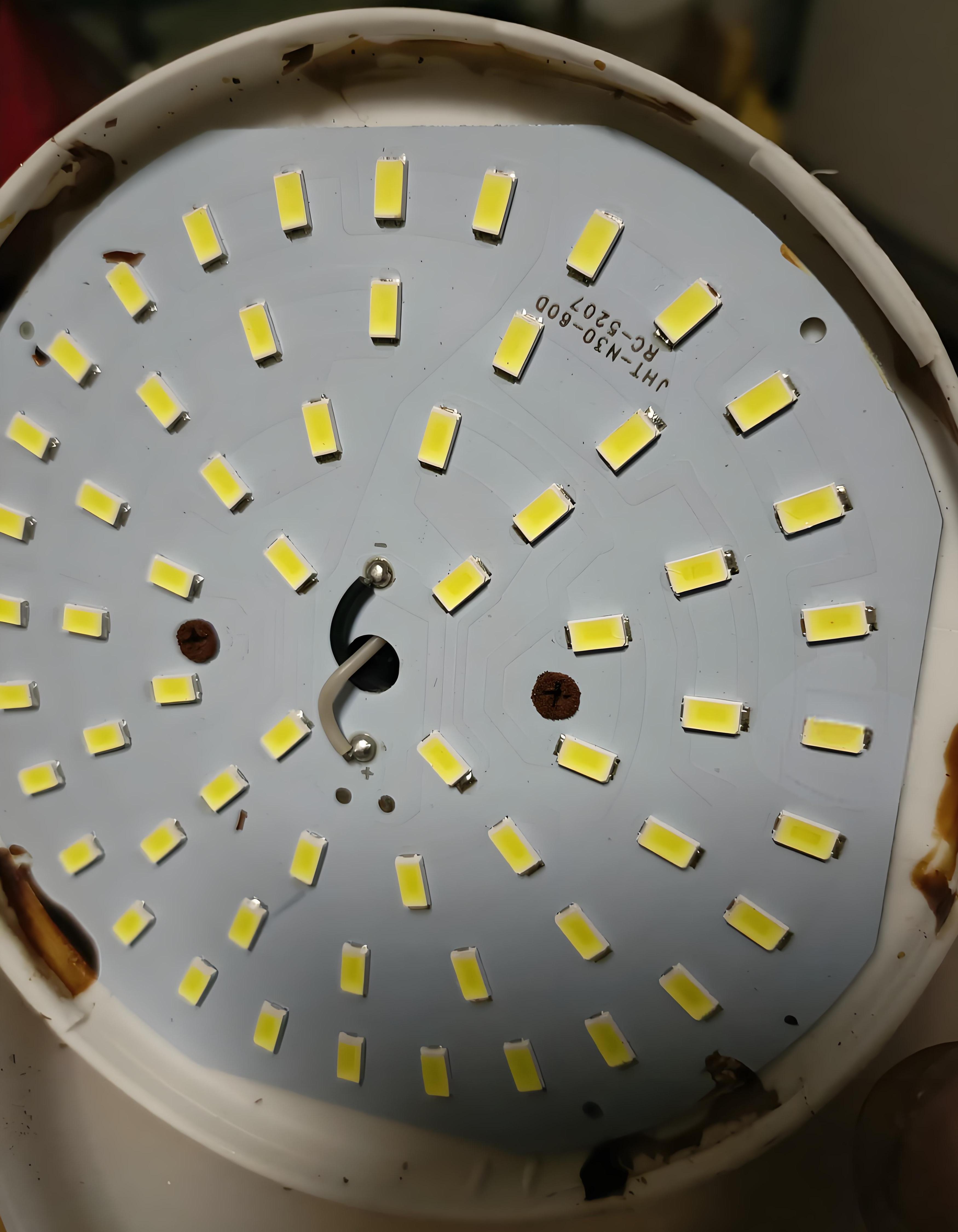
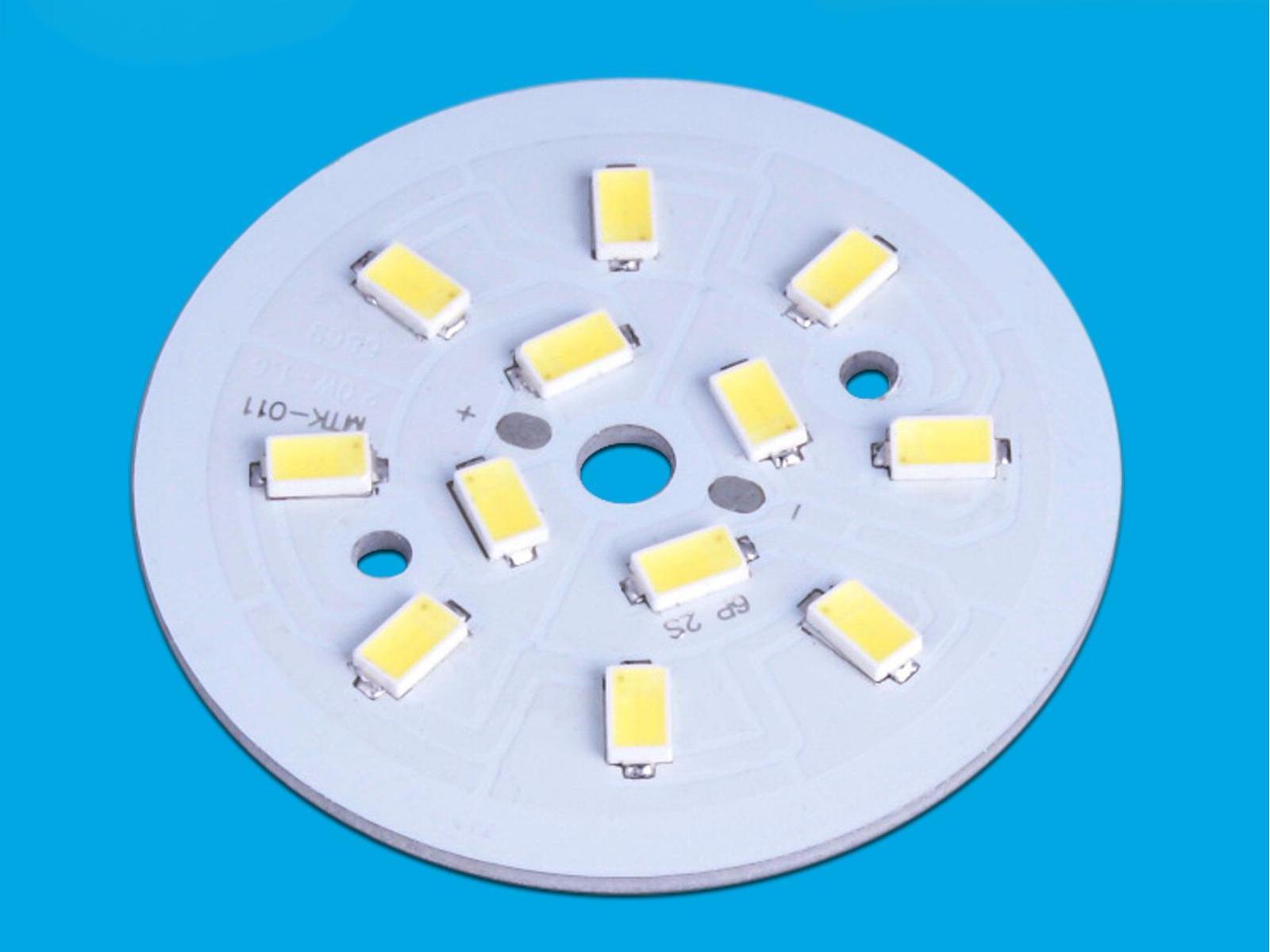
- LED Lighting: Lowers temps in high-power lights – doubles lifespan, saves replacement costs.
How to Design A Copper IMS PCB for High Power?
Design Guidelines for High-Power Copper IMS PCBs
1. Material Selection
- Use thick copper foil (2oz/3oz or higher) to handle high current densities.
- Prioritize low-thermal-resistance dielectric layers (e.g., ceramic-filled polymers) to maximize heat transfer to the copper base.
2. Thermal Management
- Place heat-generating components (e.g., MOSFETs, LEDs) directly over the copper base for direct heat dissipation.
- Add thermal vias under hot components to channel heat vertically to the copper layer.
- Avoid thermal isolation; ensure continuous copper paths for heat flow.
3. Current Path Optimization
- Design wide, short traces for high-current paths to minimize resistance and I²R losses.
- Use parallel traces or polygon pours to distribute current evenly.
- Avoid sharp bends (≥90°) in high-current traces to reduce inductance and hotspots.
4. Layer Stackup
- Prioritize a 2-layer stack: copper base (bottom), dielectric layer, and copper top layer.
- For complex designs, add internal copper layers with prepreg insulation, ensuring thermal vias connect all layers.
5. Mechanical Stability
- Maintain symmetry in layer stackup to reduce warping during reflow.
- Use heavy copper (≥3oz) for rigid base support; avoid over-etching thin features.
6. Component Placement
- Isolate high-power components from sensitive analog/digital sections to prevent thermal interference.
- Leave spacing around heat sinks or mounting holes for airflow or mechanical fixation.
7. Testing & Validation
- Perform thermal simulation (e.g., ANSYS Icepak) to verify heat dissipation under max load.
- Test under worst-case power conditions to ensure junction temps stay below component limits.
Notes: Balance thermal performance, electrical efficiency, and mechanical reliability. Prioritize direct heat paths, robust current handling, and material durability for high-power resilience.
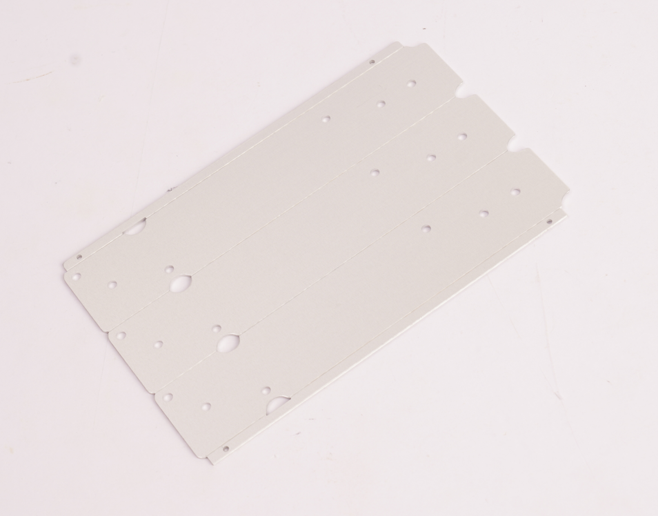
Copper IMS PCB Manufacturing Processes
1. Material Preparation: Start with a copper base plate, a thermally conductive dielectric layer (e.g., ceramic-filled polymer), and top-layer copper foil. Materials are selected for thermal performance and durability.
2. Lamination: Bond the layers under controlled heat and pressure. The copper base, dielectric, and top foil are fused to create a rigid, thermally efficient structure.
3. Drilling: Precision-drill vias and through-holes. Clean debris thoroughly to ensure clean plating surfaces.
4. Plating: Apply electroless or electrolytic copper plating to coat hole walls, enabling vertical electrical connections between layers.
5. Etching: Use photoresist and chemical etching to remove excess copper from the top layer, leaving defined circuit traces.
6. Surface Finish: Apply finishes like ENIG, OSP, or immersion silver to protect exposed copper and enhance solderability during assembly.
7. Cutting & Profiling: Cut the panel into individual PCBs. Machine edges (e.g., V-score, routing) to meet required dimensions and shapes.
8. Quality Testing: Perform electrical tests (continuity, isolation), thermal stress tests (e.g., reflow cycles), and visual inspections to ensure reliability and performance.
Why Choose EBest Circuit (Best Technology) as Copper IMS PCB Manufacturer?
Reasons why choose EBest Circuit (Best Technology) as your copper IMS PCB manufacturer:
- Superior Thermal Performance: Copper core delivers 398 W/m·K conductivity, reducing device temperatures by 30% for extended product lifespan.
- Rapid Prototyping Service: 24-hour turnaround for samples with same-day engineering review.
- Competitive Pricing Structure: Transparent pricing with no hidden fees—cost-effective for high-volume production.
- Strict Quality Control: 100% automated optical inspection (AOI) and X-ray testing for defect-free PCBs.
- Fast Production Lead Times: 15-day standard lead time with expedited options for urgent orders.
- High Current Carrying Capacity: Supports 15A/mm² current density, enabling compact, high-power designs.
- EMI Shielding Built-In: Copper substrate naturally reduces RF noise by 30dB without added layers.
- Precision Laser Drilling: 50μm microvias for ultra-dense interconnects in advanced packaging.
- Custom Material Solutions: Tailored dielectric formulations for specific thermal/electrical requirements.
- Dedicated Engineering Support: 24/7 technical team for design optimization and troubleshooting.
Our Copper IMS PCB Manufacturing Capabilities
| Base material: | Copper |
| Thermal Conductivity (dielectric layer): | 0.8, 1.0, 1.5, 2.0, 3.0 W/m.K. |
| Board Thickness: | 0.5mm~3.0mm(0.02″~0.12″) |
| Copper thickness: | 0.5 OZ, 1.0 OZ, 2.0 OZ, 3.0 OZ, up to 10 OZ |
| Outline: | Routing, punching, V-Cut |
| Soldermask: | White/Black/Blue/Green/Red Oil |
| Legend/Silkscreen Color: | Black/White |
| Surface finishing: | Immersion Gold, HASL, OSP |
| Max Panel size: | 600*500mm (23.62″*19.68″) |
| Packing: | Vacuum/Plastic bag |
| Samples L/T: | 4~6 Days |
| MP L/T: | 5~7 Days |
Our IMS PCB Quality Inspection
1. Electrical Continuity & Isolation Testing
- Method: Automated flying probe/bed-of-nails testing.
- Focus: Verify zero shorts/opens in circuits; ensure ≥50MΩ isolation resistance between traces.
- Purpose: Guarantees functional reliability for high-power signals.
2. Thermal Performance Validation
- Method: Thermal imaging under max load (e.g., 150°C junction temp).
- Focus: Measure thermal resistance (<2°C/W) and hotspot uniformity.
- Purpose: Confirms heat dissipation efficiency for demanding applications.
3. Mechanical Stress Resistance
- Method: 3-point bend test (≥10N force) and vibration testing (20–2000Hz).
- Focus: Ensure <0.2mm warpage and no delamination after stress.
- Purpose: Validates durability in high-vibration environments (e.g., automotive/aerospace).
4. Thermal Cycling Reliability
- Method: -40°C to +150°C cycles (100x).
- Focus: Check for cracks, delamination, or electrical drift post-cycling.
- Purpose: Proves long-term reliability in extreme temperature swings.
5. Solderability & Surface Finish Integrity
- Method: Wetting balance test (ENIG/OSP finishes).
- Focus: Ensure >95% solder coverage with no voids.
- Purpose: Prevents assembly defects and ensures strong component bonds.
6. Dielectric Breakdown Testing
- Method: 500V AC withstand test for 1 minute.
- Focus: Confirm dielectric layer resistance (>1000V) to prevent leakage.
- Purpose: Critical for high-voltage applications (e.g., industrial power systems).
7. Visual & Dimensional Accuracy
- Method: AOI (Automated Optical Inspection) + 2D/3D metrology.
- Focus: Detect micro-cracks, trace misalignment (<50µm tolerance), and pad integrity.
- Purpose: Ensures precision for fine-pitch components (e.g., 0.4mm BGA).
8. Traceability & Certification
- Method: Batch-specific QR codes linked to raw material certs (e.g., UL, RoHS).
- Focus: Full audit trail from copper sourcing to final test data.
- Purpose: Builds trust through transparency and compliance.
How to Get A Quote For Your IMS PCB Project?
How to Get a Quote for Your IMS PCB Project: A Clear Checklist
1. Technical Specifications
- Gerber Files (RS-274X format preferred.
- Bill of Materials (BOM) – Including all components and their specifications.
- Assembly Drawings (if applicable).
- Layer Stackup Details (e.g., dielectric thickness, copper weight).
2. Design Requirements
- Board Dimensions (maximum length, width, and thickness).
- Material Specification (e.g., Copper IMS, aluminum IMS, hybrid options).
- Thermal Requirements (expected operating temperature range).
- Surface Finish (ENIG, HASL, immersion silver, etc.).
3. Quantity & Lead Time
- Order Quantity (low-volume prototypes vs. mass production)
- Desired Lead Time (standard vs. expedited options)
4. Compliance & Certifications
- Industry-Specific Standards (IPC Class 2/3, UL, RoHS, REACH, etc.)
- Testing Requirements (thermal cycling, high-voltage testing, etc.)
5. Packaging & Shipping
- Special Handling Instructions (ESD-safe, vacuum-sealed, etc.)
- Shipping Address & Contact Details.
Next Steps
- Gather all required documents using this checklist.
- Submit your request via email (sales@besttech.com) or our online quote form.
- Receive a detailed quote with timeline, pricing, and DFM recommendations.
Contact us now if you have any request for IMS PCB: sales@bestpcbs.com.