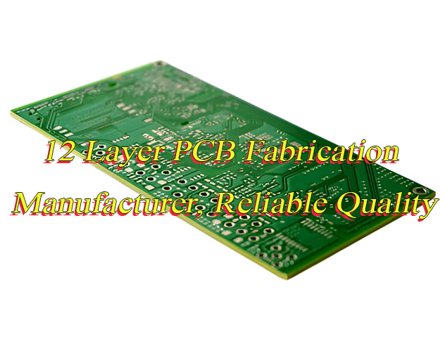
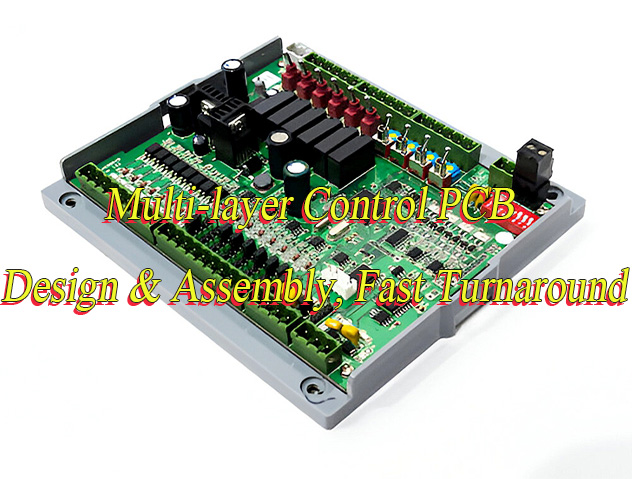
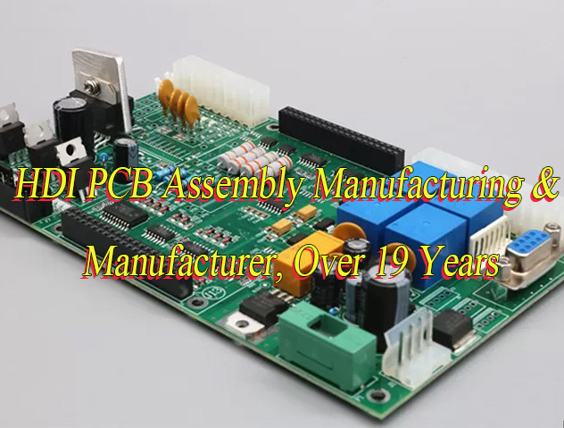
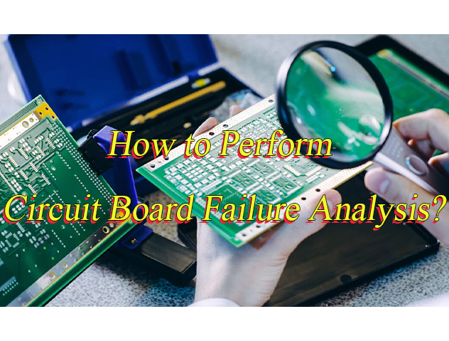
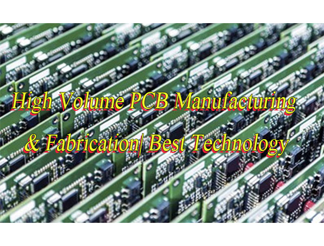
What is high volume PCB manufacturing? Let’s discover features, benefits, application, technical parameter, production process of high volume PCB fabrication.
Are you troubled with these problems?
- How to ensure consistent PCB quality in high-volume orders and avoid batch differences?
- Can existing capacity quickly respond to sudden order surges without delaying product launch timelines?
- How to control yield and cost during mass production of PCBs with complex designs like HDI and high-frequency materials?
As a high volume PCB manufacturer, EBest Circuit (Best Technology) can provide you service and solutions:
- Full-Process Automated Production + Intelligent Quality Control: From drilling to testing, fully automated equipment combined with AI quality inspection systems ensures consistent performance of each PCB, with delivery yield exceeding industry standards.
- Flexible Capacity & Rapid Delivery System: Flexible production line layout + intelligent production scheduling system supports flexible allocation of millions of monthly orders, reducing emergency order production cycles by 30%.
- DFM Optimization & Cost Collaborative Design: Experienced engineer teams intervene in the design phase, reducing material waste through process optimization, lowering mass production costs for complex structures by 15%-20%.
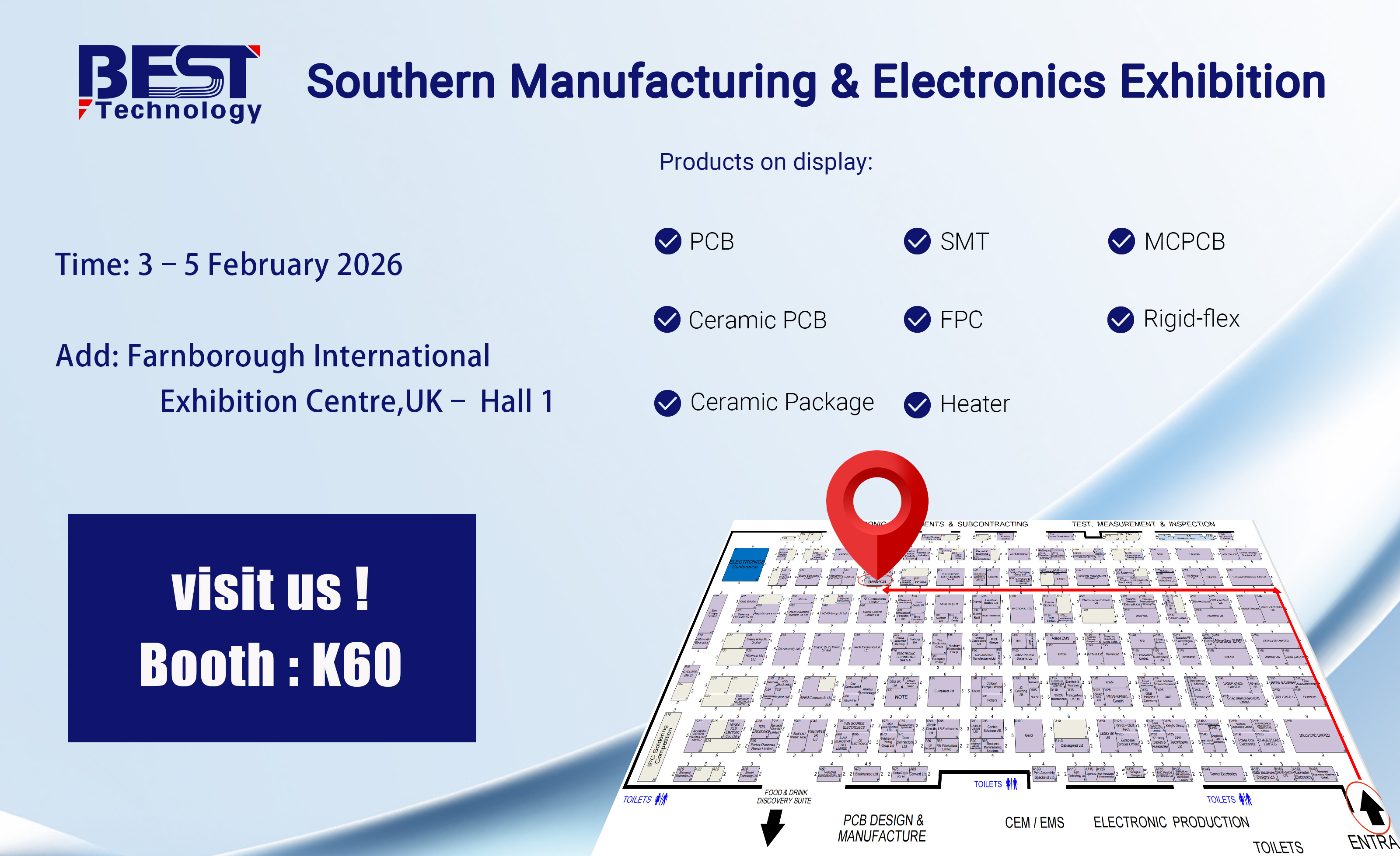
Welcome to contact us if you have any inquiry for high volume PCB fabrication: sales@bestpcbs.com.
What Is High Volume PCB Manufacturing?
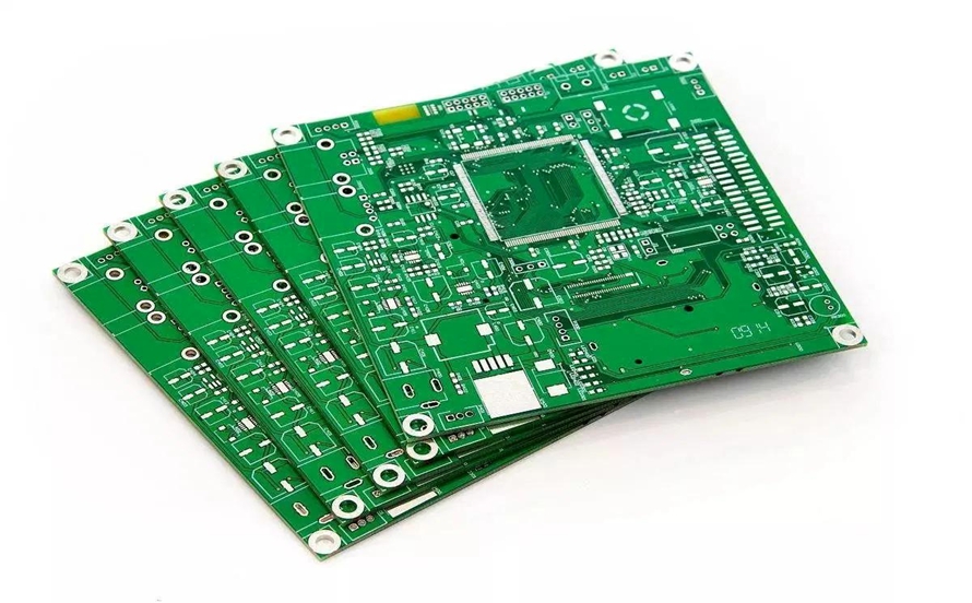
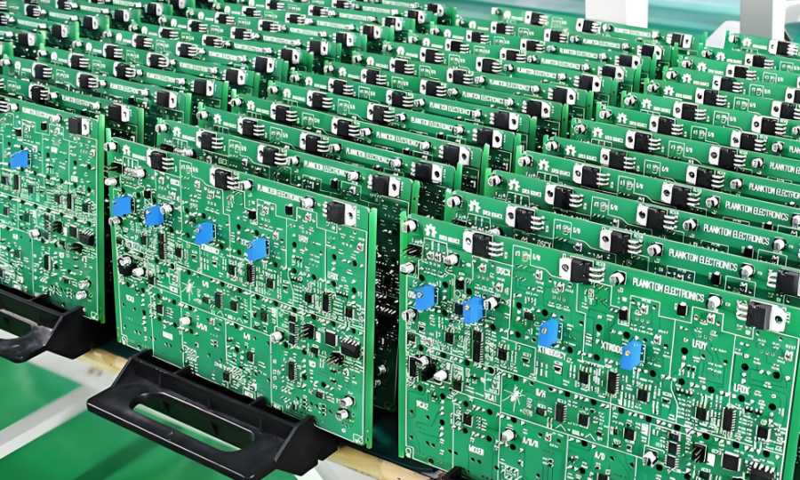
High volume PCB manufacturing refers to a manufacturing process specifically designed and optimized for producing extremely large quantities of printed circuit boards, typically involving single-order volumes of thousands to tens of thousands of units. Its core features include highly automated production lines, standardized process workflows, scaled raw material procurement, and rigorous process control. These elements work together to minimize per-unit costs, maximize production efficiency, and ensure high consistency in quality stability. This model is well-suited for products with stable and massive demand, such as consumer electronics, automotive electronics, and industrial equipment.
Feature of High Volume PCB Fabrication
- Economies of Scale: By producing in massive quantities, fixed costs such as tooling fees, equipment depreciation, and engineering setup costs are spread across units, significantly reducing per-PCB cost.
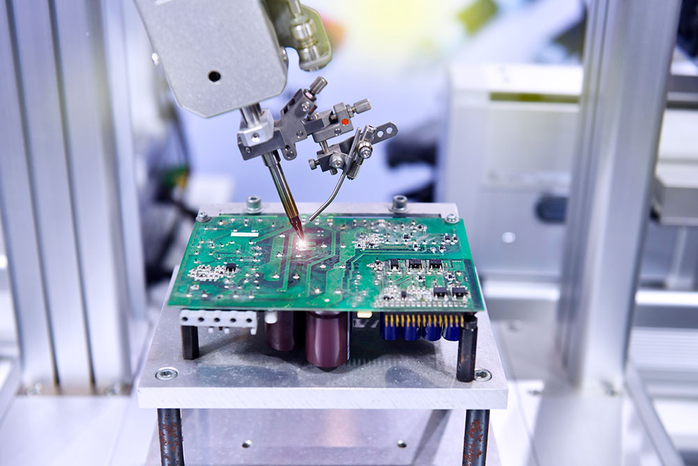
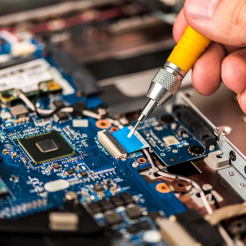
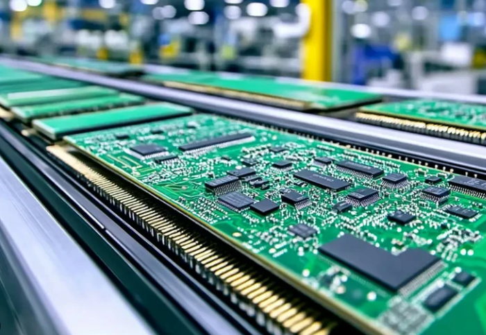
- High Automation: From material handling, imaging transfer, etching, drilling, plating, solder mask/silkscreen printing, surface finishing to testing, depaneling, and packaging, automated equipment and assembly lines are extensively used to maximize efficiency and consistency while minimizing human intervention.
- Process Optimization: Production workflows are meticulously designed and continuously refined to minimize bottlenecks, waiting times, and waste, enabling smooth, assembly-line operations.
- Standardization and Consistency: Emphasis on standardized operations and stringent quality control systems ensures PCBs produced across different batches or time periods maintain high consistency and reliability in electrical performance and appearance.
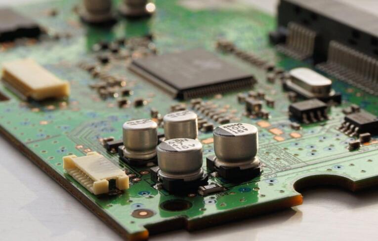
- Specialized Equipment and Tooling: Heavy investment in high-speed, high-precision, durable equipment, such as high-throughput drilling machines, VCP vertical continuous plating lines, AOI automatic optical inspection systems, flying probe/bed-of-nails testers, and high-speed SMT lines, along with long-life stencils and test fixtures.
- Supply Chain Integration: Requires a robust and reliable raw material supply chain for components like copper-clad laminates, copper foils, chemicals, and components to ensure sustained, stable large-scale supply.
- Minimized Setup/Changeover Time: Standardized designs, optimized production scheduling, and universal fixtures reduce line changeover times between different orders or designs.
- Data-Driven Decision Making: Real-time monitoring and data analysis via manufacturing execution systems, quality control data, and equipment monitoring systems enable continuous production optimization.
Advantages of High Volume PCB Manufacturing
- Significantly Reduce Per-Unit Costs: Through scale effects, bulk raw material procurement and automated production lines spread fixed costs, sharply lowering average PCB manufacturing costs per unit.
- Boost Production Efficiency and Delivery Speed: Specialized equipment and automated workflows minimize line changeover and tuning time, enabling faster completion of large orders and accelerating time-to-market.
- Enhance Quality Consistency and Reliability: Standardized processes and full-automation inspection systems minimize human error, ensuring uniform electrical performance and appearance across batches.
- Stabilize Supply Chain and Procurement: Long-term, high-volume partnerships secure key component supply, avoid material shortages, and secure more competitive material pricing.
- Support Large-Scale Market Deployment: High-volume manufacturing capacity allows clients to meet massive sales or deployment demands at once, preventing missed market opportunities due to capacity constraints.
- Enable Smooth Transition from Prototype to Mass Production: With the same supplier involved in prototyping, validated processes carry over directly to volume production, reducing re-tuning time and risks.
Applications of High Volume PCB Fabrication
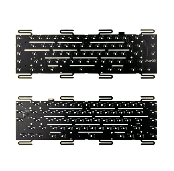
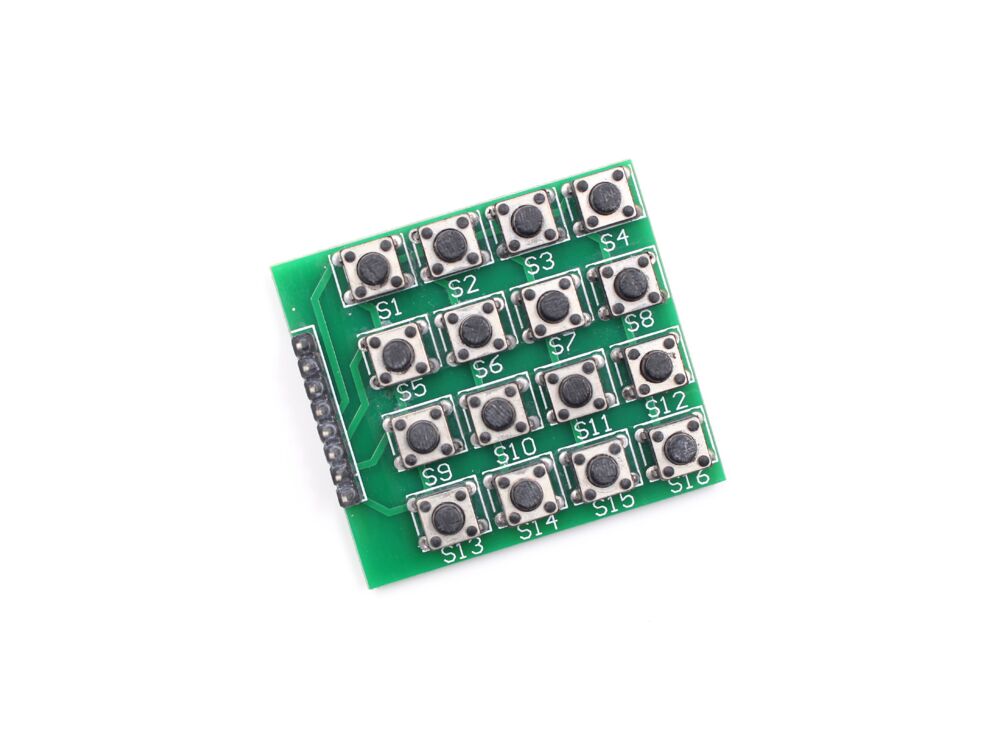
- Consumer Electronics: Mass-produced devices like smartphones, tablets, laptops, wearables, and smart-home products depend on high-volume PCB fabrication to meet global demand while maintaining low per-unit costs.
- Automotive Systems: Modern vehicles integrate PCBs in engine control units (ECUs), infotainment systems, ADAS, and electric vehicle battery management, requiring large-scale production to supply automotive needs.
- Aerospace & Defense: Avionics, navigation, communication, and mission-critical systems in aircraft, satellites, and military equipment use high-volume PCB production for reliability under stringent standards.
- Medical Devices: Diagnostic imaging tools, patient monitors, surgical instruments, and portable medical equipment are produced at scale using PCBs compliant with medical safety and traceability regulations.
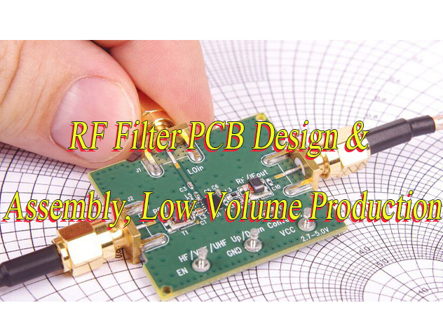
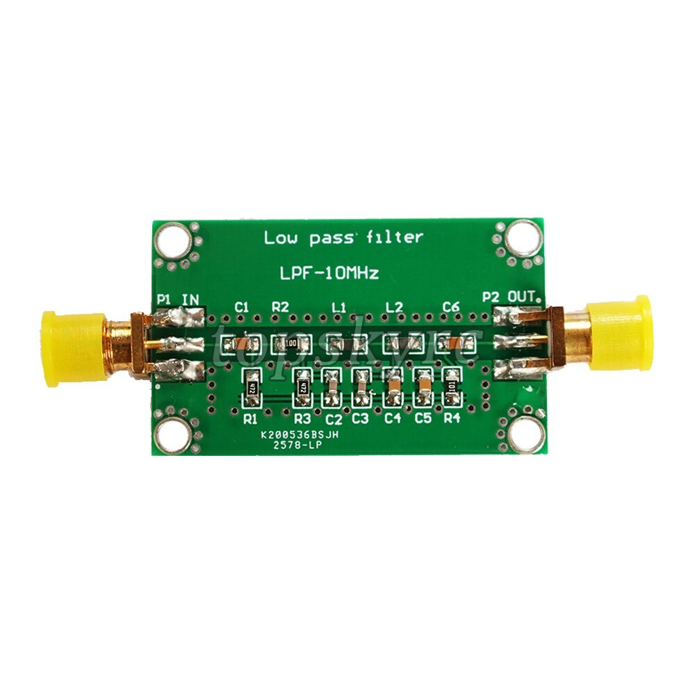
- Telecommunications: 5G infrastructure, base stations, network switches, and routers demand high-volume RF/microwave PCB fabrication to support widespread deployment and high-frequency performance.
- Industrial Electronics: Automation controllers, motor drives, sensors, and power-supply systems utilize high-volume PCBs to endure industrial environments and ensure long-term supply stability.
- Computing & Data Centers: Server motherboards, storage systems, and high-speed networking hardware are manufactured at scale to support cloud and enterprise IT infrastructure growth.
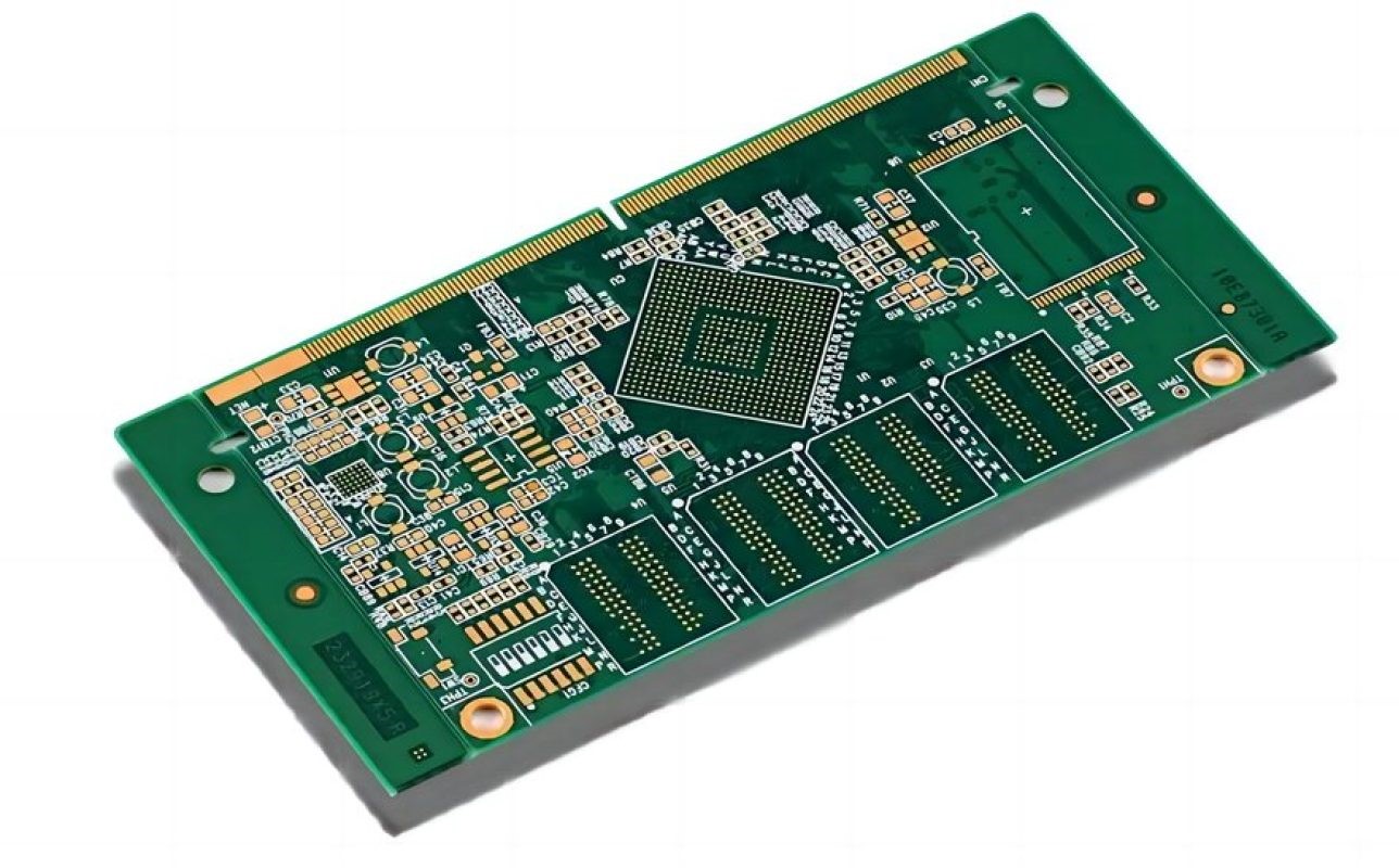
High Volume PCB Manufacturing Technical Requirements
| Technical Indicators | Typical Range/Options |
| Number of Layers | 1–64 layers (standard); HDI up to 20+ layers |
| Material Type | FR-4, FR-4 High-Tg, Polyimide (Flex), Aluminum Substrate, Rogers, Hybrid Materials |
| Maximum Board Size | 500mm × 600mm (standard); 600mm × 1200mm (optional) |
| Board Thickness Range | Rigid: 0.2mm–4.0mm; Flexible: 0.01mm–0.25mm |
| Thickness Tolerance | ±10% |
| Minimum Line Width/Spacing | Standard: 0.10mm/0.10mm; HDI/Fine-Line: 0.035mm/0.035mm |
| Outer Layer Copper Thickness | 1/2oz–6oz (up to 20oz heavy copper) |
| Inner Layer Copper Thickness | 0.5oz–4oz |
| Minimum Mechanical Drill Hole Size | 0.10mm |
| Minimum Laser Drill Hole Size | 0.075mm (HDI) |
| Maximum Aspect Ratio | 15:1 |
| Via Treatment | Through-hole, Blind/Buried Vias, Via-in-Pad, Copper-Filled Vias |
| Common Surface Finishes | HASL (Lead-Free), ENIG, Immersion Tin, OSP, Immersion Silver, Electroplated Gold, etc. |
| Solder Mask Alignment Accuracy | ±0.0375mm |
| Minimum Solder Mask Bridge Width | 0.075mm |
| Silkscreen Line Width | ≥0.10mm (standard) |
| Impedance Control Tolerance | ±10% |
| High-Voltage Testing | 500V–3000V (automated testing) |
| Quality Standards | IPC-A-600 Class 2/3, ISO 9001, IATF 16949, UL, RoHS |
| Minimum Order Quantity | 1 panel (prototype) to 10,000+ panels (volume) |
| Typical Lead Time | 2 days–5 weeks (depending on complexity and quantity) |
High Volume PCB Manufacturing Process
1. Engineering Qualification (EQ)
- Customer-provided design files including Gerber data and drilling data undergo rigorous engineering checks, encompassing Design Rule Check (DRC) validation of line width/spacing and hole position accuracy against manufacturing capabilities, as well as Design for Manufacturing (DFM) analysis to evaluate process feasibility.
- Process specifications such as laminate temperature and drilling parameters are established. For high-density boards, LDI laser direct imaging replaces traditional film methods to ensure ±0.01mm alignment accuracy.
2. Material Preparation and Inner Layer Fabrication
- Substrates are selected from FR-4, high-frequency laminates (e.g., Rogers) or aluminum substrates, with copper foil thickness ranging from 0.5oz to 6oz based on requirements. Inner layer fabrication involves film lamination (70-80°C, 0.3-0.5MPa), exposure (80-120mJ/cm²), development (1%-2% sodium carbonate solution, 25-30°C), and etching (180-220g/L copper chloride solution, 45-50°C) to form circuit patterns. Copper thickness deviation is controlled within ±5%.
3. Inner Layer Oxidation (Brown Oxide)
- Chemical oxidation treatment (5%-10% alkaline solution, 50-60°C) is applied to the inner layer copper surface to generate an oxide layer that enhances bonding strength with resin. Post-drying moisture content must remain below 0.1% to prevent lamination bubbles.
4. Lamination
- Layers are stacked in the design sequence (e.g., Top-bonding sheet-GND layer-bonding sheet-Bottom) with alignment marks deviation ≤0.05mm. Vacuum pressing is performed at 2°C/min heating rate to 180°C, with staged pressure application up to 30kg/cm². A 90-minute dwell period ensures bonding sheet curing degree ≥90%, followed by a 1°C/min cooling rate to avoid interlayer separation.
5. Drilling
- CNC drilling machines (30,000-50,000rpm) or laser drilling systems (CO₂ laser for resin ablation, UV laser for blind holes) create through-holes and blind holes. Aspect ratios are controlled at 10:1 for through-holes and 0.75:1 for micro-holes. Desmear treatment uses potassium permanganate solution (60-80g/L, 70-80°C) for 10-15 minutes, achieving surface roughness Ra≤1.5μm.
6. Hole Metallization
- After desmear treatment, electroless copper deposition (40-50°C, pH 12-13, 20-30 minutes) forms a 1-2μm thin copper layer. Electrolytic copper plating (1-2A/dm² current density, 60-90 minutes) thickens it to target thickness (via copper thickness ≥20μm) with deviation ≤±10%.
7. Outer Layer Image Transfer
- Photoresist is applied to the outer copper surface, exposed, and developed to form circuit patterns. Pattern plating thickens the line copper layer, with line width deviation ≤±0.03mm and burr-free edges.
8. Outer Layer Etching
- Acidic etching solution removes unprotected copper, preserving the plated circuit pattern. Etching rate is 2-3μm/min, ensuring no residual copper and line thinning ≤±0.02mm.
9. Solder Mask and Silkscreen
- Liquid photosensitive solder mask ink (25-30μm thickness) is applied, exposed, and developed to expose pads. Silkscreen printing marks component identifiers and polarity symbols (line width ≥0.10mm), followed by high-temperature curing (150°C, 60 minutes).
10. Surface Finish
- Surface finishes are selected based on requirements: immersion gold (Au thickness 0.1-0.2μm), HASL (Sn-Pb alloy thickness 5-10μm), OSP (organic solderability preservative), or immersion silver (thickness 0.05-0.2μm). Immersion gold suits precision applications (e.g., BGA chips), HASL offers cost efficiency with lower surface flatness, and OSP provides eco-friendly simplicity.
11. Profiling and Outline Processing
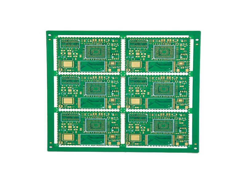
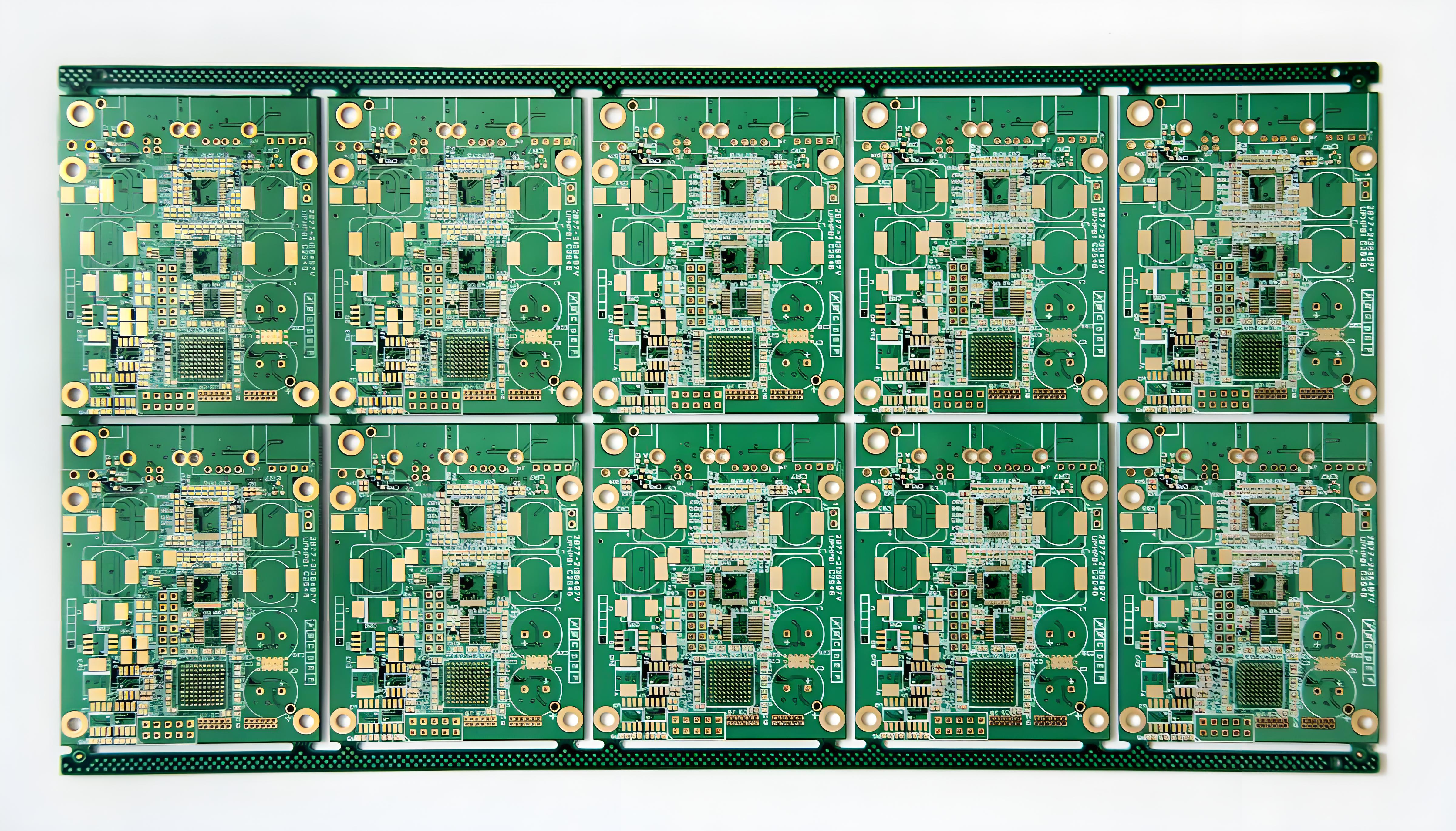
- CNC milling (±0.05mm accuracy), V-cutting, or laser cutting (for irregular shapes) separates large panels into individual PCBs. Edge chamfering, slot machining, and plasma cleaning remove residual adhesive.
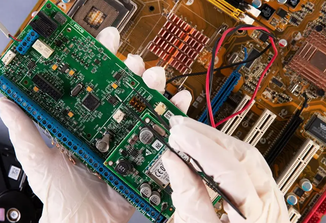
12. Electrical Testing and Inspection
- Flying probe testing (small batches) or bed-of-nails testing (large batches) conducts continuity checks. Automated Optical Inspection (AOI) detects opens/shorts, X-Ray verifies interlayer alignment (deviation ≤0.1mm), and impedance testing validates differential pair tolerance (±10%).
13. Final Inspection and Packaging
- Visual inspection ensures no bubbles or wrinkles, with dimensional verification (total thickness 1.6mm±0.08mm). Certified boards are packaged in anti-static materials (vacuum sealing/moisture barrier bags) for shipment.
Why Choose EBest Circuit (Best Technology) as High Volume PCB Manufacturer?
Reasons why choose us as high volume PCB manufacturer:
- International Certification Credentials: Holding ISO 9001 quality management, ISO 14001 environmental management, UL safety certification, and RoHS compliance certificates, ensuring products meet EU, US, and other global market access standards to facilitate seamless international business expansion.
- Superior Quality Assurance: Utilizing international top-tier substrates and high-precision testing equipment to ensure stable electrical performance, high-temperature/high-humidity resistance, meeting stringent requirements in aerospace, medical, and other critical fields, reducing customer product failure rates and after-sales costs.
- Rapid Delivery Capability: Achieving 7-15 day standard lead times through intelligent production scheduling systems and global logistics networks, with urgent orders deliverable in as fast as 3 days, supporting overseas clients in adjusting production rhythms flexibly to seize market opportunities.
- Cost Optimization Solutions: Leveraging large-scale production and vertically integrated supply chains to offer tiered pricing systems, with batch order prices 10%-20% lower than industry averages, while providing free cost-saving design recommendations for clients.
- Complimentary DFM Design Support: Professional engineering teams deliver end-to-end DFM analysis from stack-up design to impedance matching, identifying manufacturability risks early to minimize trial runs and shorten product launch cycles by over 30%.
- Multilingual Technical Coordination: Providing 24/7 bilingual technical support with dedicated overseas engineer teams for direct client engagement, enabling swift responses to design changes and technical inquiries while eliminating cross-timezone communication barriers.
- Eco-Friendly Process Commitments: Adopting lead-free soldering, wastewater recycling, and other green manufacturing techniques compliant with REACH, SFDR, and other environmental regulations to help clients meet ESG requirements and enhance international brand reputation.
- Long-Term Partnership Guarantees: Establishing strategic collaboration mechanisms with dedicated service teams, priority capacity reservations, and annual quality reviews for long-term clients to continuously reduce total cost of ownership (TCO) through sustained improvement.
Welcome to contact us if you have any inquiry for high volume PCB manufacturing: sales@bestpcbs.com.