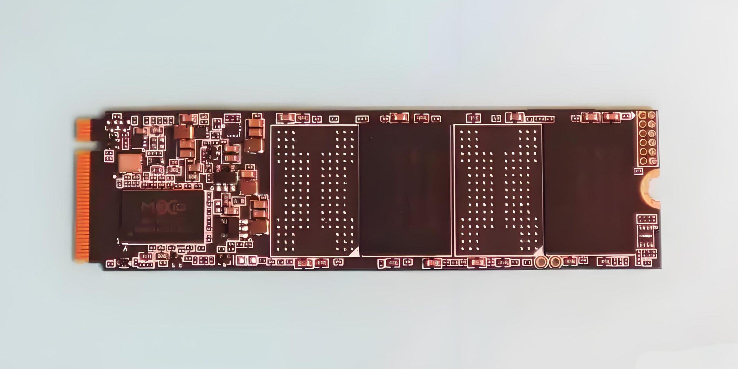
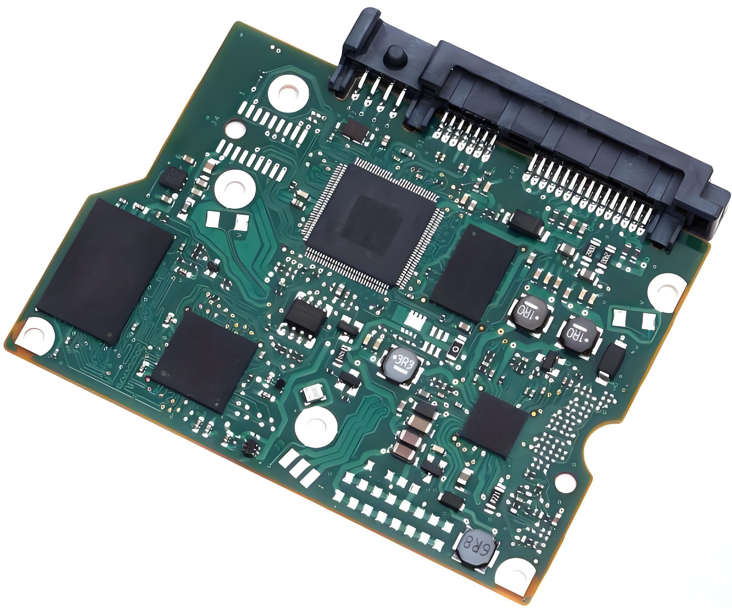
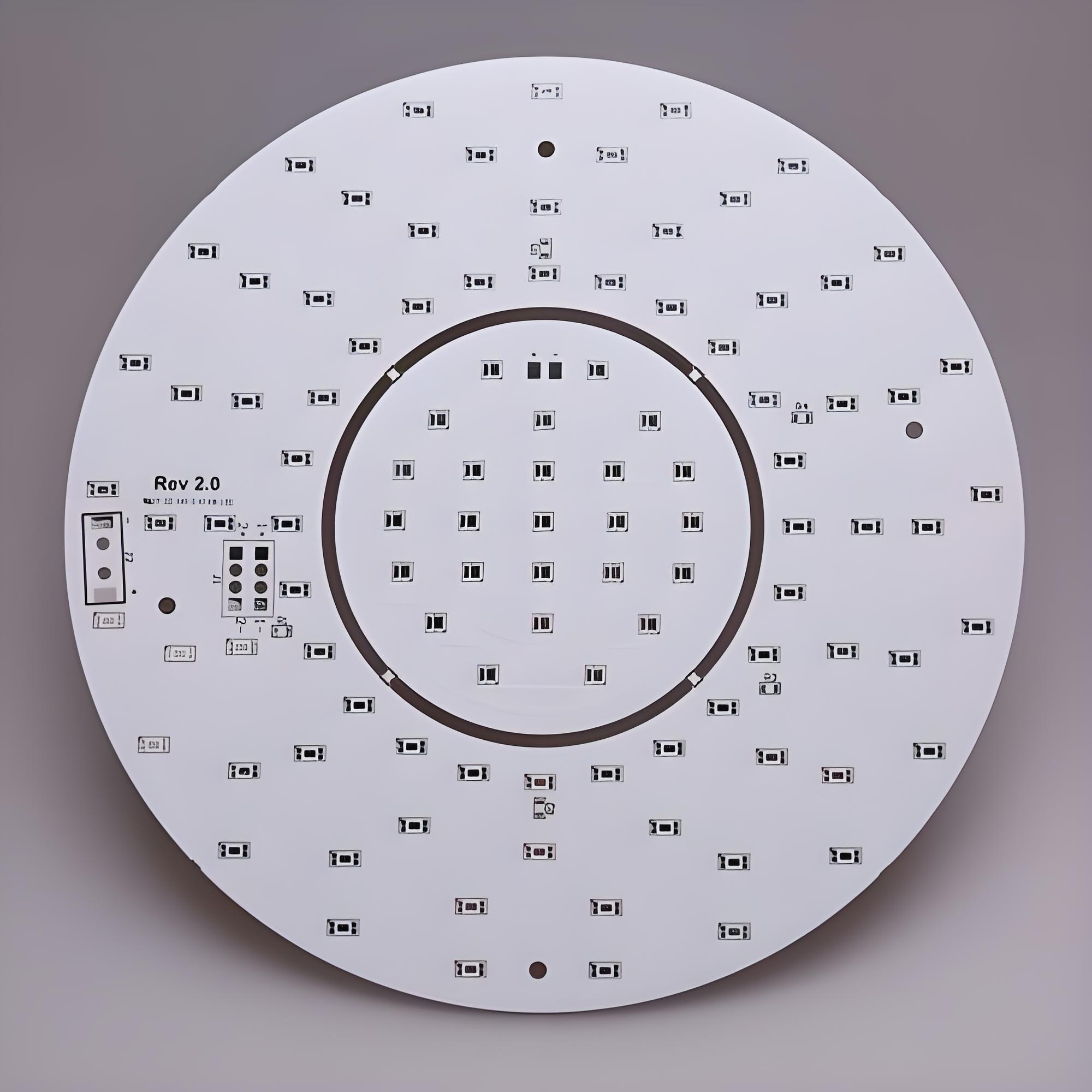
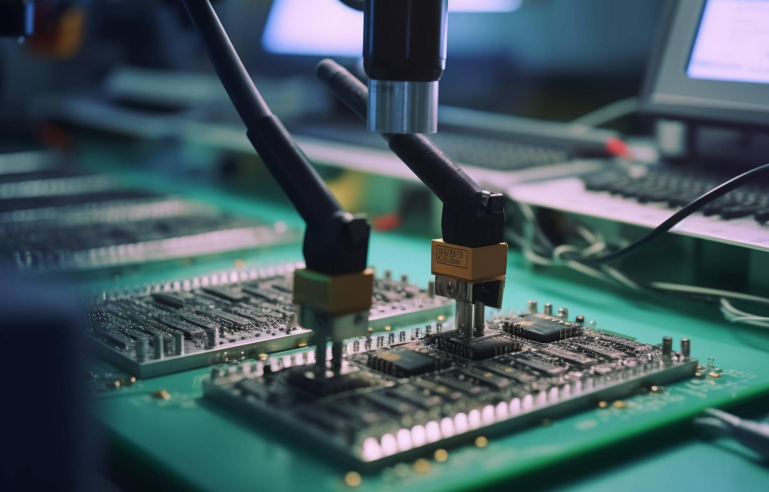
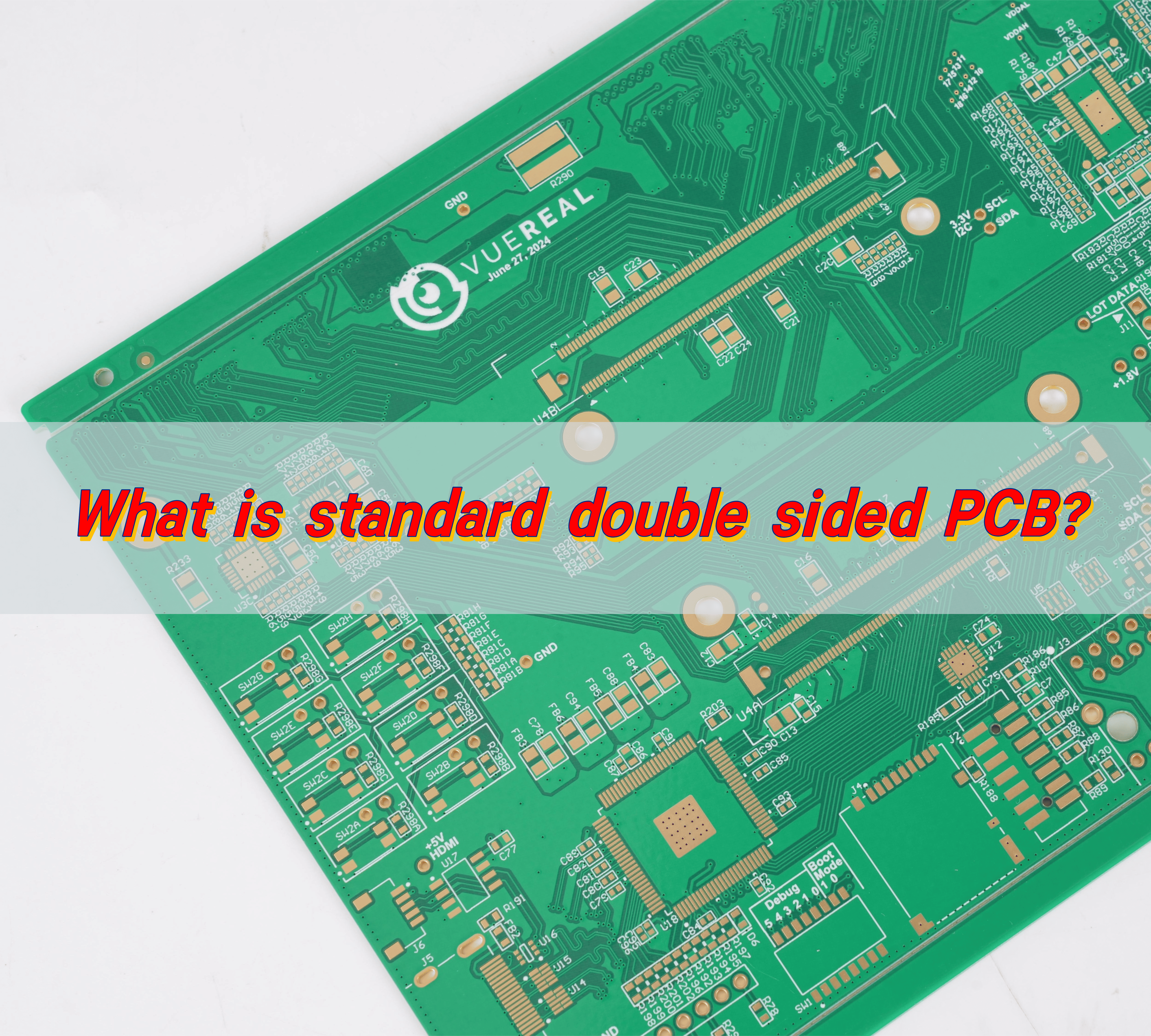
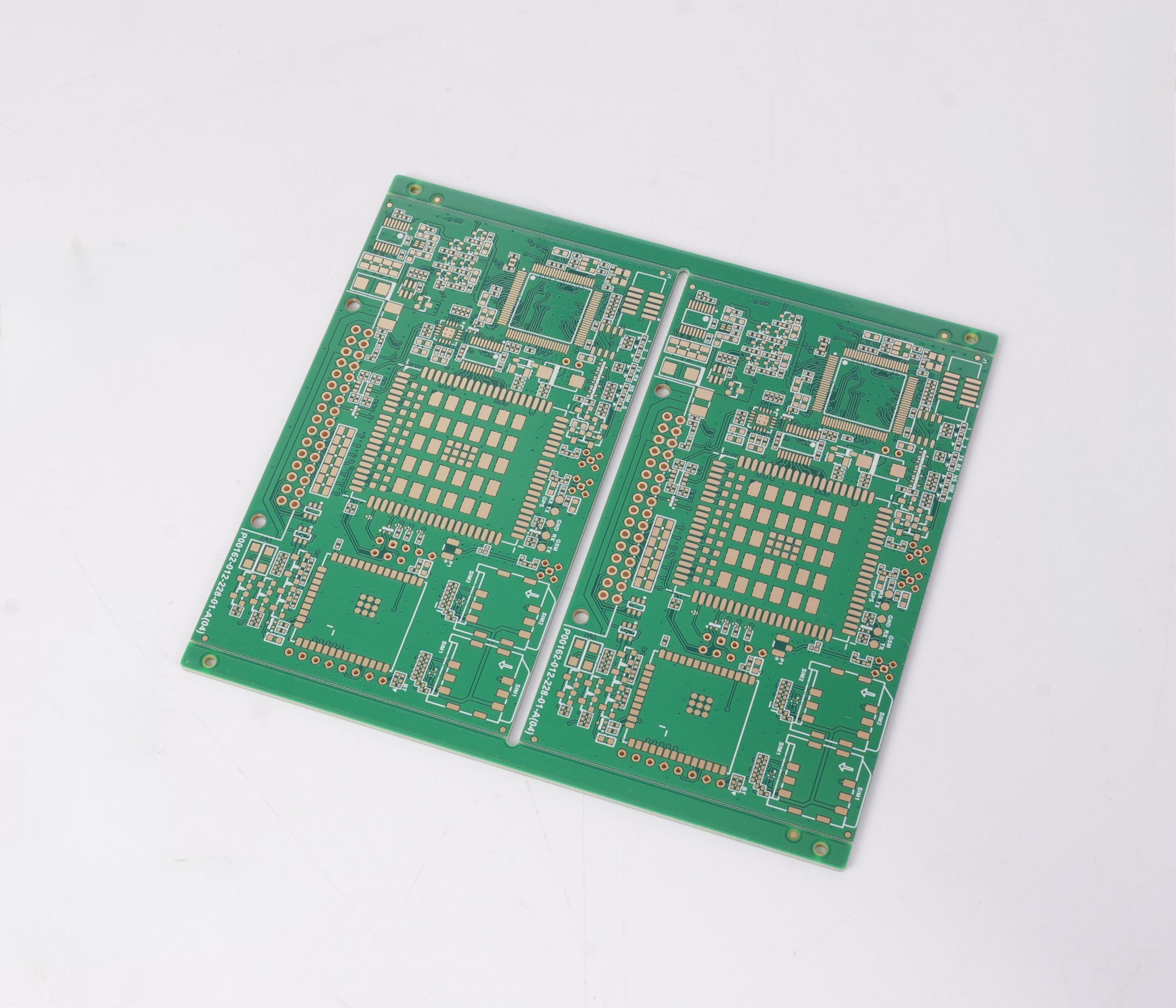
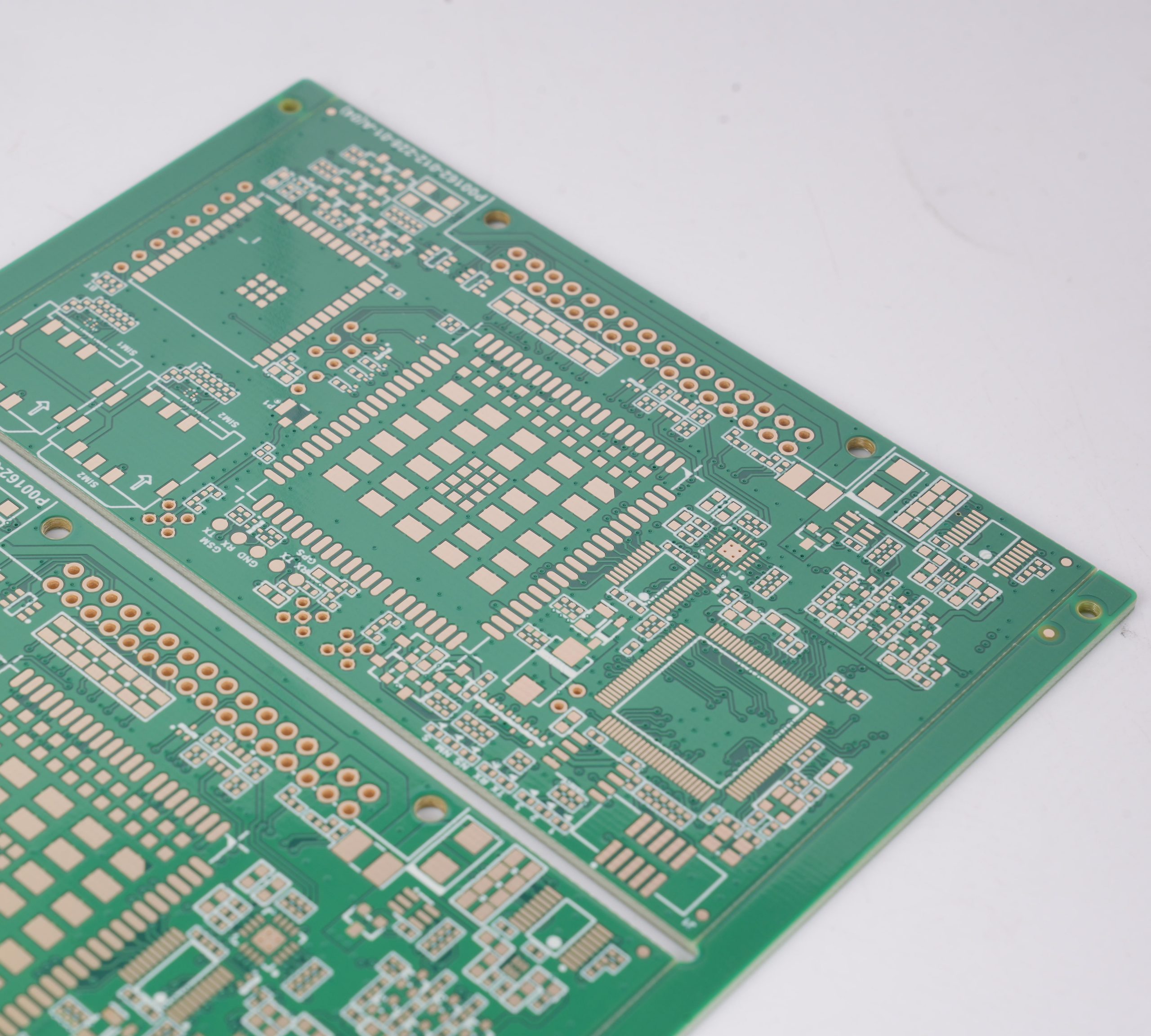
Standard double sided PCB is a printed circuit board with two layers of conductive circuits. Circuit layers are provided on both sides of the PCB and interlayer connections are achieved through conductive holes. It is suitable for a variety of electronic devices. Because of its relatively simple structure and low cost, it is a common basic circuit board type in electronic manufacturing.
What is a double-sided PCB?
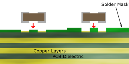
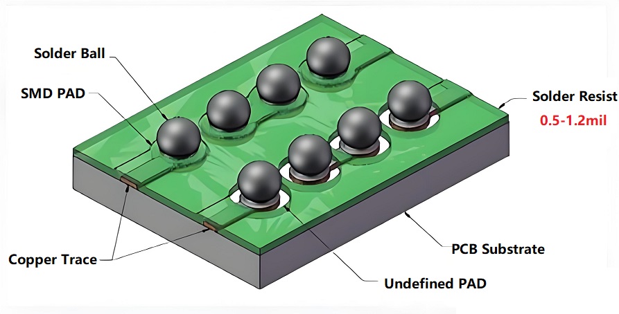
A double-sided PCB, also known as a two-layer PCB, features two layers of conductive material, typically copper, on both sides of an insulating substrate. These layers are interconnected using vias, which are small holes drilled into the PCB to allow electrical connections between the two sides.
Double-sided PCBs are used in applications where the complexity of the circuit requires components and connections to be placed on both sides of the board.
The primary advantage of a double-sided PCB is its ability to accommodate more components in a smaller footprint. This feature makes double-sided PCBs ideal for products where space is at a premium, such as smartphones, medical devices, and automotive electronics.
How many layers does a double-sided PCB have?
A standard double-sided PCB has two layers of conductive copper, one on each side of the substrate. These layers are electrically connected using vias, which create conductive paths between the two sides.
The number of layers in a PCB generally refers to the number of copper layers, which is why a double-sided PCB is made of two copper layers and an insulating substrate in between.

In contrast, multi-layer PCBs, which can have more than two layers of copper, are used for more complex circuits that require additional routing and signal pathways. A double-sided PCB is simpler in design and manufacturing compared to multi-layer PCBs but still offers significant flexibility for many applications.
What is the standard PCB layer?
In PCB manufacturing, a standard PCB layer refers to the number of copper layers used to create the circuit board. The standard PCB layer typically refers to the most common configuration in the industry, which is a single-layer PCB or double-sided PCB.
Single-layer PCBs consist of a single layer of copper, typically used for simpler, low-complexity circuits. These are ideal for products like basic household appliances, toys, and low-power applications.
Double-sided PCBs have copper layers on both sides, allowing for more complex circuits. These are used in products requiring more components, such as power supplies, automotive electronics, and communication devices.
While single-layer and double-sided PCBs are common, there are also multi-layer PCBs, which consist of three or more copper layers. These are used for even more intricate and densely packed electronic designs, such as those in high-frequency communication systems, medical equipment, and advanced computing devices.
What is the standard PCB format?
The standard PCB format typically refers to the physical dimensions and layout of the PCB, including the size, shape, and placement of components. In terms of manufacturing, standard PCB format can also refer to the specifications and designs that comply with industry standards for production.
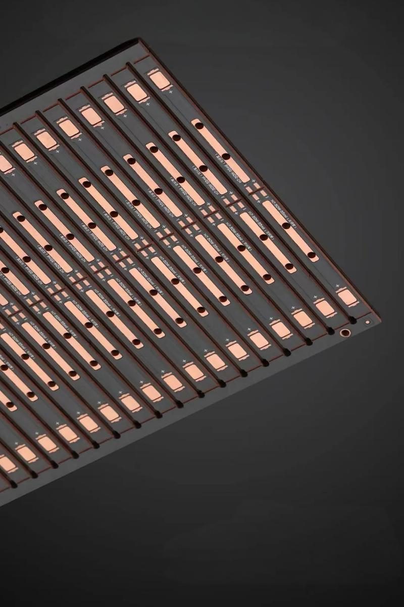
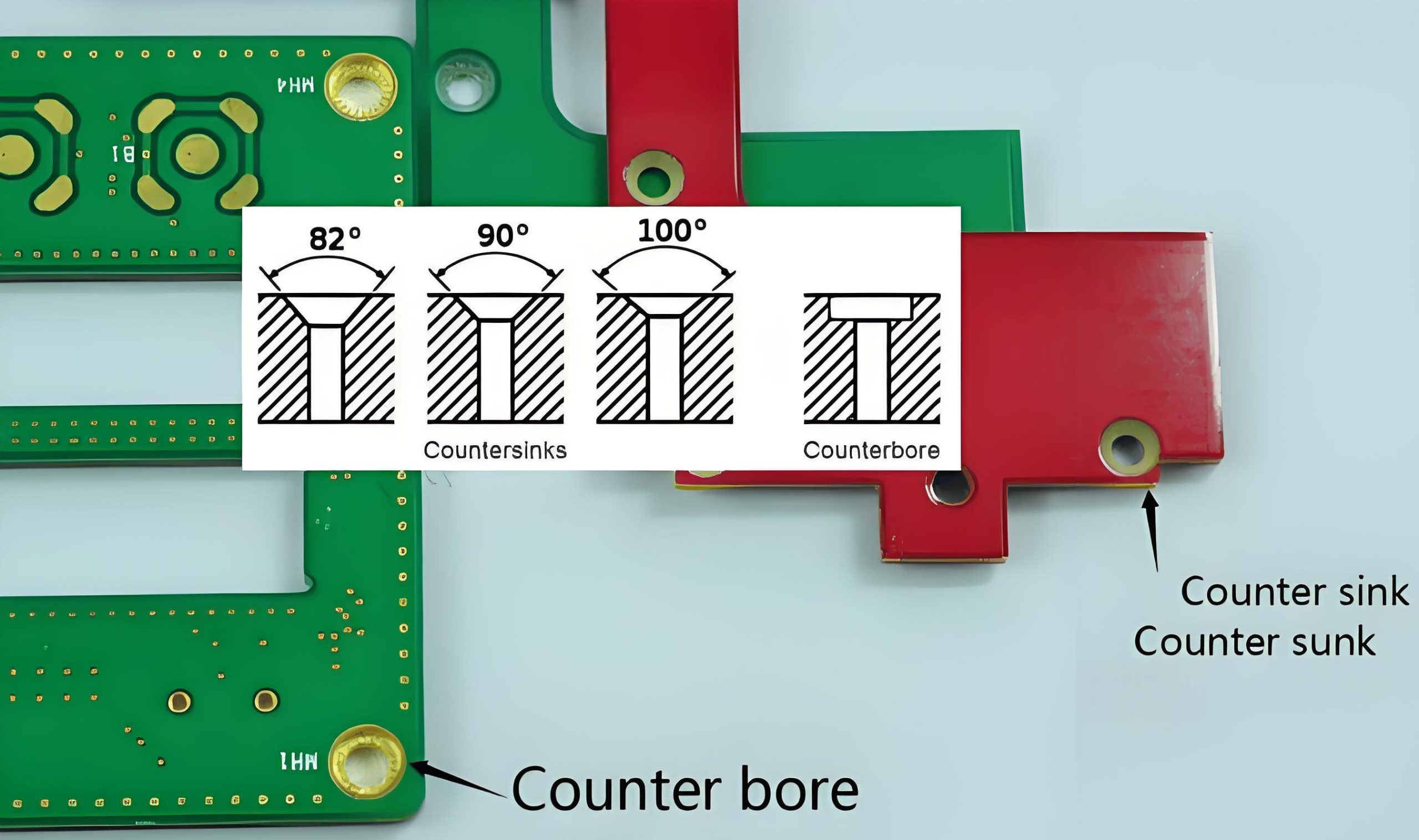
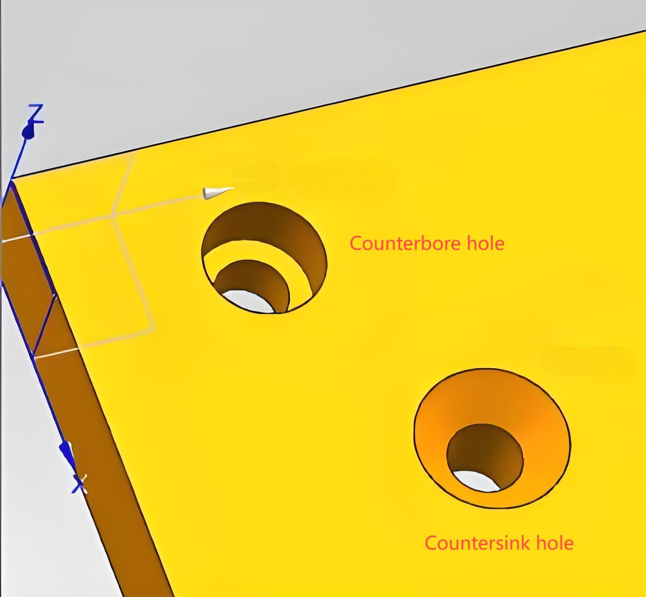
For double-sided PCBs, the layout should allow for efficient placement of components while maintaining electrical connectivity between both sides. The design also needs to ensure the copper traces are properly routed and connected through vias.
For boards that are mass-produced, standardization ensures consistency and compatibility with manufacturing processes, making it easier for designers to source components and for manufacturers to produce the boards at scale.
What is the standard FR-4 PCB?
FR-4 is a widely used material for PCB substrates, and standard FR-4 PCB refers to PCBs made from this material. FR-4 stands for Flame Retardant 4, which is a grade of fiberglass-reinforced epoxy resin. It is the most common material used for both single-layer and double-sided PCBs due to its excellent insulating properties, mechanical strength, and resistance to high temperatures.
The standard FR-4 PCB is durable, easy to fabricate, and provides good electrical insulation, making it suitable for a wide range of applications. It is also cost-effective, which is why it is used in everything from consumer electronics to industrial control systems.
While FR-4 is the most common material for standard PCBs, other materials, such as polyimide or ceramic, may be used in specialized applications that require specific thermal or electrical characteristics.
What are the requirements for a PCB board?
Designing a PCB board requires consideration of several key factors to ensure that the final product meets the desired performance, reliability, and cost-effectiveness.
Electrical Performance: The copper traces must be designed to handle the required voltage and current without overheating or causing signal degradation.
Thermal Management: Components that generate heat should be strategically placed to minimize temperature buildup.
Mechanical Strength: The material selected for the substrate (e.g., FR-4) plays a significant role in this aspect.
Size and Component Placement: A compact design is often required to save space, and the components must be placed optimally to reduce the overall size while maintaining proper functionality.
Meeting these requirements ensures that the final PCB product will be reliable and effective in its intended application.
What is the IPC standard for PCB?
The IPC standard refers to a set of guidelines and certifications established by the Institute of Printed Circuits (IPC), a global trade association for the electronics industry. The IPC standards are used by manufacturers to ensure that PCBs are fabricated to high quality and reliability standards.
For double-sided PCBs, the IPC-2221 standard outlines the design and manufacturing requirements for creating high-quality PCBs. This standard provides guidelines on design documentation, manufacturing processes, materials, and testing procedures to ensure that the PCBs meet the necessary performance, safety, and environmental requirements.
The IPC-610 standard, specifically, focuses on the acceptability of electronic assemblies, providing detailed requirements for the quality and performance of soldering, component placement, and overall PCB integrity.
What is the ISO standard for PCB manufacturing?
ISO standards are internationally recognized guidelines that help ensure consistency and quality in manufacturing. The ISO 9001 standard is the most widely adopted certification for quality management systems in PCB manufacturing. It ensures that manufacturers follow processes that consistently produce high-quality PCBs, including double-sided designs.
ISO certifications, such as ISO 14001 (environmental management) and ISO 13485 (medical devices), also apply to certain industries, ensuring that manufacturers comply with specific quality and safety standards relevant to their product’s end-use.
By adhering to these ISO and IPC standards, PCB manufacturers can ensure their products meet global expectations for quality, performance, and safety.
Conclusion:
Double-sided PCBs are a versatile and widely used type of printed circuit board. By offering components on both sides of the board, they allow for more complex circuits in a smaller, more compact design.
If you’re looking for standard double-sided PCB manufacturing or need assistance with your PCB design, EBest Circuit (Best Technology) can help. Reach out to us at sales@bestpcbs.com