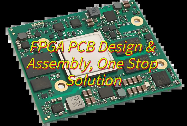
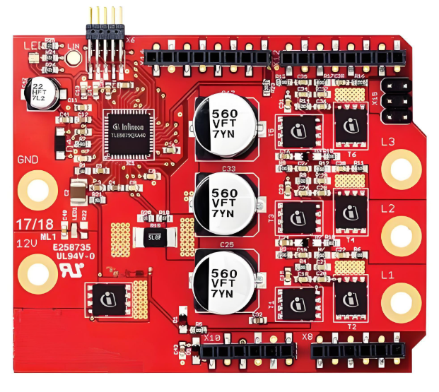
How to design A FPGA PCB? Discover its specification, benefits, application, and design guideline for FPGA PCB.
Can BGA welding withstand high temperature aging?
Why is my high-speed signal running slower and slower?
Will multiple power supplies fight with each other?
EBest Circuit (Best Technology) Can Provide You:
Welding perspective: Each board is X-rayed, and solder joint defects are nowhere to be hidden.
Signal highway: From drawing board to assembly, the signal is fully escorted.
Power traffic light: Intelligently adjust the power-on timing to prevent power supply chaos.
Welcome to contact us if you have any request for FPGA PCBA service: sales@bestpcbs.com.
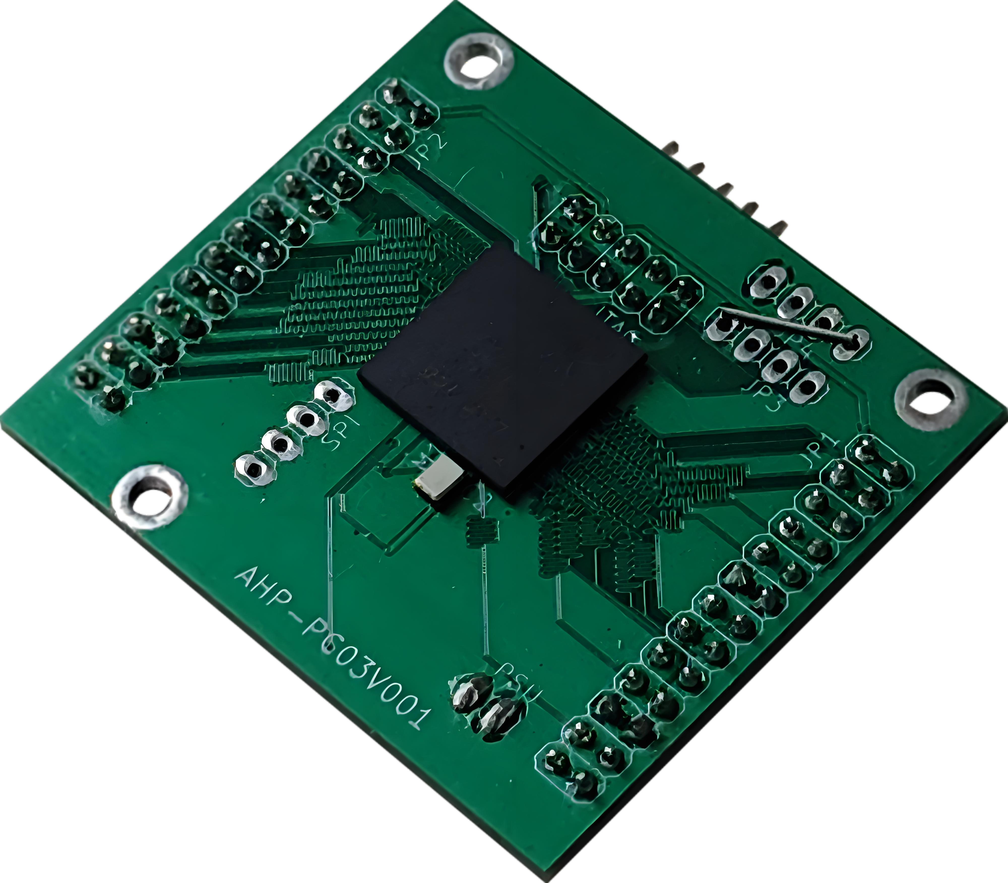
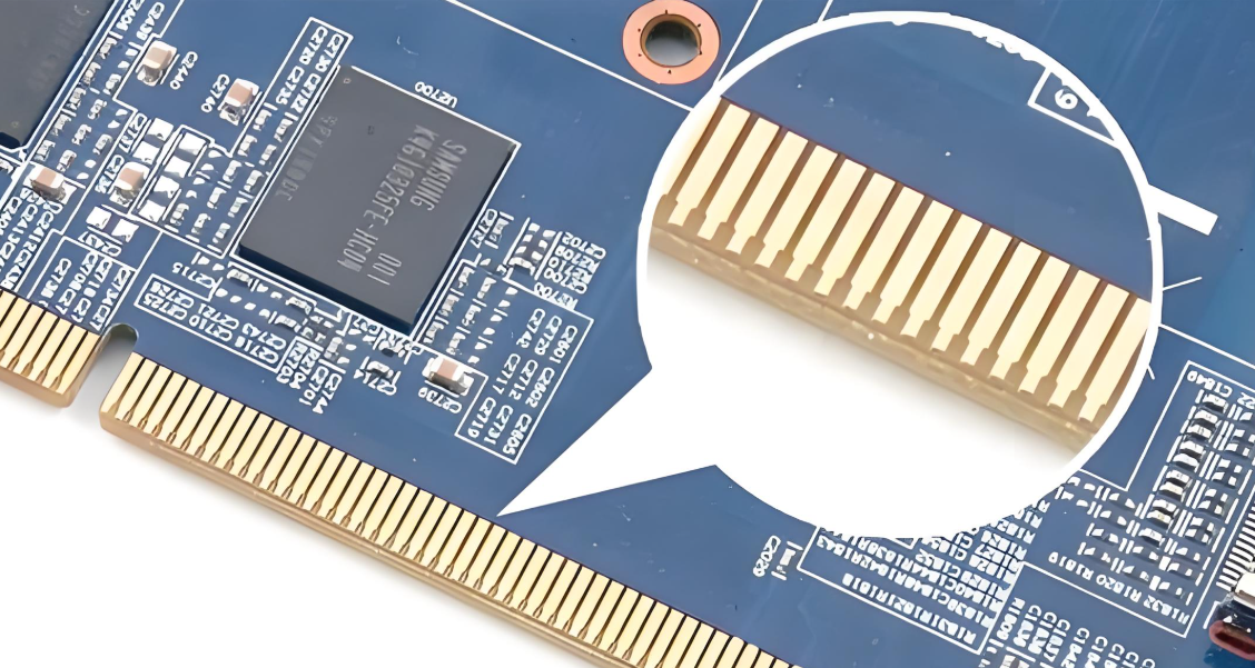
What Is FPGA PCB?
A FPGA PCBis a specially engineered printed circuit board that physically mounts and electrically integrates a field-programmable gate array semiconductor device with supporting hardware components, such as power regulators, memory units, clock sources, and input/output connectors.
This substrate features precisely routed copper traces to establish reliable electrical pathways, incorporating design elements for signal integrity in high-speed interfaces, stable multi-voltage power delivery, and efficient thermal dissipation to manage operational heat.
Once assembled, the board serves as a reconfigurable platform capable of implementing custom digital logic functions through post-manufacturing programming of the FPGA, enabling versatile applications like real-time data processing or communication bridging.
DFM Optimization – Early design feedback to minimize re-spins.
Flexible Packaging – Support for advanced ICs (BGA, QFN, 01005).
Free DFM (Design for Manufacturability) Analysis: Optimizes PCB layouts to reduce material waste, lower production costs, and avoid late-stage design revisions.
Turnkey Solutions – Full-service PCB manufacturing from design to delivery, accelerating your product’s time-to-market.
Superior Quality – 100% inspection on bulk orders, ensuring reliability and consistency.
Fast Turnaround – 24-hour rapid prototyping and industry-leading production lead times.
Stable Supply Chain – Guaranteed material availability with minimal risk of delays.
Competitive & Transparent Pricing – No hidden costs, offering the best value without compromising quality.
Our PCBA Capabilities
Item
Capabilities
Placer Speed
13,200,000 chips/day
Bare Board Size
0.2 x 0.2 inches – 20 x 20 inches/ 22*47.5 inches
Minimum SMD Component
01005
Minimum BGA Pitch
0.25mm
Maximum Components
50*150mm
Assembly Type
SMT, THT, Mixed assembly
Component Package
Reels, Cut Tape, Tube, Tray, Loose Parts
Lead Time
1 – 5 days
FAQs
Q1: Why does my FPGA PCB fail to boot consistently after assembly? A1: Check solder joint integrity – BGA voids exceeding 25% cause intermittent connections. Use X-ray inspection to verify void percentage. Ensure power sequencing matches FPGA datasheet requirements (typically core voltage before I/O banks).
Q2: How to resolve signal integrity issues in 10Gbps+ transceiver channels? A2: Route differential pairs with <5mil length mismatch and insert ground-stitching vias every 150mil near SerDes lanes. Simulate with IBIS-AMI models to validate eye diagram margins pre-production.
Q3: Why do we encounter timing closure failures despite meeting constraints? A3: Clock skew often originates from unequal via counts in global clock trees. Balance H-tree routing with matched via transitions (typically 8 vias per branch). Add programmable delay buffers for ±50ps fine-tuning.
Q4: What causes thermal runaway in high-density FPGA designs? A4: Inadequate copper thickness in power planes (recommend 2oz for >15A currents). Implement thermal relief patterns under BGA with 0.3mm diameter voids. Monitor junction temperature using on-die sensors via I2C.
Q5: How to mitigate EMI from high-speed memory interfaces? A5: Apply π-type EMI filters to DDR4 DQ lines (22Ω resistors + 100pF caps). Stagger memory chip placement to break resonant cavity effects. Use shielded flex cables for off-board connections exceeding 3Gbps.
If you’ve ever wondered how your LED lights work or thought about building your own lighting system, understanding LED light circuit board design is the perfect place to start. From simple desk lamps to advanced automotive lights, LED circuit boards power nearly every type of modern lighting. These boards are more than just a place to hold LEDs—they help control current, manage heat, and ensure your lights stay bright and stable.
What Is an LED Light Circuit Board?
An LED light circuit board is a printed circuit board (PCB) specially designed to support and power light-emitting diodes (LEDs). It provides a stable platform where LEDs are mounted and connected through copper traces that guide the current flow.
These boards are used everywhere—home lights, office lighting, headlights, signs, and electronic displays. What makes LED PCBs stand out is their ability to manage heat. Since LEDs generate heat while working, especially high-brightness ones, the PCB helps transfer that heat away. Many of these boards are made of aluminum or use metal-core designs to improve thermal performance.
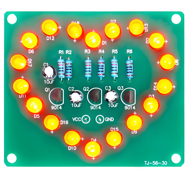
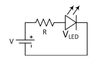
LED Circuit Board Diagram
A circuit diagram is like a map of your LED board. It shows how the parts connect to each other and how electricity flows. This is where you plan your setup before building the actual board.
In this example:
VCC is the power supply (like a 12V battery or adapter)
The resistor limits the current
The LED lights up as current flows from positive to ground
In real boards, especially SMD LED PCB boards, this wiring is replaced with copper tracks. The LEDs are surface-mounted, meaning they’re soldered directly on the board. Multiple LEDs can be placed in series, parallel, or a combination, depending on your application.
You’ll also see labels for input voltage, ground, and other components like capacitors, diodes, or voltage regulators if your board is more advanced.
LED Light Circuit Board Design Guide
If you want to design an LED light circuit board for commercial or long-term use, there are a few more things to consider beyond a simple circuit.
1. Choose the LED Type Wisely
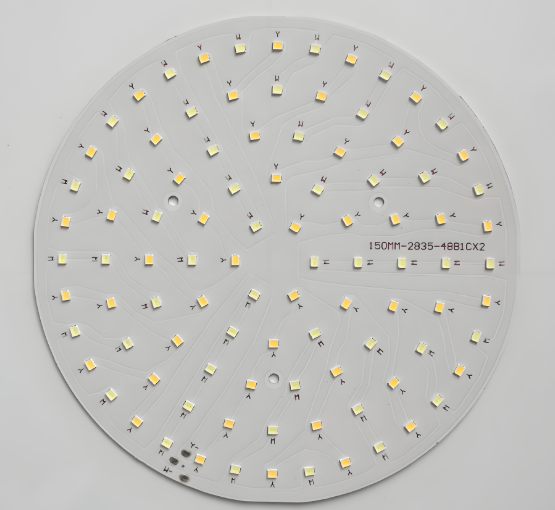
Your LED type affects layout, current, and heat. For general lighting, SMD LEDs (such as 2835 or 5050 types) are common. For signage or high-power use, COB LEDs may be better.
2. Decide on Board Material
If your LEDs run hot, like in street lights or industrial lights, go for aluminum or metal-core PCBs. These manage heat much better than traditional FR4 boards. Below is a LED pcb board used aluminum base.
3. Include Heat Management
Use thermal vias, heat sinks, or thicker copper layers if the board carries high currents. Heat buildup can shorten LED life or reduce brightness.
4. Control Current
Never rely on direct voltage for LEDs. Use resistors or constant current drivers. LEDs create heat, especially if many are packed closely. Too much heat lowers their lifespan. Good thermal design includes:
Thick copper layers (≥1oz)
Thermal vias under LED pads
Aluminum base to move heat away
Heat sinks or thermal pads if needed
5. Pay Attention to Trace Width
High currents need wider traces. Use trace calculators to ensure your copper width is suitable. Also, avoid sharp 90° turns—these can stress the signal and cause EMI problems. Use 45° angles to keep signals smooth and reduce heat buildup.
6. Place Components Smartly
Keep resistors close to the LEDs. Separate power and signal lines. Leave space for heat dissipation or mounting. Some other tips including:
Place resistors near the LED they control
Keep power and ground lines wide and short
Group similar LEDs in rows or grids
Leave space for mounting holes or connectors
Keep heat-generating parts away from sensitive ones
7. Test Points and Labels
Add test pads for checking voltage and current during production or troubleshooting. Label input/output pads clearly to help during assembly. Here is a guide of how to make LED circuit board.
How Many LED Light Fixtures Can Be on One Circuit?
This question comes up a lot in home lighting and commercial installations. The answer depends on how much power each fixture uses and what the circuit breaker rating is.
Let’s break it down:
A standard 15A breaker on 120V power provides 1800 watts.
A 20A breaker gives you 2400 watts.
Suppose each LED fixture consumes 10 watts. Then on a 15A circuit:
1800W / 10W = 180 fixtures
But you should never use 100% of the circuit’s capacity. A safe rule is to use up to 80%.
So, the real number is:
1800W × 0.8 = 1440W → 144 LED fixtures (10W each)
What Happens If You Wire an LED the Wrong Way?
LEDs are diodes, which means they conduct electricity in one direction only. If you connect them backward:
They won’t light up because current can’t flow
In some cases, if voltage is too high, the LED might get damaged
This is why LED symbols in diagrams have a direction (anode to cathode). Many modern circuits include a protection diode or a reverse-polarity safeguard to prevent damage.
Always double-check before soldering or applying power. Getting the polarity right is crucial for the LED to work.
Should I Put a Resistor Before an LED?
Yes. A resistor is essential unless you’re using a regulated current driver.
LEDs don’t limit their own current. If you connect them directly to a power supply, even at a “safe” voltage, they can draw too much current, overheat, and burn out.
The resistor acts like a gate. It lets the right amount of current pass through and drops the extra voltage. Even LED strips usually have built-in resistors. For DIY boards, always calculate and add the correct resistor for every LED or LED group.
LED Board Design Price
The LED board design price depends on several factors:
Factor
Cost Impact
Board Size
Larger boards cost more
LED Type (SMD vs. COB)
COB boards may be pricier
PCB Material (FR4 vs. Aluminum)
Aluminum is more expensive
Quantity
Larger batches lower per-board cost
Layers
Multilayer boards cost more
Assembly Required
Soldered boards cost extra
Typical costs for LED circuit boards:
Basic LED board (single-layer FR4): $0.50 – $2 per piece
Aluminum SMD LED board: $1 – $4 per piece
Custom-designed and assembled board: $5 – $20 depending on design complexity
For mass production, you can get volume discounts and better pricing through professional LED PCB manufacturers like EBest Circuit (Best Technology). We provide free DFM checks, fast quotes, and one-stop services including prototype to volume production.
FAQs
1. What is a SMD LED PCB board?
It’s a printed circuit board designed to mount Surface-Mounted Device (SMD) LEDs directly onto the board, used in lighting panels, strips, and signs.
2. How long does an LED circuit board last?
With good design and cooling, LED boards can last 30,000 to 50,000 hours or more.
3. Can I connect LEDs in series or parallel?
Yes. Series connections share the same current; parallel connections share the same voltage. Choose based on your power source.
4. What software should I use to design LED boards?
KiCAD, Altium Designer, EasyEDA, and Eagle are commonly used tools for creating LED PCB layouts.
5. What happens if you put too many lights on a circuit?
If you connect too many LED lights to one circuit, the total power draw may exceed the circuit’s capacity. This can lead to overloaded breakers, flickering lights, or even tripped fuses. In worst cases, wires may overheat, posing a fire risk.
If you’re planning to build or order custom LED light circuit boards, EBest Circuit (Best Technology) is ready to help. We support everything from LED PCB board quick-turn prototypes to mass production, all with professional engineering support and strict quality checks.
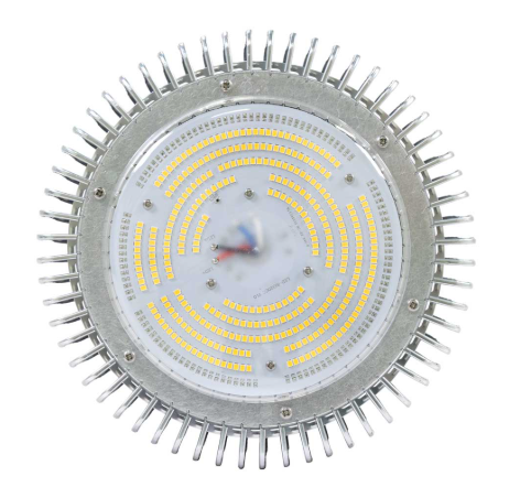
A round high bay LED light is a type of industrial lighting fixture used in buildings with high ceilings—usually more than 20 feet. These lights are designed in a circular or UFO-style shape to evenly distribute light over large areas. You’ll often find them in warehouses, gymnasiums, factories, airports, and retail stores. Compared to older metal halide or fluorescent systems, round high bay LED lights are more energy-efficient, last longer, and require less maintenance.
Each fixture typically contains multiple high-power LEDs mounted on a metal-core PCB, surrounded by a reflector and protected by a lens. These components are arranged to direct intense, bright light downward to cover a wide area. The circular layout is easy to install, especially for ceilings where centralized lighting is needed.
Do High Bay LED Lights Get Hot?
Yes, high bay LED lights can get hot—especially after extended use. Although LEDs are more efficient than traditional lighting sources, they still generate heat during operation. The more powerful the light (for example, 100W, 150W, or 200W round high bay fixtures), the more heat it produces.
Unlike incandescent or halogen lights, LEDs don’t emit heat through infrared radiation. Instead, their heat builds up internally around the chip and must be conducted away through the PCB and heat sink. If the heat isn’t managed properly, it can reduce the light’s efficiency, shorten the LED’s lifespan, and even cause failure. That’s why thermal management is crucial for high bay LED lights—and why aluminum PCBs are widely used in their construction.
Why Use Aluminum PCB for High Bay LED Lights?
Aluminum PCBs are preferred in round high bay LED lights because they offer excellent thermal conductivity. In high bay environments, LED chips are packed closely together on a board, creating a concentrated source of heat. Aluminum PCBs help move this heat away from the chip quickly, reducing the risk of overheating.
Traditional fiberglass PCBs (like FR4) are not good at handling thermal loads. They trap heat near the components, which can lead to LED failure. In contrast, aluminum PCBs consist of a metal base layer, a dielectric insulation layer, and a copper circuit layer.
Using aluminum PCBs in high bay LED lights also helps to maintain consistent brightness, reduce light degradation over time, and support longer operating lifespans—often 50,000 hours or more.
Advantages of Using Aluminum PCB
1. Aluminum PCBs rapidly transfer heat away from LED chips, so that they can reduce the temperature at the LED junction and maintains stable light output over time.
2. High bay lights are often used in demanding environments like factories and warehouses. The base material of aluminum PCB is metal, so they can provide better structural stability and resistance to vibration and moisture.
3. When LEDs operate at lower temperatures, their lumen output remains consistent for years with minimal degradation.
4. Despite their strength, aluminum PCBs are relatively lightweight compared with copper core PCB. This can reduce the overall weight of the high bay fixture, make it easier to install and handle.
5. Though aluminum PCBs cost more than standard FR4 boards, their durability, reliability, and low maintenance result in long-term savings—especially in industrial settings where lighting failures can be costly.
1W vs 2W vs 3W Aluminum PCB: Which One Is Best?
In aluminum PCBs used for round high bay LED lights, the terms 1W, 2W, and 3W refer to the thermal conductivity of the dielectric layer between the copper circuit and the aluminum base, not the power of the LEDs themselves.
It’s measured in watts per meter-kelvin (W/m·K) and indicates how efficiently heat is transferred from the copper to the aluminum core. The main job of dielectric layer is to insulate electrically while conducting heat away from the LED components. Here’s how they compare:
1W Aluminum PCB
1W PCBs are used for low-power applications where heat is minimal. They’re suitable for small or decorative lights but not recommended for industrial high bay systems. The heat dissipation capacity is limited, and using them in high-power lights may cause overheating.
2W Aluminum PCB
2W PCBs offer better heat conductivity than 1W versions and are often used in mid-power LED lights, such as 50W to 100W systems. They provide a balance between performance and cost, and they work well in moderately demanding environments.
3W Aluminum PCB
3W PCBs are designed for high-performance LED lighting. They are ideal for 150W to 200W round high bay fixtures, where multiple high-output LEDs are densely packed. These boards handle more heat and offer higher durability under continuous operation.
So, which one is best? For round high bay LED lights used in industrial or commercial buildings, 3W aluminum PCBs are usually the best option. They support powerful LEDs, provide excellent thermal control, and reduce the risk of system failure.
Round High Bay LED Lights PCB Design Guide
Designing a printed circuit board (PCB) for round high bay LED lights requires special attention to thermal management, electrical performance, mechanical stability, and spatial efficiency. These lights operate in high-ceiling environments and typically involve high power, which means the PCB must handle significant heat while maintaining long-term reliability.
1. Shape and Form Factor
Since the fixture is round, the PCB is typically designed in a circular shape to match the housing and ensure symmetrical light distribution. This helps maintain uniform brightness across the target area and improves heat spreading across the surface.
To design the board:
Use radial symmetry when placing LED chips to maintain uniform light output.
Create concentric LED rings to balance thermal and optical performance.
Align mounting holes and cutouts with the housing’s mechanical features for secure fitting.
2. Material Selection: Aluminum Core
The aluminum substrate is the foundation of thermal performance. Choose high-quality aluminum cores with good thermal conductivity—typically in the range of 1.0 W/m·K to 3.0 W/m·K.
Common material stack-up:
Top layer: Copper circuit (usually 1oz or 2oz)
Middle layer: Dielectric insulating layer (optimized for thermal transfer, usually 75–150μm thick)
Bottom layer: Aluminum base (typically 1.0–1.6mm thick)
Noted: The thicker the base, the higher the dielectric layer value, the better the heat transfer, but also the heavier and costlier the board becomes.
3. Copper Thickness and Trace Width
For high-power LEDs, the copper thickness should be:
1oz (35μm) minimum for moderate power (≤100W)
2oz (70μm) or 3oz (105μm) for high-power designs (≥150W)
Use wide copper traces to reduce resistive losses and avoid overheating. Calculate trace width based on expected current using IPC-2221 standards.
4. Thermal Management Techniques
Heat dissipation is critical in high bay LED lights. Key design methods include:
Use direct thermal path: Use thermally conductive vias or metal-core structures to transfer heat from LEDs to the aluminum base.
Thermal vias: For multilayer aluminum PCBs (if needed), add thermal vias below heat-generating components to improve vertical heat flow.
5. LED and Component Placement
Carefully plan the placement of LEDs, drivers, resistors, and protection components:
LEDs: Distribute evenly in radial or concentric patterns to ensure uniform illumination.
Driver ICs and capacitors: Place these in cooler areas away from dense LED zones to reduce thermal interaction.
Thermistors or temperature sensors: Add for real-time temperature monitoring and safety.
Since aluminum is conductive, electrical insulation is critical. The dielectric layer between the copper circuit and aluminum base must withstand at least 2–3kV isolation voltage. It is better to consult your PCB manufacturer to get a best solution.
Our Aluminum PCB Manufacturing Capability
Item
Capabilities
Layer Count
1 – 10 Layers
Max Board Dimension
24” × 64” (610mm × 1625mm)
Min Board Thickness
0.6mm
Max Board Thickness
4.0mm
Conductor Thickness
0.5oz – 10oz
Min Line Width/Line Space
4/4mil (0.10/0.10mm)
Min Hole Diameter
10mil (0.25mm)
Min Punch Hole Diameter
0.12” (3.0mm)
Min Hole Spacing
16mil (0.4mm)
Min PAD Ring (Single)
3mil (0.075mm)
PTH Wall Thickness
Normal: 0.59mil (15μm); HDI: 0.48mil (12μm)
Min Solder PAD Diameter
14mil (0.35mm)
Min Soldermask Bridge
8mil (0.20mm)
Min BAG PAD Margin
5mil (0.125mm)
PTH/NPTH Dia Tolerance
PTH: ±3mil (0.075mm); NPTH: ±2mil (0.05mm)
Where Can I Get an Aluminum PCB Quote?
If you’re sourcing aluminum PCBs for round high bay LED lights, it’s important to choose a supplier with experience in LED lighting applications. Getting the right material, thickness, and thermal configuration can make a big difference in your product’s performance.
EBest Circuit (Best Technology) is a professional PCB manufacturer offering customized aluminum PCBs for LED lighting. We support a wide range of applications, from low-power LED modules to high-power round high bay LED lights. Our services include:
Custom shapes PCB designs, like round, rectangle, irregular…
Various materials available, aluminum, copper, FR4, ceramic and so on
3W aluminum PCB production
Fast prototyping and mass production
Strict quality control ISO quality control system
Competitive pricing and fast delivery
No MOQ & fully flexible
Turnkey services from PCB design, components sourcing to PCB assembly
SMT factory both in China & Vietnam
To get a free aluminum PCB quote, simply send us your design files or requirements. Our engineering team will review your project and offer the best solution based on your needs and budget.
If you’re ready to start a new LED lighting project or improve your current product line, partnering with EBest Circuit (Best Technology) can help to save time, reduce costs, and deliver reliable lighting solutions to you.
FAQs
1. What material is used in aluminum PCBs for high bay lights?
Aluminum PCBs use a base of aluminum metal, a dielectric layer for insulation, and a copper layer for circuit routing. This stack helps transfer heat from the LEDs to the fixture housing efficiently.
2. Can I use FR4 PCB in round high bay LED lights?
FR4 can be used for very low-power LEDs, but it’s not suitable for high bay lights due to poor heat dissipation. Aluminum PCBs are much more reliable in these applications.
3. Can aluminum PCBs be multilayered?
Yes, but multilayer aluminum PCBs are complex and more expensive. Most LED lights use single or double-layer aluminum boards.
4. What’s the standard thickness for aluminum PCBs?
The base thickness usually ranges from 1.0mm to 1.6mm. Copper thickness varies from 1oz to 3oz, depending on current load requirements.
5. How can I get a quote for custom aluminum PCBs?
You can contact EBest Circuit (Best Technology) with your design files or specifications. We offer fast quoting, engineering support, and manufacturing tailored to your LED lighting project.
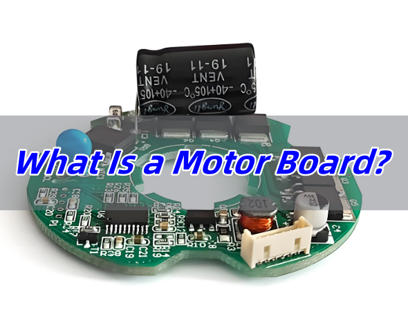
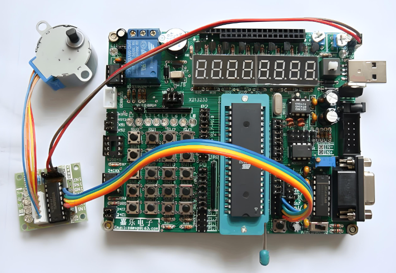
A motor board is a key part of any system that controls electric motors. Whether you’re building a small robot, a smart curtain, or a DIY RC car, the motor board is the part that connects your brain (the microcontroller) to your muscle (the motor).
You cannot connect a motor directly to an Arduino, Raspberry Pi, or other microcontroller because motors need more power than these boards can handle. That’s where a motor driver board comes in. It supplies power and manages direction, speed, and safety.
In this guide, we’ll explore what a motor board is, the types available, how it works, and why it’s so important for any project with moving parts.
What Is a Motor Board?
A motor board is a small printed circuit board (PCB) designed to control electric motors. It acts like a translator between your low-power controller and your high-power motor. You send simple signals to the board, and the board powers and controls the motor for you.
Motor boards are often used in robotics, automation systems, and electric vehicles. They are essential when you want to move wheels, turn gears, lift arms, or rotate anything using a motor.
They can work with different types of motors, such as:
DC motors
Stepper motors
Servo motors
Brushless DC motors (BLDC)
Each motor type may require a different kind of motor board.
What Does Motor Board Mean?
The term motor board means a circuit board made specifically for motor control. It includes components like driver chips, power inputs, connectors, and sometimes sensors.
In simple terms, it’s a smart power switch. You tell it what to do (via signals from a microcontroller), and it supplies the right amount of power to the motor.
For example, when building a robot, the main board might handle logic, sensors, and communication. The motor board only deals with moving the wheels. That separation makes the system more reliable and easier to design.
Types of Motor Board
There are many types of motor boards, and each one is built to handle specific motors or motion requirements. Here are the most common:
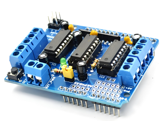
1. DC Motor Driver Boards
These are used for basic motors that rotate in one direction or both. You can control speed and direction using PWM (pulse width modulation) and digital pins. A popular example is the L298N motor driver board, which can run two DC motors at once.
2. Stepper Motor Boards
Stepper motors move in fixed steps, not continuous rotation. These are great for projects that need precise movements, like 3D printers or CNC machines. Boards like the A4988 or DRV8825 are common choices. They control the step rate and direction.
3. Servo Motor Boards
Servos move to specific angles. They are used in robotic arms, RC cars, and camera gimbals. Servo boards control the angle through a PWM signal. Some boards allow you to connect many servos at once for large projects.
4. Dual H-Bridge Motor Boards
An H-Bridge lets current flow in both directions through a motor. This means your motor can spin forward or backward. A dual H-bridge board like the L298N or L293D can control two DC motors independently.
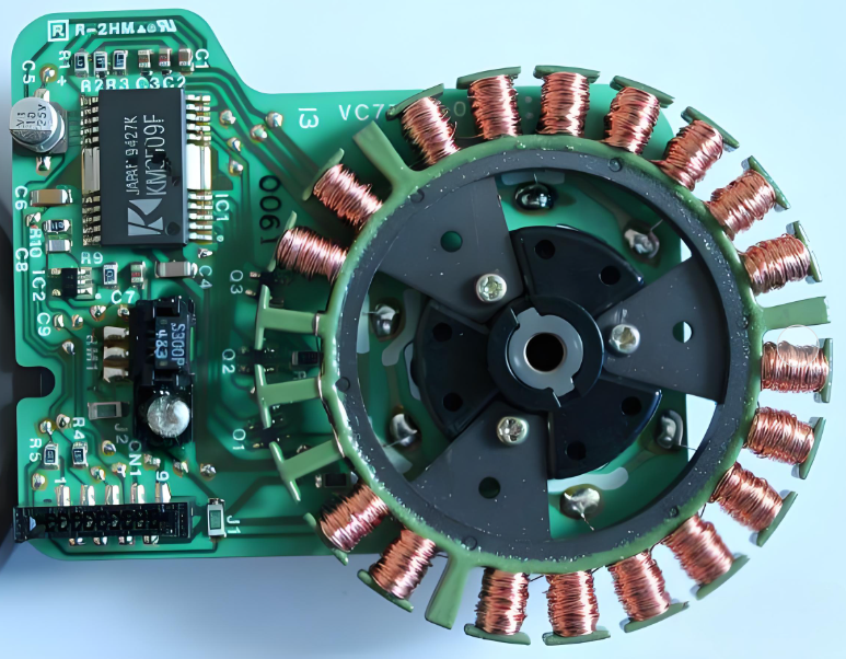
5. Brushless DC Motor (BLDC) Boards
BLDC motors are used in drones, electric skateboards, and industrial tools. They need more complex driver boards that handle three-phase power and feedback from position sensors. These boards often include FETs, controllers, and overcurrent protection.
6. Electric Motor Boards for Vehicles
These high-power boards control large motors in e-bikes or scooters. They usually feature thermal sensors, regenerative braking, current limiters, and fault indicators. They are more robust than typical hobby motor boards.
What Does a Motor Driver Board Do?
A motor driver board takes control signals from a microcontroller and uses them to control the motor’s power. It does several important jobs:
Amplifies signals: Microcontrollers output low voltage. Motor driver boards boost these to match motor power requirements.
Controls direction: By switching current direction, the motor can spin forward or backward.
Adjusts speed: PWM signals let you change motor speed smoothly.
Protects components: Built-in diodes or protection chips guard against backflow current (back EMF), which can harm your controller.
Manages current: Some drivers limit current to prevent motor or circuit damage.
So, the motor driver board is the part that makes motors usable with small electronics.
What Color Is a Motor Board Usually?
Most motor boards are green, the standard color for PCBs. This green color comes from the solder mask, which protects the copper traces underneath.
However, boards also come in:
Red – used by SparkFun and many other hobby suppliers
Blue – seen in some open-source projects
Black – popular for higher-end or custom boards
Yellow or White – rarely used but available
The color doesn’t affect performance. It’s just for looks and branding. Pick based on function, not color.
How to Make a Motor Board?
If you want to build your own motor board, here are the basic steps:
1. Choose Your Motor
Decide if you’re using a DC, stepper, or servo motor. Each needs a different driver.
2. Pick a Driver Chip
Choose a suitable IC:
L298N for two DC motors
A4988 for stepper motors
TB6612FNG for better efficiency
3. Design the Circuit
Use PCB design software like: KiCad, EasyEDA, Eagle. Include connectors, capacitors, and resistors as needed. Add power input terminals and logic pin headers.
4. Create the PCB
You can:
Order from a PCB maker online like PCBway (lowest price but poor quality) or EBest Circuit (Best Technology) (competitive price with higher quality and 5 years quality guarantee).
Etch it manually at home (not recommended for beginners)
5. Assemble the Board
Solder all components. Double-check the orientation of ICs, diodes, and power connections.
6. Test It Safely
Start with a small motor. Use a current-limited power supply. Test using an Arduino with simple code.
Building your own board is a great learning project, but for complex systems, buying a tested module is safer and faster.
Why Do You Need a Motor Driver?
Microcontrollers are smart, but they’re weak when it comes to power. Motors often need 6V–24V and 1A or more. An Arduino pin provides only 5V and about 20–40mA.
If you connect a motor directly to the microcontroller, two things might happen:
1. The microcontroller resets or freezes
2. The motor doesn’t spin—or worse, the controller burns out
A motor driver board solves this. It protects your control board while giving the motor what it needs.
It also adds:
Precise control (change speed or reverse easily)
Electrical isolation in some cases
Protection features like thermal shutoff or current limiting
So, every project with motors—big or small—should include a driver.
What Is the Use of a Motor Driver Board?
A motor driver board is used in any system that requires motion. Here are some common uses:
1. Robotics
From mobile robots to robotic arms, motor drivers control wheels, joints, and actuators. You can run multiple motors and coordinate movement smoothly.
2. Automation
In smart homes and factories, motors open doors, close blinds, or move conveyor belts. Motor boards provide the control logic behind these actions.
3. Drones and RC Vehicles
Brushless motor driver boards keep drones stable and responsive. In RC cars, motor boards drive wheels, steering, or servo-based suspension.
4. 3D Printers and CNC Machines
These use stepper motor drivers to move the nozzle or cutter precisely. Each axis has its own board.
5. Electric Bikes and Scooters
High-current boards manage wheel motors, brakes, and regenerative systems.
A motor board is more than just a piece of hardware—it’s the control center that makes electric motors useful in real projects. Without one, your motor can’t respond to speed or direction commands, and your controller may get damaged trying to power it directly.
There are many types of motor boards, from basic DC motor drivers to advanced BLDC boards used in EVs. You can buy them off the shelf or design your own if you’re building a custom system. Whether you’re working on a robot, a drone, or a smart appliance, the motor driver board is a must-have. It turns signals into motion, safely and efficiently.
FAQs
1. Can I run a DC motor without a motor board?
You can, but it’s risky. Motors draw more current than microcontrollers can handle. You could damage your board.
2. What is the best motor driver board for beginners?
The L298N is affordable, easy to use, and works with most Arduino projects.
3. Can a motor board control more than one motor?
Yes. Dual motor boards control two motors. Some advanced boards can control four or more.
4. Are all motor boards compatible with all microcontrollers?
Not always. Check the logic level (3.3V vs. 5V) and connection type. Most hobby boards are designed for Arduino compatibility.
5. Is it safe to build your own motor board?
Yes, with proper design and low-voltage testing. Always double-check your connections and power ratings.
What is a VFD control panel? This guide comprehensively covers its components, functions, installation, wiring, design, manufacturer selection, and cost analysis.
Does your VFD control panel have poor heat dissipation and short life due to poor PCB design?
Is the delivery delayed due to unstable supply chain, affecting the project progress?
Traditional solutions are costly and slow to iterate. How to balance performance and cost performance?
EBest Circuit (Best Technology) Can Provide Service:
One-stop PCBA service – control the entire process from design to mass production, optimize the heat dissipation layout, and improve the durability of the panel by 30%+.
Agile supply chain – own PCB factory + strategic cooperation component supplier, ensure fast delivery within 15 days, error rate <0.5%.
Cost optimization solution – provide high compatibility circuit design, support flexible iteration, and reduce batch cost by 20%.
What Is VFD Control Panel?
AVFD control panel is the dedicated operator interface unit for managing variable frequency drives (VFDs), providing direct controls to start, stop, and adjust motor speed or torque through tactile buttons, digital displays, and parameter-setting menus. It enables real-time monitoring of operational status including frequency output, current levels, and fault diagnostics while supporting both manual inputs and automated external signal integration via communication terminals. The panel features protective enclosures for industrial environments, application-specific configuration options, and energy optimization capabilities through precise motor speed regulation based on load requirements.
VFD Control Panel Components & Specification
Component
Specification
Power Conversion
Rectifier (AC-DC), DC bus with capacitors, IGBT-based inverter (DC-AC)
Protection Devices
Circuit breakers, line reactors (harmonic suppression), surge suppressors
Operator Interface
Tactile buttons, digital displays (frequency/current/voltage), potentiometers for speed adjustment
Control Logic
Microcontroller with vector control (sensorless), PID, multi-speed presets, RS485/CAN bus communication
Terminal Connections
I/O terminals for PLCs, sensors (0-10V/4-20mA), external control signals
Cooling System
Fans or heat sinks (thermal management for IGBT/inverter modules)
Enclosure
NEMA 3R/4/4X rated (dust/water/corrosion resistance)
Optional Bypass
Contactor-based manual bypass for direct mains operation during maintenance
Motor Compatibility
0.2–300 kW power range, configurable for induction/PMSM motors (V/f or vector control)
Environmental Ratings
Operating temperature: -10°C to +50°C; humidity: 10–90% non-condensing
What Are Function of VFD Control Panels?
Precise Control of Motor Speed and Torque: Adjusts output frequency and voltage to achieve accurate regulation of motor speed and torque, adapting to dynamic requirements of different loads (e.g., constant torque, variable torque).
Energy-Saving Optimized Operation: Automatically adjusts motor speed based on actual load (e.g., for fan, pump loads), avoiding energy waste during constant-speed operation and significantly reducing energy consumption.
Comprehensive Equipment Protection: Integrates multiple protection functions (overcurrent, overvoltage, undervoltage, overtemperature, short circuit), with real-time monitoring of abnormal operating conditions to trigger protective actions and prevent damage to the motor and VFD.
Real-Time Status Monitoring and Fault Diagnosis: Displays key parameters (current, voltage, frequency, temperature) via HMI or communication interfaces, logs fault codes, and provides data support for maintenance and diagnostics.
Human-Machine Interaction and Local Control: Offers an operator panel (HMI) for local parameter settings (e.g., frequency reference, acceleration time), mode switching (manual/automatic), and start/stop control, simplifying user operations.
Industrial System Integration and Communication: Supports mainstream communication protocols (e.g., RS485, Modbus, Profinet) for data interaction with upper-level systems (PLC, DCS), enabling integration into industrial automation networks for remote monitoring and centralized management.
Safe Handling of Regenerative Energy: During motor deceleration or braking, converts regenerative energy into heat dissipation via the braking unit and braking resistor, preventing excessive DC bus voltage and ensuring system safety.
VFD Control Panel Installation Notes
Environmental Conditions: Install in dry, dust-free area with 0°C–40°C (32°F–104°F) ambient temp. Avoid corrosive gases, vibrations, and direct sunlight.
Ventilation & Clearance: Maintain ≥100mm (4in) space on all sides. Avoid enclosed cabinets without forced cooling.
Power Supply: Use dedicated circuit with correct breaker/fuse rating. Avoid sharing lines with high-interference devices.
Grounding: Connect chassis to low-impedance ground (≤10Ω). Use independent AWG 14+ grounding wire, separate from motor/power grounds.
Cable Routing: Separate power/control cables by ≥200mm (8in). Use shielded control cables; ground shields at one end.
Motor Wiring: Use cables rated ≥150% of VFD current. Tighten terminals; add ferrite cores for cables >50m (164ft).
Braking Resistor: Install away from flammables. Ensure terminals are insulated and rated for max braking current.
Operator Panel: Mount HMI in accessible, vibration-free spot. Use IP65 enclosures for outdoor/harsh environments.
EMC Compliance: Install EMC filters near VFD if needed. Connect filter grounds directly to chassis.
Post-Installation Checks: Tighten all connections. Perform insulation test (>1MΩ at 500V DC). Verify parameters match motor/load. Run no-load test before full operation.
VFD Control Panel Wiring Technique
Cable Type Selection: Use shielded twisted-pair (STP) for control/signal lines; copper power cables rated ≥150% of VFD current.
Power/Control Separation: Route power and control cables in separate conduits with ≥200mm (8in) spacing to minimize EMI.
Shield Grounding: Ground STP shields at one end (VFD side) only; avoid ground loops. Add ferrite cores for long control lines.
Motor Cable Length: For cables >50m (164ft), use output reactors or VFD-rated cables to prevent voltage reflection.
Terminal Torque Control: Tighten terminals to manufacturer torque specs (e.g., 0.6-0.8N·m for M4); re-torque after initial operation.
Braking Resistor Wiring: Connect with cables rated for peak braking current; use a dedicated breaker rated 1.5× resistor’s continuous current.
Grounding Priority: Use star-type grounding with dedicated busbar (≤10Ω impedance); avoid daisy-chaining PE connections.
How to Design a Variable Frequency Drive Control Panel?
Check IP rating (e.g., IP55 for outdoor, IP20 for indoor).
What Factors Affect the Price of VFD Control Panel?
Power Rating
Higher kW/HP = larger VFD, breaker, and cables. Example: A 50kW panel costs 2–3× more than a 10kW unit.
Component Brand
Premium brands (ABB, Schneider) cost 20–50% more than generic alternatives but offer longer lifespans.
Enclosure Type
Stainless steel (IP65/NEMA 4X): +30–50% vs. standard steel.
Explosion-proof (ATEX/IECEx): +2,000–10,000.
Customization
HMI/PLC integration: +500–5,000.
Multi-drive systems (2+ VFDs): +40–80% cost.
Communication protocols (Modbus, Profinet): +1,000–3,000.
Certifications
UL 508C/IEC 61439 compliance: +10–20%.
Hazardous area approvals (ATEX): +15–30%.
Warranty & Support
Extended warranty (3–5 years): +5–10%.
On-site commissioning: +1,000–5,000.
Conclusion
In summary, VFD control panels require precise design for motor speed regulation, energy efficiency, and industrial automation applications. This guide has covered their core components (including IGBT modules and EMC filters), installation standards (per IEC 61800-5-1), and advanced wiring techniques. For optimal performance, partner with EBest Circuit (Best Technology) for professional PCBA service, our certified manufacturing processes ensure compliant, high-reliability panels with thermal management up to 60°C ambient. Contact us today for cost-effective solutions tailored to your project requirements: sales@bestpcbs.com.
Daughter board is a term you might hear often when dealing with modular or expandable electronics. Whether you’re working on an industrial control system or building a custom computing platform, daughter boards play an essential role in modern circuit design. They provide a flexible way to add functions without reworking the main PCB. In this blog, we’ll explain what a daughter board is, how it compares to a motherboard, where it’s used, and how you can design or source one with support from EBest Circuit (Best Technology).
What Is a Daughter Board?
A daughter board is a secondary printed circuit board (PCB) that connects to a larger mainboard or motherboard to expand the system’s functions. Think of it as an add-on card or module. It doesn’t work alone but works in combination with a central PCB. It often contains components such as integrated circuits, connectors, sensors, or specialized chips.
These boards are commonly used when the system needs modular features, like upgrading ports, adding wireless capabilities, or supporting additional I/O. For example, in a test system, you might use one daughter board for analog inputs and another for digital outputs.
What Is Another Name for a Daughter Board?
Daughter boards are known by different names depending on their role or industry. Some common synonyms include:
Daughter card
Mezzanine board
Add-on board
Expansion board
Piggyback board
All these terms describe the same core idea—a smaller board that connects to and works with a larger one.
Types of Daughter Boards
Daughter boards come in many forms, each built to serve a particular function. They help expand the capabilities of the mainboard while keeping the system modular and easier to maintain. Here are the most common types used in computing, electronics, and industrial applications:
1. RAM DIMMs (Dual Inline Memory Modules)
RAM DIMMs are one of the most recognized daughter boards used in computers. These modules plug directly into designated memory slots on the motherboard. Their job is to increase a system’s memory capacity, allowing it to handle more data and run applications smoothly.
In modern computing, larger RAM is essential for multitasking, video editing, gaming, and server operations. DIMMs come in different sizes and speeds—such as DDR4 and DDR5—and are easily replaceable. Without them, most systems would be stuck with limited onboard memory, which slows down performance.
2. Storage Expansion Boards
Storage expansion boards provide extra connections for drives like HDDs (Hard Disk Drives) or SSDs (Solid-State Drives). These daughter boards offer additional interfaces such as SATA, NVMe, U.2, or M.2 that might not be available on the motherboard.
Some advanced boards also include built-in RAID support, which protects data by mirroring or distributing it across multiple drives. These are especially useful in servers, data centers, and high-performance computing where fast and reliable storage is a top priority.
3. Graphics Cards (GPUs)
Graphics cards are powerful daughter boards that handle video output and image rendering. They connect through slots like PCIe and often come with their own processors, memory, and cooling systems. This makes them ideal for graphic-intensive applications such as gaming, animation, 3D rendering, and AI computations.
A dedicated GPU offloads tasks from the CPU, significantly improving performance in systems that need to display complex visuals. While some basic systems use integrated graphics, most high-performance setups depend on discrete GPU daughter boards.
4. Network Interface Cards (NICs)
Network Interface Cards are daughter boards that enable wired or wireless network connectivity. While many modern motherboards come with built-in Ethernet or Wi-Fi, NICs are still widely used for upgrading to higher-speed interfaces (such as 10GbE) or adding more ports.
These boards are commonly found in servers, workstations, and gaming systems. In industrial applications, NICs may support fiber optics, PoE (Power over Ethernet), or advanced features like VLAN tagging and network booting.
5. Audio Processing Boards
Audio daughter boards process sound input and output. Unlike basic onboard audio systems, these specialized boards use high-quality digital-to-analog converters (DACs), pre-amplifiers, and noise filters to deliver clearer, richer audio.
They are widely used in music production, live broadcasting, home theater setups, and gaming rigs. Some also support surround sound formats and professional studio interfaces. If audio quality is critical to your application, a dedicated audio processing board is a valuable upgrade.
6. Display Interface Boards
Display interface boards handle video signal conversion and output for external screens. These daughter boards may include HDMI, VGA, DVI, DisplayPort, or LVDS connectors. In embedded systems, you may also find boards designed to interface directly with LCD or OLED panels.
They are commonly used in digital signage, kiosks, medical imaging devices, and control panels where display requirements vary. By offloading display functions to a daughter board, designers can support multiple screen types without changing the mainboard.
7. Power Regulation Boards
Power regulation boards manage how power is distributed and controlled in an electronic system. They often perform tasks such as voltage step-down/up, current limiting, charging, or power sequencing. These daughter boards are important in devices that require multiple voltage rails or battery management.
In portable devices, these boards ensure efficient use of power while protecting sensitive circuits. In larger systems, they may provide isolation between different zones or convert AC to DC. By moving these functions off the mainboard, designers save space and improve thermal performance.
8. Customization Boards
Customization boards, also known as breakout boards or feature boards, are developed for specific functions that aren’t supported by standard modules. These may include:
Touchscreens and user interface buttons
Sensor modules for temperature, humidity, gas, or motion
GPS, GSM, or LoRa communication modules
Data acquisition boards for test systems
Engineers often design these boards for quick testing, prototyping, or low-volume applications where flexibility is key. They offer a fast and affordable way to add new features without redesigning the whole system.
What Is the Function of a Daughter Board?
The primary function of a daughter board is to provide additional features or functionality to a mainboard. Here are some specific functions it can serve:
Add new sensors or interfaces
Upgrade or replace audio/video output
Provide motion or location tracking
Manage specific voltage domains
Extend computing power with co-processors
Act as a debugging or testing interface
Instead of placing all features on one large board, designers break them up into smaller, modular boards. This approach saves space, simplifies design updates, and reduces cost for future upgrades.
What Is the Difference Between a Motherboard and a Daughterboard?
The motherboard is the main printed circuit board (PCB) in a device. It acts as the central hub that connects all critical components—such as the CPU, memory, storage, power supply, and input/output interfaces. It handles communication between all subsystems and manages the overall operation of the device.
In contrast, a daughterboard is a secondary PCB that connects to the motherboard to add or enhance a specific function. It cannot work independently. Instead, it extends the capabilities of the mainboard by providing extra features like sound processing, network connectivity, graphics acceleration, or additional input/output ports. Here’s a simple comparison:
Feature
Motherboard
Daughter Board
Role
Core system board
Add-on module
Size
Larger
Smaller
Function
Main processor and system logic
Extended features
Upgrade
Rarely replaced
Easily replaced or upgraded
Examples
PC mainboard, controller board
Audio module, sensor board, NIC
At EBest Circuit (Best Technology), we support both motherboard and daughterboard PCB fabrication. Our team can help you plan, prototype, and produce modular solutions with optimal connector design, layout suggestions, and fast production turnaround.
Daughter Board Price
The cost of a daughter board depends on its design, complexity, and production quantity. Here’s a general pricing guide:
Basic I/O boards (2-layer, few components): $5–$15 each in volume.
Sensor modules or wireless boards: $15–$40 depending on components.
Multilayer signal boards (4–6 layers): $50–$100+ per board.
Prototyping runs (low volume): Higher due to tooling, setup, and test costs.
Factors that affect price:
Board size and layer count
Type of connectors
Components used (standard vs. custom)
Surface finish and solder mask
Quantity ordered
If you’re looking for a cost-effective daughter board PCB, EBest Circuit (Best Technology) can offer you accurate quotes with options to fit your budget.
What Is a Daughter Board Used For?
Daughter boards are used across different industries where customization or modularity is a priority:
1. Industrial automation like sensors, control relays, and communicate with programmable logic controllers (PLCs).
2. Bluetooth or Wi-Fi modules in speakers, smart appliances, and gadgets are often built as daughter boards.
3. Automotive’s ECUs to handle GPS, entertainment, camera feeds, or battery management.
4. In medical devices like portable monitors or scanners, daughter boards add ECG, pulse oximetry, or USB functionality.
5. Aerospace and military, used in systems where functions are split across ruggedized modules for reliability and repair.
How to Install a Daughter Board?
Installing a daughter board is usually simple, but care is required. Follow these steps:
1. Turn off the system power and discharge static from your body by touching a grounded metal surface.
2. Check the orientation of the daughter board. Make sure the connector lines up properly.
3. Press the board gently into the socket or header on the motherboard. Do not force it.
4. Secure it with screws or stand-offs if needed.
5. Turn on the power and check the function through your interface or software.
Use the correct tools and avoid touching exposed pins. Improper installation could cause short circuits or connector damage.
Daughter Board Design Tips
Designing a daughter board may seem straightforward, but it requires careful planning to ensure it connects well with the motherboard, functions reliably, and remains easy to manufacture. Whether you’re building a sensor module, a power board, or a display interface, good design practices can help you avoid problems later in production and testing. Here are some essential design tips to keep in mind:
1. Choose the Right Connector
The connection between the daughter board and motherboard is the most critical part of your design. You’ll need to pick the correct board-to-board connector or interface based on your application.
Consider:
Pin count
Current rating
Pitch and alignment
Mounting method
Use high-quality connectors that are easy to assemble and can tolerate vibration or movement if your system is in a harsh environment.
2. Plan for Mechanical Fit and Mounting
Your daughter board should physically fit into the product enclosure or case. Make sure to:
Define the exact outline dimensions and height of the board.
Avoid component collisions between the daughter board and nearby parts.
Use stand-offs, screws, or plastic clips to secure the board and reduce strain on the connectors.
Align connectors precisely to prevent stress or misalignment during insertion.
A good 3D model of your enclosure and PCB assembly helps catch these issues early.
3. Optimize Signal Routing
Careful trace routing ensures signal integrity, especially for high-speed interfaces. Some tips include:
Short and direct traces between the connector and active components.
Controlled impedance routing for high-speed or differential signals (USB, HDMI, LVDS, etc.).
Keep analog and digital signals separated to reduce interference.
Route ground and power planes to provide a stable return path.
For multi-layer daughter boards, a 4-layer stackup (signal–ground–power–signal) is a good starting point for balanced routing.
4. Manage Power Distribution Carefully
The daughter board may receive power from the motherboard or have its own power input. In either case, power management is crucial:
Use fuses or protection diodes to prevent reverse polarity and short circuits.
Include decoupling capacitors near every IC to filter noise.
Ensure power and ground lines are thick enough to carry the required current.
If different voltage levels are used (e.g., 5V and 3.3V), use voltage regulators or level shifters.
Clear power planning prevents issues like overheating, unstable voltage, or damage to connected boards.
5. Label Everything Clearly
Proper labeling helps with assembly, testing, and future troubleshooting. Best practices include:
Silkscreen component names and pin labels near connectors.
Use clear reference designators (e.g., U1, C3, J1).
Add a board version number and date code for tracking.
Include a polarity mark on capacitors, LEDs, and connectors.
If space allows, consider printing your company logo or board name for easy identification.
6. Add Test Points and Debug Options
Testing is easier when you plan for it. Add the following features:
Test points for important power rails, ground, and signals.
Jumpers or configuration switches if the board supports multiple modes.
Debug headers for I2C, UART, or SPI if microcontrollers are involved.
These additions slightly increase cost but save hours during development and field servicing.
7. Use Standardized Interfaces Where Possible
If your daughter board will be reused or shared across multiple projects, stick to standard connectors and pinouts. Some popular standards include:
Raspberry Pi GPIO
Arduino headers
PCIe, USB, or M.2 interfaces
Flat Flex Cable (FFC) connectors
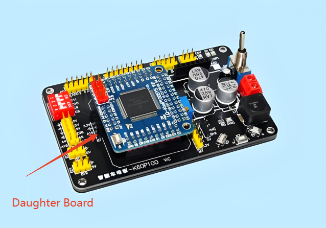
Standardization improves compatibility, reduces the chance of pin mismatch, and simplifies replacement in the future. Below is a typical daughter board picture and its internal parts:
8. Document Everything
Lastly, create full documentation before production. This should include:
Schematic diagram
Bill of materials (BOM)
Gerber files and drill files
Assembly drawings and 3D models
Test procedure, if applicable
Proper documentation ensures that your manufacturer and QA team can assemble and verify the board without confusion.
How EBest Circuit (Best Technology) Helps You?
When you’re developing daughter board PCBs, you want a manufacturing partner who understands your needs. EBest Circuit (Best Technology) brings reliability, fast lead times, and engineering support to every order. We provide professional design reviews for daughter board projects. Our engineers can help verify your connector choices, check your layout for manufacturability, and guide you in selecting cost-effective materials. We also offer PCB prototyping and small-batch PCB production so you can test your design before full rollout. Here’s how we help:
One-stop PCB services: From layout to fabrication and assembly.
Design guidance: Connector selection, board outline, and thermal layout advice.
Full component traceability during production.
Fast prototyping and volume production: Short delivery times with stable quality.
Competitive pricing: Transparent quotes with no hidden fees.
With rich experience in daughter board manufacturing, we support applications in medical, automotive, industrial, and more.
If you’re planning your next daughter board PCB project, feel free to contact us for expert advice and a free quote.
FAQs
1. Can I reuse daughter boards across different systems?
If the interface and power requirements match, you can often reuse them. That’s one of the big advantages of modular boards.
2. What connectors are best for daughter boards?
Common choices include board-to-board headers, card-edge connectors, and mezzanine sockets. The choice depends on current rating and mechanical space.
3. Can I order a prototype of my daughter board before full production?
Yes. EBest Circuit (Best Technology) offers quick-turn prototyping for testing and validation.
4. Do daughter boards need firmware?
Only if they contain microcontrollers or programmable components. Otherwise, they act as hardware extensions.
5. Is it possible to add a daughter board later after initial product release?
Yes. That’s the beauty of modular design—it allows upgrades or extensions without redesigning the main system.
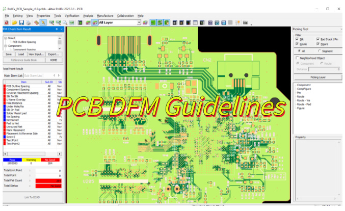
Why does PCB DFMmatter for reliable manufacturing? This guide covers design rules, layout strategies, and verification methods for optimized PCB production.
Does each engineering confirmation take 3-5 working days, slowing down the overall progress?
Do you know that more than 40% of the additional cost comes from process omissions in the design stage?
Can you afford the loss of the entire batch being scrapped due to undiscovered impedance deviation?
EBest Circuit (Best Technology) Can Provide:
Lightning DFM diagnosis: issue a 3D simulation report containing 267 process parameters in 12 hours (compared with peers in the industry in an average of 48 hours.
Cost sandbox simulation: use big data to predict the utilization rate of the board material, helping you save 8-15% of material loss.
Free engineering service: 24-hour online engineers answer your questions and avoid impedance deviation.
Welcome to contact us if you have any request for PCB design: sales@bestpcbs.com.
What Is PCB DFM?
PCB DFM(Design for Manufacturability) is a proactive approach to circuit board development that ensures designs can be efficiently and reliably manufactured. It involves analyzing layout elements such as trace widths, component spacing, via placement, and material choices to align with production capabilities while maintaining electrical performance.
By implementing DFM principles, designers avoid common pitfalls like insufficient solder mask clearance or unrealistic drill hole sizes that could lead to fabrication defects. The methodology also considers assembly requirements, ensuring proper thermal relief and component orientation for automated soldering processes.
This systematic verification reduces prototyping iterations, lowers production costs, and improves yield rates by addressing potential issues before manufacturing begins. Industry guidelines provide standardized benchmarks for implementing these checks throughout the design workflow.
PCB DFM Guidelines
Adopting DFM principles ensures PCB designs align with production capabilities, reducing errors and costs. Below are actionable guidelines for optimized manufacturing:
1. Layout Planning
Maintain ≥0.15mm (6mil) clearance between copper features to prevent solder bridges.
Place high-speed/RF components away from noise sources (e.g., switching regulators).
Use standard aspect ratios (e.g., 1:1 for SMT pads) to simplify assembly.
2. Component Placement
Position polarized components (e.g., electrolytic capacitors) with clear orientation markers.
Group similar parts (resistors, capacitors) to minimize pick-and-place time.
Avoid placing tall components (e.g., connectors) near board edges to prevent handling damage.
3. Solder Pad Design
Follow IPC-7351B standards for pad sizes (e.g., 0.5mm pitch QFN pads: 0.3mm solder mask opening).
Extend thermal pads on power components (e.g., MOSFETs) to improve heat dissipation.
Add solder paste stencils with 1:1 aperture-to-pad ratios for fine-pitch parts.
4. Trace Routing
Use ≥0.15mm (6mil) trace width for signals and ≥0.2mm (8mil) for power lines.
Avoid acute angles (<90°) to prevent acid traps during etching.
Isolate analog/digital grounds with single-point connections.
5. Via Design
Limit via-in-pad usage to reduce solder wicking (use filled/capped vias for BGA escape).
Maintain ≥0.25mm (10mil) annular ring to ensure via reliability.
Keep via aspect ratio (hole diameter: board thickness) ≤1:6 for plating consistency.
6. Thermal Management
Add ≥1mm² copper pours under power components (e.g., voltage regulators).
Include thermal vias (0.3mm diameter, 1mm pitch) to connect top/bottom layer heat sinks.
Avoid placing vias in thermal pad regions to prevent solder voiding.
7. Drill File Accuracy
Specify drill sizes in increments of 0.05mm (e.g., 0.2mm, 0.25mm).
Use separate files for plated (PTH) and non-plated (NPTH) holes.
Include a drill chart with tolerances (e.g., ±0.05mm for ≤0.5mm holes).
8. Silkscreen & Marking
Place reference designators ≥0.5mm away from pads to avoid solder mask interference.
Use high-contrast ink for silkscreen (e.g., white on green solder mask).
Include polarity marks for diodes, LEDs, and electrolytic capacitors.
9. Design for Assembly (DFA)
Minimize component count by using integrated devices (e.g., PMICs instead of discrete regulators).
Align SMT and THT components on the same side to reduce reflow passes.
Avoid mixing lead-free and leaded solder processes without manufacturer approval.
10. File Output & Validation
Generate Gerber files in RS-274X format with layer-specific extensions (e.g., .GTL for top copper).
Include a fabrication drawing with board outline, cutouts, and special instructions.
Run DFM checks using software tools (e.g., Valor NPI) to flag errors.
PCB DFM Layout Optimization Strategies
Component Placement Methodology
Functional grouping: Cluster components by circuit function (power, analog, digital) with at least 100 mil spacing between groups
Assembly considerations: Maintain 50 mil clearance around all components for pick-and-place machines
Thermal management: Position heat-generating components (voltage regulators, power ICs) with 200 mil spacing and access to thermal vias
Connector placement: Locate all board-to-board connectors within 300 mil of board edges
Signal Routing Best Practices
Trace geometry: Use 45° angles with minimum 3x width radius for bend transitions
Impedance control: Maintain consistent 5 mil spacing for differential pairs and reference planes
High-current paths: Implement 20 mil minimum width for 1A current carrying capacity
Noise isolation: Separate analog and digital grounds with at least 50 mil gap
Manufacturing Enhancement Features
Via standardization: Use 8 mil/16 mil (hole/pad) via sizes throughout the design
Solder mask: Apply 4 mil expansion on all SMD pads with 2 mil web minimum
Fiducial markers: Place three 40 mil diameter markers in L-shape pattern
Test points: Include 32 mil diameter test points every 5-10 components
Documentation Standards
Silkscreen: Use 45 mil height fonts with 7 mil line width
Layer identification: Mark all layers with orientation indicators
Version control: Include datecode and revision near board edge
Assembly drawings: Provide 1:1 scale component location diagrams
Design Validation Process
Run DRC checks with 6 mil minimum spacing rules
Verify annular rings meet 5 mil minimum requirement
Cross-check against manufacturer’s capability matrix
EBest Circuit (Best Technology) offers complimentary PCB DFM analysis reports to streamline your manufacturing process. Our automated system performs comprehensive design verification, checking 200+ manufacturing parameters against industry standards. You’ll receive detailed feedback on component spacing, trace widths, via placement, and other critical factors within 24 hours. This free service helps identify potential production issues before fabrication, reducing costly redesigns and delays. Simply upload your design files to receive a customized report with actionable recommendations. Our analysis covers all major fabrication aspects while maintaining strict data confidentiality. Take advantage of this professional evaluation to optimize your PCB design for manufacturability. Contact us now to get a free PCB DFM report:sales@bestpcbs.com.
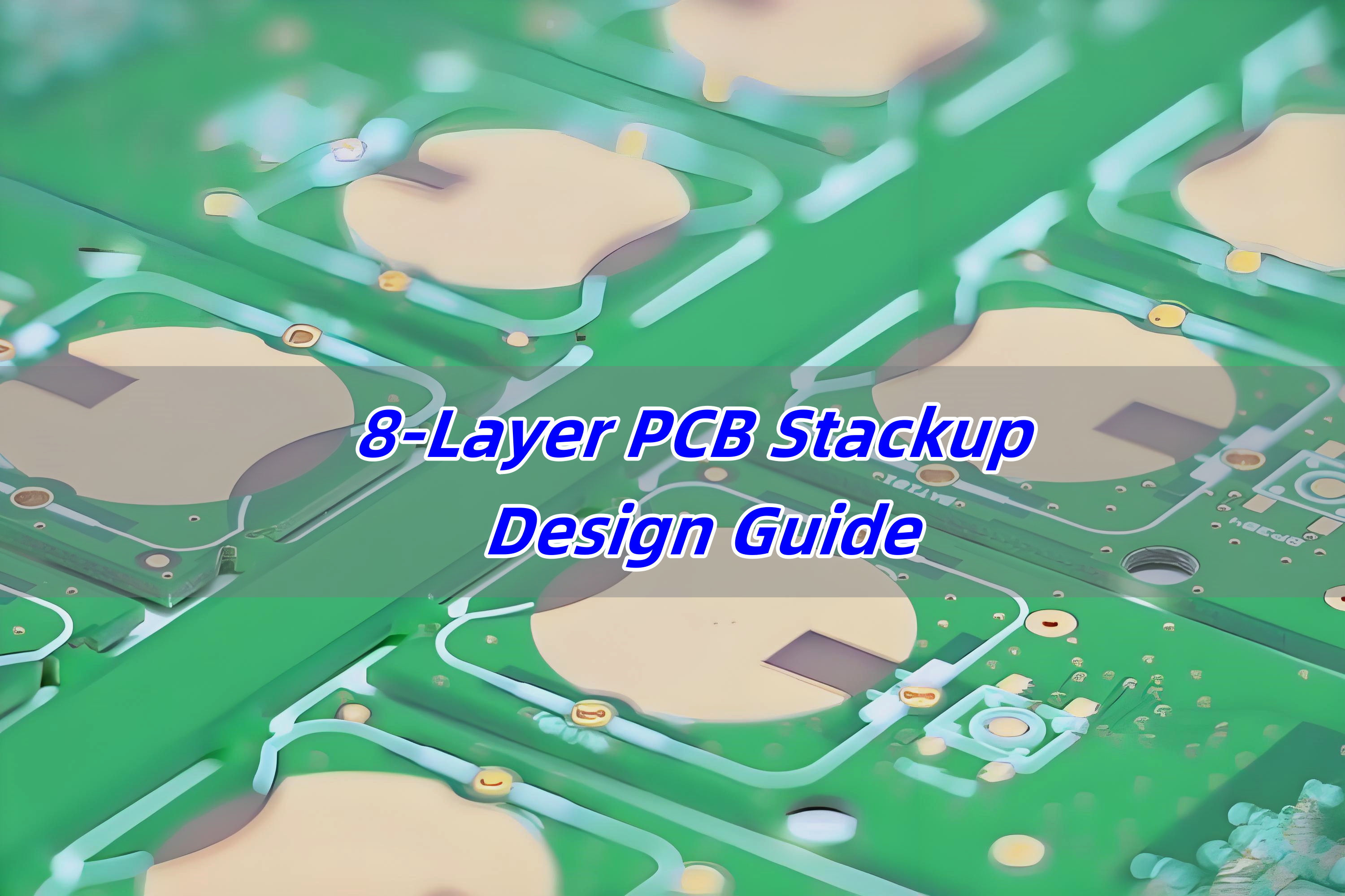
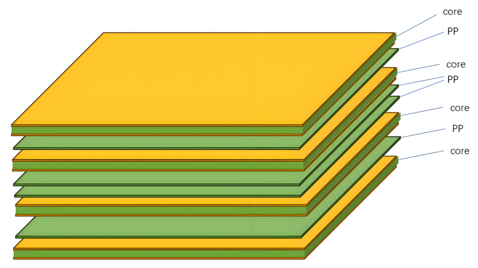
Designing a reliable multilayer circuit board starts with getting the stackup right. If your project involves high-speed signals, compact layouts, or reduced EMI, an 8-layer PCB stackup is a solid choice. It offers flexibility, better performance, and room for complex routing.
In this guide, we’ll walk you through everything you need to know—layer configurations, materials, sizes, and how to make the most of this structure with the help of a trusted PCB manufacturer.
What is a PCB Stackup?
A PCB stackup is the arrangement of copper layers and insulating materials inside a circuit board. These layers are stacked and bonded together using prepreg (resin-impregnated fiberglass) and core materials. The goal is to create a reliable board that supports both mechanical strength and excellent electrical performance.
In simple words, the stackup decides how signal layers, power planes, and ground layers are placed in the board. In high-speed digital designs, this structure plays a big role in signal quality, electromagnetic compatibility (EMC), and overall performance.
For an 8-layer PCB, the stackup consists of eight layers of copper with alternating dielectric materials. These are usually divided into four signal layers and four plane layers, though that can change based on your design needs.
PCB Stackup Considerations
For most PCB designs, there are often competing requirements between electrical performance, manufacturing limitations, cost targets, and system complexity. The final PCB stackup is usually a result of careful trade-offs across these factors. High-speed digital circuits and RF systems commonly rely on multilayer boards for better control and performance. Below are 8 essential principles to consider when designing a reliable stackup:
1. Layer Arrangement
In multilayer PCBs, you’ll typically work with signal layers (S), power planes (P), and ground planes (GND). Power and ground planes are usually solid, unbroken areas that provide low-impedance return paths for signal currents. Signal layers are often positioned between these planes to form symmetrical or asymmetrical stripline structures. The top and bottom layers are mainly used for component placement and limited routing. It’s best to keep traces on these outer layers short to reduce direct radiation and EMI.
2. Defining a Single Power Reference Plane
Decoupling capacitors are vital for maintaining power integrity, and they can only be placed on the outer layers of the PCB. The trace length, pad design, and vias connected to these capacitors greatly affect their effectiveness. To improve decoupling, make these connections short and wide, and minimize via length. For example, in a high-speed digital system, place decoupling capacitors on the top layer, dedicate the second layer to power for the processor, use the third layer for signal routing, and assign the fourth layer as a ground reference.
3. Incorporating Multiple Ground Planes
Using multiple ground planes helps create low-impedance return paths and minimizes common-mode EMI. Ground and power planes should be tightly coupled, and signal layers should also be close to reference planes. Reducing the dielectric thickness between layers improves coupling and enhances performance.
4. Managing Multiple Power Planes
When your design includes more than one power plane, these planes are often split into different voltage regions. If a signal layer is placed next to a multi-region power layer, signal currents may not find clean return paths, leading to noise or EMC issues. For high-speed digital signals, avoid routing traces near split power planes to prevent return current discontinuities.
5. Designing Signal Routing Pairs
When a signal travels from one layer to another, it creates what’s known as a “routing pair.” Ideally, the return current should stay within the same reference plane when switching layers. In practice, however, signals often need to transition between layers. To maintain signal integrity, ensure that return paths are available through stitching vias or decoupling capacitors. Using adjacent layers as routing pairs is a practical and effective strategy.
6. Routing Direction Guidelines
Keep trace directions consistent within each signal layer. At the same time, rotate the routing direction between adjacent signal layers. For instance, use horizontal routing (X-axis) on one layer and vertical routing (Y-axis) on the next. This practice reduces crosstalk and improves signal clarity.
7. Even-Layer Designs is Better
Although odd-layer PCBs may appear cheaper due to fewer materials, they’re more expensive to manufacture. That’s because odd-layer boards require non-standard lamination processes and additional handling steps. These increase the risk of surface damage, incorrect etching, and longer production times. In contrast, even-layer PCBs are more stable, cost-effective, and easier to produce at scale.
8. Budget
Multilayer PCBs are naturally more expensive than single- or double-layer boards. However, they offer significant benefits in functionality, miniaturization, EMI control, and signal integrity. When weighing total cost versus performance, the difference between multilayer and simpler boards may not be as high as expected.
Standard 8-Layer PCB Stackup Structure
When it comes to multilayer PCB design, the arrangement of signal, power, and ground layers directly affects signal integrity, EMI performance, and power delivery. Below are three common 8-layer stackup configurations, each with its own strengths and limitations.
Option 1:
Layer 1: Signal 1
Layer 2: Signal 2
Layer 3: Ground
Layer 4: Signal 3
Layer 5: Signal 4
Layer 6: Power
Layer 7: Signal 5
Layer 8: Signal 6
This layout alternates signal and power layers but does not take full advantage of the electromagnetic shielding benefits that a multilayer board can offer. The ground and power planes are separated, reducing the board’s EMI suppression capability. In addition, the power distribution network suffers from higher impedance, which may affect voltage stability in high-speed or high-current applications.
Option 2:
Layer 1: Signal 1
Layer 2: Ground
Layer 3: Signal 2
Layer 4: Power
Layer 5: Ground
Layer 6: Signal 3
Layer 7: Ground
Layer 8: Signal 4
This structure is widely regarded as the optimal 8-layer PCB stackup. It provides excellent electromagnetic shielding through the use of multiple ground planes. Each signal layer is placed adjacent to a reference plane (either ground or power), which improves signal stability and impedance control. Additionally, the tight coupling between power and ground planes enhances EMI performance and power integrity. This setup is ideal for high-speed, high-frequency, or noise-sensitive applications.
Option 3:
Layer 1: Signal 1
Layer 2: Ground
Layer 3: Signal 2
Layer 4: Power
Layer 5: Ground
Layer 6: Signal 3
Layer 7: Power
Layer 8: Signal 4
This configuration is a variation of Option 1 with improved EMI performance. By adding an extra reference plane, it provides better control over the characteristic impedance of the signal layers. However, the placement of the second power plane (with limited coupling to a nearby ground) leads to higher power delivery impedance, which could be a drawback in power-sensitive designs. Some optimization in power layer arrangement is still needed.
8-Layer PCB Stackup Materials
The performance of an 8-layer PCB stackup relies heavily on the materials used between and around its copper layers. These materials affect everything from electrical behavior to thermal stability and even mechanical strength. Let’s look at the two main categories: conductive and dielectric materials.
1. Conductive Layers
Copper is the most common metal used for the conductive layers in an 8-layer PCB. It’s highly conductive, easy to work with, and available in different thicknesses and finishes.
Copper Thickness: Most boards use ½ oz or 1 oz copper per layer. If the design needs to handle higher current, 2 oz or thicker copper may be used.
Copper Type: Standard copper foil is either electrodeposited (ED) or rolled. Rolled and annealed copper is smoother and more flexible, which makes it useful in boards that need better bend resistance.
Surface Finishes: The exposed copper is usually treated with a surface finish to protect it and ensure solderability. Options include HASL, ENIG, OSP, and immersion silver, among others.
2. Dielectric Layers
The dielectric materials are the insulating layers that separate the copper traces. These layers are critical for controlling impedance, heat flow, and electrical isolation.
FR-4: A glass-reinforced epoxy laminate, FR-4 is the most common dielectric for general-purpose PCBs. It’s reliable, widely available, and cost-effective.
High-Frequency Materials: For RF and high-speed digital designs, materials with low dielectric loss—like PTFE (Teflon), ceramic-filled PTFE, or hydrocarbon-based ceramics—are preferred. These support better signal integrity at high frequencies.
Thermal Conductive Materials: When heat dissipation is a concern, substrates like alumina or aluminum nitride are used. These materials offer higher thermal conductivity than standard epoxy systems.
To hold everything together, manufacturers use prepregs—uncured fiberglass sheets soaked in resin. Common prepreg materials include FR-4 for standard designs and polyimide for higher thermal or mechanical stress environments.
At the center of the stackup is the core, which acts like a spine for the board. This rigid layer typically uses FR-4 or polyimide, though in some high-power or high-heat applications, metal cores are added to improve thermal performance.
8-Layer PCB Thickness & Sizes
The total thickness of an 8-layer PCB depends on several factors:
Copper thickness: Common values are 0.5oz, 1oz, or 2oz per layer.
Prepreg/Core thickness: Adjusted to achieve specific impedance and board height.
Number of plane vs signal layers: Affects thermal and mechanical behavior.
Common Thickness Options:
1.6mm (0.063″) – Industry standard, suitable for most applications.
2.0mm to 2.4mm – Used when extra copper is needed for higher current.
3.2mm or custom – Selected for industrial or military-grade boards.
PCB Sizes:
Panel sizes are typically 18” x 24” before routing. Your board can be as small as a few millimeters or as large as the full panel, depending on the application.
6 Layer vs 8 Layer PCB
A 6-layer PCB consists of six layers of copper circuitry stacked with insulating layers (prepreg and core) in between. It usually includes:
4 Signal Layers for routing high- and low-speed signals
1 Power Plane to distribute voltage
1 Ground Plane to provide a return path and help with EMI suppression
A typical 6-layer stackup looks like this:
Layer 1: Signal (Top)
Layer 2: Ground
Layer 3: Signal
Layer 4: Signal
Layer 5: Power
Layer 6: Signal (Bottom)
While both 6-layer and 8-layer PCBs are widely used in advanced electronics, they serve slightly different purposes depending on design complexity, signal speed, and EMI requirements. Let’s compare them together:
Aspect
6-Layer PCB
8-Layer PCB
Layer Count
6
8
Typical Configuration
4 signal layers + 1 power + 1 ground
4 signal layers + 2 power + 2 ground
Routing Space
Moderate
More routing room
Signal Integrity
Good, suitable for most mid-speed signals
Excellent, supports very high-speed signal routing
EMI Shielding
Limited shielding with fewer ground planes
Strong EMI control due to multiple ground planes
Power Distribution
Single power plane, higher impedance
Dual power planes, better PDN performance
Design Complexity
Less complex, easier to design and fabricate
More complex, better for advanced designs
Thermal Performance
Adequate for medium power applications
Better heat spreading for high-power components
Cost
Lower fabrication cost
Higher cost due to more layers and materials
Use Case
Mid-level MCUs, general embedded, basic RF
FPGAs, DDR memory, high-speed data buses, complex SoCs
Use a 6-Layer PCB if:
Your design isn’t extremely dense.
The signals don’t require tight EMI control.
You want to balance performance and cost.
There’s no strict need for multiple ground or power planes.
It’s widely used in commercial electronics that don’t involve ultra-high-speed communication or compact multilayer routing challenges.
Choose an 8-Layer PCB when:
High-speed signals (such as PCIe, USB 3.x, DDR4, or SERDES) are involved.
EMI performance is critical, especially in sensitive industrial or medical devices.
You need more space for routing due to a denser component layout.
Stable power delivery is required across multiple voltage domains.
You’re working with a compact form factor that demands vertical signal distribution.
An 8-layer stackup allows designers to pair every signal layer with a nearby ground or power plane, which significantly improves signal quality and reduces noise.
Benefits of Working with an Experienced PCB Manufacturer
Designing and fabricating an 8-layer PCB stackup requires precise engineering and process control. Partnering with a reliable manufacturer like EBest Circuit (Best Technology) brings several benefits:
1. Stackup Design Assistance: Professional help with impedance control, signal integrity, and EMC optimization.
2. Material Expertise: Guidance in choosing suitable laminates for your specific requirements.
3. Advanced Fabrication: Capability to handle HDI, blind/buried vias, and tight tolerances.
4. Quality Assurance: Rigorous testing like AOI, X-ray, and impedance measurement.
5. Fast Turnaround: Efficient production process without sacrificing quality.
Why Choose EBest Circuit (Best Technology) for Your 8-Layer PCB Stackup?
EBest Circuit (Best Technology) is a trusted 8-layer PCB stackup specialist serving global customers across aerospace, medical, automotive, and industrial electronics. We hold certifications including:
ISO9001 for quality control
ISO13485 for medical electronics
IATF16949 for automotive-grade PCBs
AS9100D for aerospace applications
Our engineers assist with DFM check, impedance control, EMI reduction, thermal management, and material choices, ensuring your 8-layer design performs reliably under real-world conditions.
FAQs
1. What is the best layer configuration for an 8-layer PCB stackup?
A balanced configuration like Signal–GND–Signal–Power–GND–Signal–Power–Signal is often preferred for signal integrity and EMI control.
2. How much does an 8-layer PCB cost?
Cost varies by material, size, copper weight, and complexity, but typically ranges from $50 to $300 per board in small batches.
3. What software is used for 8-layer PCB design?
Tools like Altium Designer, Eagle, KiCAD, and OrCAD support multilayer PCB stackup planning and layout.
4. Can you use HDI features in 8-layer PCBs?
Yes. Blind and buried vias, via-in-pad, and microvias are often used in 8-layer HDI designs.
5. How do I choose the right manufacturer for 8-layer PCBs?
Look for certifications, material options, engineering support, and experience with multilayer stackups—like what EBest Circuit (Best Technology) provides.
Gold fingers are one of the most critical features in many circuit boards, especially those used in high-reliability connections. Whether you’re building a test interface, designing a PCIe card, or creating an edge connector, understanding gold finger beveling and its plating design is essential for durability and smooth performance.
Let’s explore everything about PCB gold fingers, the beveling process, and how to choose the right beveling angle for your board design.
What Is a Gold Finger?
PCB gold fingers are the gold-plated connectors located along the edge of a printed circuit board. They serve as contact points when a PCB is inserted into a slot or connector, just like in RAM, GPU cards, or other modular systems. These fingers are plated with hard gold to ensure they can withstand repeated insertion and removal cycles without wearing out.
They are called “fingers” because they look like narrow, elongated pads stretching along the PCB’s edge, similar to the fingers of a hand. Each gold finger connects to a circuit trace inside the board. When the PCB is inserted into a slot, the metal contacts on the gold fingers align with the contacts inside the connector, allowing signals to pass through.
The main reason gold is used is because it doesn’t corrode easily. Gold provides high conductivity and can withstand many insertions without losing its shape or functionality. In critical environments—like military, aerospace, or telecom—this reliability is essential.
Types of Gold Fingers in PCB
PCB gold fingers can be divided into two types – graded gold fingers and staggered gold fingers.
Graded Gold Finger
Graded gold fingers refer to a design where the fingers are plated with gold at varying lengths or staggered elevations. Instead of all the fingers being aligned in a straight line, some are slightly longer than others. This is not just a visual variation—it serves a very specific purpose. Graded fingers are typically used in applications where controlled insertion sequencing is required. When the PCB is inserted into the slot, the longer fingers make contact first, followed by the shorter ones.
Staggered Gold Fingers
Another design strategy is using long and short gold fingers—also known as staggered gold fingers. This refers to gold fingers of different physical lengths on the same board edge, but typically without beveling or plating depth variation. This technique is commonly used in:
PCIe hot-pluggable cards
Industrial control systems with replaceable modules
Burn-in or test fixtures requiring safe first-contact
The lengths are designed based on the depth of the connector slot and how the PCB enters the socket. Sometimes only a few pins—such as GND or VCC—are made longer, while the rest remain short.
How Thick Is PCB Gold Finger Plating?
The durability of gold fingers comes from their plating thickness. Not all gold fingers are created equal. The thickness of the plating affects both how well they perform and how long they last.
The gold layer is not pure; it is electroplated hard gold, which includes a bit of cobalt to improve hardness and wear resistance. Here’s a breakdown of common thicknesses:
Application Type
Gold Plating Thickness (Hard Gold)
Standard Consumer Devices
0.76μm (30μin)
Industrial or Light Insertion
1.27μm (50μin)
High-Durability Applications
2.54μm (100μin)
In general, 50μin is the most common for boards that are plugged and unplugged many times. If the fingers are not meant to be removed often, thinner plating is usually fine. But when in doubt, thicker is better—it provides stronger wear resistance.
What Is the Process of Gold Plating in PCB?
Creating strong, reliable pcb gold fingers requires precision. The plating process is done after the rest of the board is fabricated and cleaned. The focus is to add a hard gold layer only to the fingers—nowhere else. Here’s how the PCB gold finger plating process works step-by-step:
1. Finger Area Isolation
First, the PCB is cleaned, and only the finger areas are exposed. The rest of the board is masked to prevent unwanted plating elsewhere.
2. Nickel Plating (Bottom layer)
A nickel layer (typically 3–6μm) is electroplated onto the copper finger base. Nickel improves gold adhesion and acts as a barrier to prevent copper from diffusing into the gold over time.
3. Gold Electroplating (Top Layer)
After nickel, a layer of hard gold is plated on top. This layer is usually between 30μin and 100μin depending on the application. The plating uses a current that drives gold ions onto the nickel surface.
4. Cleaning and Inspection
Once the plating is complete, the board is cleaned, and the gold fingers are inspected for uniformity, roughness, or any missing areas.
5. Beveling (If Required)
If beveling is needed, it is done after plating. The edge is shaped to allow easier insertion into connectors.
6. Final Finishing
The rest of the PCB receives its finish (e.g., ENIG, OSP, HASL), but gold fingers remain untouched.
This plating method results in durable, smooth connectors that resist oxidation and mechanical wear.
What Is Gold Finger Beveling?
Gold finger beveling is a mechanical process that trims the edge of the PCB—where the gold fingers are located—into a sloped angle. Rather than a blunt 90° edge, the bevel creates a smooth ramp-like surface.
Imagine sliding a PCB into a connector. A sharp edge might catch, damage the connector, or scrape off the plating. But a beveled edge slides in smoothly, reducing friction and improving contact.
This is especially useful for PCBs used in:
Backplane systems
Server racks
Communication modules
Plug-and-play components
The beveling process is typically done using precision grinding or CNC milling. Care is taken to maintain exact angle measurements without overcutting the gold plating.
Purpose of Gold Finger Beveling
There are several important reasons why beveling is applied to PCB gold fingers:
Easier Insertion
A beveled edge helps the PCB slide into the connector smoothly. It reduces the chance of misalignment or jamming.
Prevents Contact Damage
Without beveling, the sharp PCB edge can scratch the connector pins, causing early wear or performance issues.
Reduces Wear and Tear
Repeated insertion cycles can wear out the gold plating. Beveling distributes the pressure more evenly, extending the lifespan of both board and connector.
Better Electrical Contact
Smoother insertion means better alignment and tighter contact with the metal pins inside the slot. This leads to more stable signals and fewer connection errors.
Professional Manufacturing Finish
Beveled gold fingers look more refined, signaling high-quality PCB craftsmanship.
For any board that’s going to be removed and reinserted frequently, beveling is not just a good idea—it’s almost essential.
Gold Finger Beveling Angle Options
When beveling, you have options for the bevel angle. The choice depends on how the PCB fits into its slot and the degree of insertion force you want to reduce. Here are the common beveling angles:
Angle
Description
30°
The most popular angle. Balances mechanical strength and ease of insertion.
40°
Offers a smoother slope than 30°. Used when insertion needs to be gentle.
45°
The steepest slope. Useful when the board must glide into the slot with minimal resistance.
Most applications stick with 30°, but you should always check the connector specification. Some high-density or high-speed connectors might require tighter tolerances and smoother entry paths.
Considerations of Beveling Angles
Before you finalize your beveling angle, consider the following:
Slot Geometry
Look at how your connector or socket is shaped. If the slot opening is narrow, a steeper bevel (like 45°) might be helpful.
Insertion Frequency
If the PCB will be removed often—like in test or modular setups—a smoother entry reduces long-term damage.
Mechanical Strength
Sharper bevels remove more material. If your board edge carries mechanical load, avoid overly steep bevels.
Gold Coverage
The beveling process should never cut through the gold. Make sure the gold plating thickness is enough to cover the entire bevel.
IPC Guidelines
Refer to IPC-6012 and IPC-A-600 for guidelines on gold finger design, plating, and beveling requirements.
Always coordinate with your PCB manufacturer to ensure the chosen bevel angle is feasible and matches your product’s functional needs.
PCB Gold Fingers Applications
Gold fingers are everywhere. Any device that uses edge connectors likely has them. Some of the most common use cases include:
Graphics cards (GPU) – for connecting with the motherboard
RAM modules – inserted into DIMM slots
Motherboards and backplanes – for communication between layers or devices
Test interface boards – for burn-in, programming, or debugging
PLC and industrial control systems – for module plug-in
Medical and defense electronics – where reliability is critical
In all these applications, gold finger beveling helps ensure the boards don’t fail during connection or removal. It may seem like a small detail, but its effect on reliability is huge. Gold finger beveling is one of those small but powerful features that improves the mechanical fit, electrical contact, and overall durability of your circuit boards. When designing your next PCB, pay attention to:
The gold finger plating thickness
Whether beveling is needed
The best angle for smooth insertion
And the wear-and-tear the board will experience
These decisions affect not only how well the board works, but how long it lasts.
About EBest Circuit (Best Technology)
At EBest Circuit (Best Technology), we specialize in PCB manufacturing with a focus on high-reliability boards. We handle everything from custom hard gold finger design to precision beveling, ensuring your edge connectors meet international standards. Our team works with industries including medical, automotive, aerospace, and telecom.
We follow strict quality processes and use MES traceability systems to track every step. Whether you need quick prototypes or high-volume production, our engineers are ready to help you design, test, and deliver high-performance PCBs with durable gold fingers.
Looking for a PCB manufacturer that understands the details? Let’s build your next project together.
FAQs
1. Can I design gold fingers without beveling?
Yes, but for any board that will be plugged in and out regularly, beveling is highly recommended for smoother insertion and longer lifespan.
2. What’s the difference between ENIG and hard gold?
ENIG is used on pads for soldering. Hard gold is plated on fingers for wear resistance. They are different in composition and use.
3. How do I specify beveling on my Gerber files?
You should include a separate mechanical drawing or notation in the fabrication notes to indicate the beveling angle and location.
4. Are gold fingers more expensive to produce?
Yes, due to the electroplating process and gold material cost. However, they add significant durability and value.
5. Can gold finger plating wear off?
Over time, yes—especially if the plating is thin. Using thicker plating like 50μin or more helps prevent this.
Rogers RO4350B is one of the most popular PCB materials used in high-frequency applications today. If you’re designing circuits that need stable performance at GHz-level speeds, this material often stands out. In this blog, we’ll explore what RO4350B is, what it’s made of, available thicknesses, and why it’s preferred over other materials for high-frequency PCB designs.
What Is Rogers RO4350B Material?
RO4350B is a type of high-frequency laminate developed by Rogers Corporation. It’s engineered for performance in RF (radio frequency) and microwave applications, offering superior electrical characteristics compared to standard FR-4. Unlike generic epoxy-based materials, RO4350B uses a hydrocarbon-ceramic composition that keeps signal losses low even at high frequencies.
This material combines the electrical performance of PTFE (commonly used in high-end RF applications) with the manufacturability of FR-4, making it a cost-effective and reliable choice for high-speed designs.
What Is Rogers Material Made of?
Rogers materials, including RO4350B, are made from hydrocarbon resins with ceramic fillers and reinforced with woven glass. This composite structure delivers excellent mechanical stability and consistent dielectric properties.
Unlike traditional PTFE-based laminates, Rogers materials like RO4350B do not require special handling during PCB fabrication, which saves both time and cost. Rogers materials are engineered to balance electrical performance with ease of manufacturing, which is essential when producing high-frequency PCBs at scale.
RO4350B Dielectric Constant
The dielectric constant (Dk) is a critical factor in high-frequency PCB materials, as it affects signal speed and impedance control. The RO4350B dielectric constant is typically 3.48 ± 0.05 at 10GHz, which is both stable and predictable over a wide range of frequencies and temperatures.
The consistency of frequencies and temperatures ensure that transmission lines behave as expected, which is especially important in RF circuits, microwave devices, and antenna structures. Stable Dk also simplifies impedance control and reduces the risk of signal reflection and distortion.
What Is the Standard RO4350B Thickness?
RO4350B PCBs are available in multiple standard thicknesses to meet different design and performance requirements. Common options include:
0.254 mm (10 mil)
0.508 mm (20 mil)
0.762 mm (30 mil)
1.524 mm (60 mil)
These thicknesses allow designers to select the best stack-up for impedance control, thermal dissipation, and mechanical strength. Depending on your signal layer, ground layer spacing, or copper weight, one of these thicknesses will likely align with your project’s needs.
RO4350B Datasheet
Before choosing a material for your RF or high-speed digital PCB, it’s essential to understand the technical specifications. Here is a summary of the most important values from the RO4350B datasheet:
Property
Typical Value
Test Condition / Note
Dielectric Constant (Dk)
3.48 ± 0.05
@ 10 GHz (z-axis)
Dissipation Factor (Df)
0.0037
@ 10 GHz
Volume Resistivity
1.7 × 10⁸ MΩ·cm
ASTM D257
Surface Resistivity
4.4 × 10⁷ MΩ
ASTM D257
Electrical Strength
>800 V/mil
ASTM D149
Dielectric Breakdown
>40 kV
ASTM D149
Thermal Conductivity
0.69 W/m·K
ASTM D5470
Coefficient of Thermal Expansion (CTE)
11 ppm/°C (x, y) / 32 ppm/°C (z)
-55°C to 288°C
Glass Transition Temperature (Tg)
>280°C (no defined Tg)
Thermomechanical analysis
Decomposition Temperature (Td)
~425°C
TGA method
Solder Reflow Resistance
Excellent
No delamination or blistering
Tensile Modulus
1.4 × 10⁶ psi (x-y)
ASTM D638
Flexural Strength
20,000 psi (typical)
ASTM D790
Peel Strength
≥1.1 N/mm
IPC-TM-650
Young’s Modulus
~10 GPa
Estimated from stress-strain curve
Moisture Absorption
0.06%
ASTM D570
Density
1.86 g/cm³
ASTM D792
Flammability Rating
UL 94 V-0
UL 94
Water Absorption
<0.1%
Excellent water resistance
Material Composition
Ceramic-filled hydrocarbon resin + glass fiber
Non-PTFE-based
Halogen-Free
Yes
RoHS & REACH compliant
Available Copper Foil
0.5 oz, 1 oz, 2 oz (18µm, 35µm, 70µm)
Rolled and electro-deposited options available
If you need the full official datasheet in PDF format, you can also request it from EBest Circuit (Best Technology) along with a quote for your project.
How Much Does Rogers PCB Cost?
Compared to FR-4, the rogers RO4350B price is higher due to its premium performance. On average, RO4350B material can cost between $8 to $25 per square foot, depending on thickness, copper weight, and supplier volume. Full PCB fabrication using RO4350B typically results in a 20–50% higher price than using standard FR-4, mainly due to the material cost and additional processing steps.
However, when you’re working with high-frequency applications—such as 5G, radar, or satellite communications—the improved signal integrity and reduced loss often justify the added cost.
What Is the Difference Between RO4003 and RO4350B?
Both RO4003 and RO4350B are part of Rogers’ high-frequency laminate series, but they have subtle differences:
Feature
RO4003C
RO4350B
Dielectric Constant
3.38
3.48
Loss Tangent
0.0027 @ 10 GHz
0.0037 @ 10 GHz
Flame Rating
Non-UL rated
UL 94 V-0
Cost
Slightly lower
Slightly higher
Process Compatibility
Standard PCB process
Standard PCB process
RO4003 is better suited for applications where cost sensitivity is critical and UL rating is not required. RO4350B, on the other hand, provides a better flame rating and slightly improved mechanical properties, so it is the preferred choice for commercial or defense-grade applications.
Why Choose RO4350B as High Frequency PCB Material?
High frequency PCB, also known as RF PCB, refers to a special circuit boards with relatively high electromagnetic frequencies. This PCB is mainly used in the fields of high frequency (>300 MHz or wavelengths <=1 meter) and microwaves (>3 GHz or wavelengths <= 0.1 meter). If you’re designing a high-frequency PCB, choosing RO4350B gives you the best of both worlds: high performance and ease of fabrication. Here’s why many engineers choose this material:
Low dielectric loss helps reduce signal attenuation.
UL 94 V-0 flame resistance, which is crucial for safety.
Compatible with standard FR-4 processing, so no need for Teflon-specific tooling.
All of these feature help maintain signal quality in applications like RF transmitters, satellite receivers, and high-speed digital circuits. So even if the RO4350B price is slightly higher, it’s often more cost-effective than debugging performance issues caused by suboptimal materials.
High Frequency PCB Design Guidelines
When working with RO4350B PCB material, keep the following design practices in mind to get the best results:
1. Control impedance: Use proper stack-up and trace width calculators for accurate 50Ω or 75Ω routing.
2. Minimize vias: Each via introduces inductance and can distort signals at high frequencies.
3. Short trace lengths: High-speed signals should have the shortest possible paths.
4. Proper grounding: Always include a continuous ground plane to reduce EMI and improve return paths.
5. Avoid sharp corners: Use 45-degree or curved traces instead of 90-degree angles.
6. Use differential pairs: For high-speed interfaces like USB or LVDS, tightly coupled pairs reduce crosstalk and maintain signal integrity.
Combining these techniques with the natural performance of RO4350B helps you unlock superior RF performance without increasing fabrication complexity.
Why EBest Circuit (Best Technology) Is Your Reliable RF PCB Manufacturer?
At EBest Circuit (Best Technology), we specialize in high-frequency PCB manufacturing using premium materials like RO4350B, RO5880, RO4003C. With ISO-certifications, we’re equipped to serve industries ranging from automotive and medical to aerospace and communications. Whether you’re developing high-reliability prototypes or large-scale production, you can count on us as your reliable one-stop PCB & PCBA partner.
We offer:
Strict impedance control with advanced test equipment
Rapid prototyping and flexible volume production
Competitive RO4350B price with guaranteed traceability
Expert engineering support for layout and material selection
No MOQ requires, 1 piece available also
5 years quality guarantee, free rework and functional testing
Free DFM check
If you’re looking to manufacture reliable high-frequency PCBs, you’re in the right place.
FAQs
1. Is RO4350B suitable for multilayer PCBs?
Yes, RO4350B is commonly used in multilayer designs for RF and microwave applications. It offers stable performance in both single and multi-layer stack-ups.
2. How does RO4350B perform at 5GHz or higher?
It maintains low loss and consistent Dk values even at frequencies above 5GHz, making it reliable for 5G and radar circuits.
3. Can RO4350B be used with FR-4 in hybrid stack-ups?
Yes, it can. Many engineers use RO4350B for RF layers and FR-4 for power/control layers to reduce cost.
4. What is the shelf life of RO4350B material?
Stored under proper conditions, it has a long shelf life—typically over a year without degradation.
5. Do I need special PCB fabrication for RO4350B?
No. Unlike PTFE-based materials, RO4350B is compatible with standard PCB fabrication processes, which simplifies manufacturing.