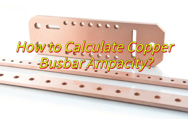
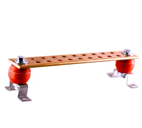
How to calculate copper busbar ampacity? This guide covers calculation methods, sizing charts (including 12x4mm), and comparisons with aluminum, providing datasheet for electrical system design.
Are you troubled with these questions?
- High electricity bills?
- Overheating issues?
- Slow custom orders?
EBest Circuit (Best Technology) can provide you service and solution:
- Save energy – 15% lower resistance, higher efficiency.
- Cooler operation – 20% better heat dissipation, longer lifespan.
- Faster delivery – 72-hour custom production, no delays.
Welcome to contact us if you have any request for copper busbar: sales@bestpcbs.com.
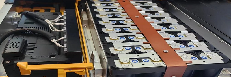
What Is Copper Busbar Ampacity?
Copper Busbar Ampacity refers to the maximum continuous current a copper busbar can safely carry under specific environmental conditions (e.g., temperature, heat dissipation, insulation level). It is determined by factors like cross-sectional area, copper purity, surface treatment, and installation methods (such as dense packing or ventilation).
How to Calculate Copper Busbar Ampacity?
Methods about how to calculate copper busbar ampacity:
1. Cross-Sectional Area Estimation (Single Busbar)
- Formula: I=W×K
- W: Busbar width (mm)
- K: Thickness factor (e.g., 18 for 10mm thickness)
2. Multi-Layer Busbar Correction
- Double-Layer: Idouble=Isingle×1.58
- Triple-Layer: Itriple=Isingle×2
3. Temperature Correction
- Lower Temperature (e.g., 25℃): Icorrected=I40×1.18
- Higher Temperature (e.g., >40℃):Icorrected=I40×0.9
4. Simplified Formula
- Formula: I=W×(T+8.5)
- W: Busbar width (mm)
- T: Busbar thickness (mm)
5. Environmental & Installation Adjustments
Parallel Busbars (AC):
- 2 bars: I×0.8
- 3 bars: I×0.7
- 4 bars: I×0.6
6. Copper vs. Aluminum Conversion
Formula: Icopper=Ialuminum×1.3
7. Practical Recommendations
- Refer to Tables: Use standards like Industrial and Civil Power Distribution Design Manual for precision.
- Safety Margin: Design with 10–20% reserve capacity.
- Temperature Monitoring: Ensure long-term temperature rise ≤70K (Class F insulation) to prevent aging.
What is the Ampacity of a 12 x 4 Copper Busbar?
For a 12×4mm copper busbar (40℃ ambient, ΔT≤50K):
- Vertical mounting: ~320A (bare copper).
- Horizontal mounting: ~280A (12% reduced heat dissipation).
Key adjustments:
- Tin-plated surface: +8% (→345A vertical).
- 60℃ ambient: Derate 30% (→~224A).
Copper Busbar Ampacity Table in MM
| Busbar Size (Width × Thickness, mm) | Ampacity(Vertical, A) | Ampacity (Horizontal, A) | Horizontal Reduction Factor |
| 15 × 3 | 165 | 145 | 0.88 |
| 20 × 5 | 290 | 255 | 0.88 |
| 30 × 4 | 400 | 360 | 0.90 |
| 40 × 5 | 540 | 485 | 0.90 |
| 50 × 6 | 740 | 665 | 0.90 |
| 60 × 6 | 900 | 800 | 0.89 |
| 80 × 8 | 1,400 | 1,260 | 0.90 |
| 100 × 10 | 2,300 | 2,050 | 0.89 |
| 120 × 12 | 2,900 | 2,600 | 0.90 |
Copper Busbar DC Ampacity Chart
| Copper Busbar Dimensions (Width × Thickness, mm) | Single-Layer Ampacity (A) | Double-Layer Ampacity (A) | Triple-Layer Ampacity (A) |
| 40 × 4 | 480 | 750 | 960 |
| 60 × 6 | 840 | 1,344 | 1,722 |
| 80 × 8 | 1,280 | 2,000 | 2,560 |
| 100 × 10 | 1,810 | 2,824 | 3,620 |
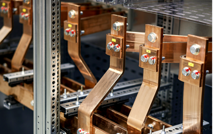
Copper vs Aluminum Busbar Ampacity
Conductivity & Ampacity
- Copper Busbar: Higher conductivity (58 MS/m). Ampacity ~1.43× aluminum for same dimensions. Supports 2-4A/mm².
- Aluminum Busbar: Lower conductivity (35-37.7 MS/m). Requires ~30% larger cross-section to match copper’s ampacity. Supports 3-5A/mm².
Physical Properties
| Parameter | Copper | Aluminum |
| Density | 8.9g/cm³ (3.3× aluminum) | 2.7g/cm³ |
| Thermal Expansion | 16.5ppm/°C | 23.1ppm/°C |
| Melting Point | 1,085°C | 660°C |
Mechanical Performance
- Copper Busbar: Higher strength, resistant to deformation/creep. Ideal for high-stress environments.
- Aluminum Busbar: Softer, prone to creep. Requires surface treatment (e.g., tin plating) to reduce contact resistance.
Cost & Weight
- Copper Busbar: 2-3× higher cost per ampacity unit. Heavier (3.3× aluminum).
- Aluminum Busbar: ~40% cheaper. Lightweight (1/3 of copper’s weight).
Environmental Adaptability
- Copper Busbar: Stable at high temps (40°C ampacity = 85% of 25°C). Low oxidation impact.
- Aluminum Busbar: Sensitive to temp rise (40°C ampacity = 70-85% of 25°C). Forms high-resistance oxides.
Safety & Application
- Copper Busbar: Higher melting point reduces arc risks. Critical for data centers/substations.
- Aluminum Busbar: Lower melting point increases arc hazards. Suitable for residential/light industry.
Trade-offs
- Copper Busbar: Compact, durable, high ampacity. Expensive, heavy.
- Aluminum Busbar: Cost-effective, lightweight. Requires larger size, frequent maintenance.
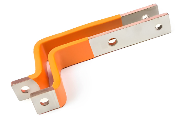
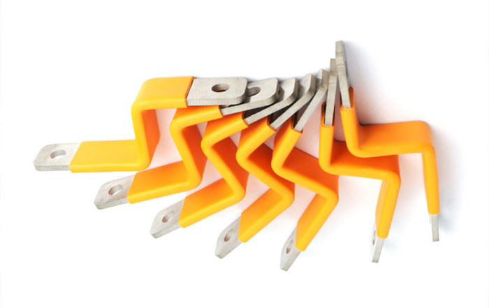
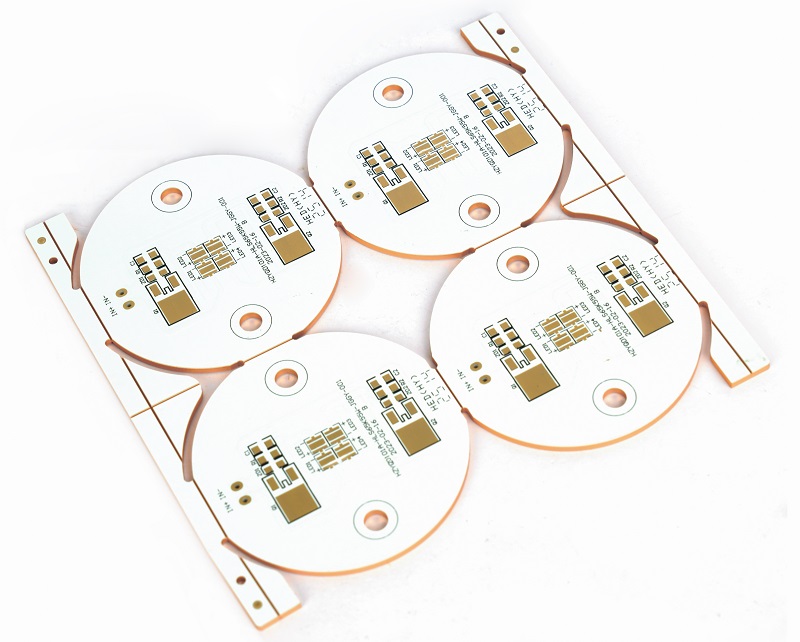
Why Choose EBest Circuit (Best Technology) as Copper Busbar PCB Manufacturer?
Reasons why choose us as copper busbar PCB manufacturer:
- Global Quality Certifications: ISO 9001 (quality management), ISO 14001 (environmental management).UL certification for flame resistance and current-carrying capacity.
- Competitive Pricing: Direct factory pricing with no middlemen, reducing costs by 15-20% compared to industry averages.
- Fast Lead Times: 24-hour prototype delivery for standard designs; 98% on-time delivery rate for bulk orders (500+ units).
- Premium Material Quality: Uses 99.9% purity copper (T2 grade) with third-party material certification.
- Advanced PCBA Integration: In-house SMT assembly lines supporting 0201 components and 0.3mm pitch BGAs.
- One-Stop Service: Covers design optimization → prototyping → mass production → PCBA assembly → testing.
- Rigorous QC Processes: 4-stage inspection: incoming material check → in-process monitoring → final electrical test → aging test.
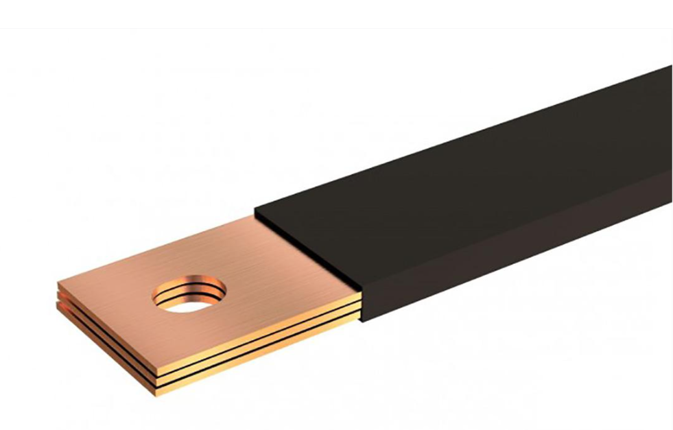
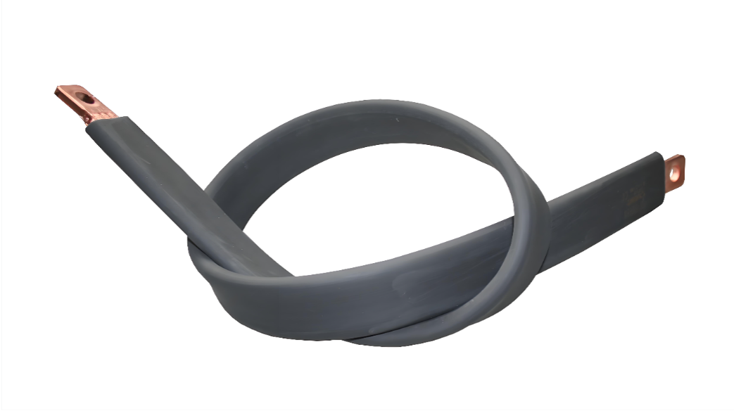
- Customization Flexibility: Supports multi-layer busbars (up to 6 layers) and complex geometries; Accepts small-batch orders (as low as 10 units) with no MOQ restrictions.
- Engineering Support: Free DFM (Design for Manufacturability) analysis to optimize cost and performance. And 24/7 technical support via email/phone for troubleshooting.

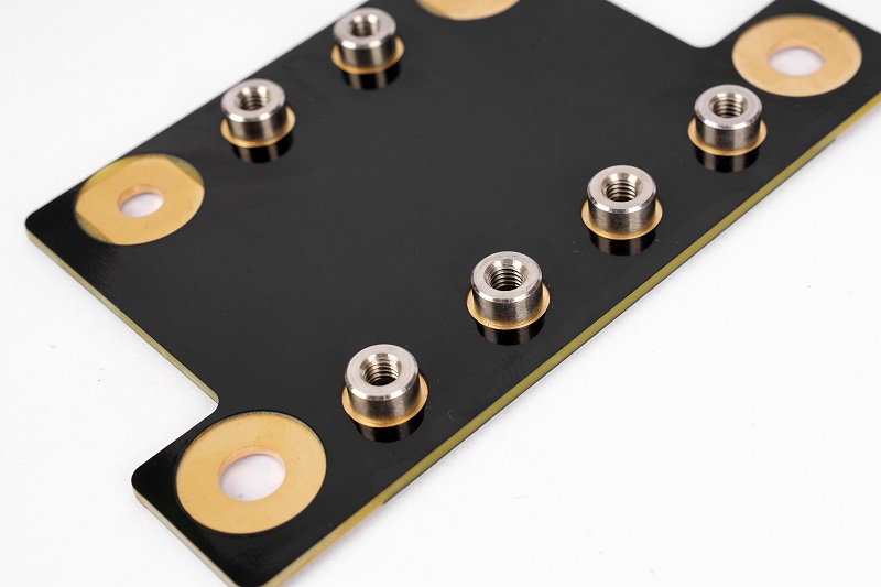
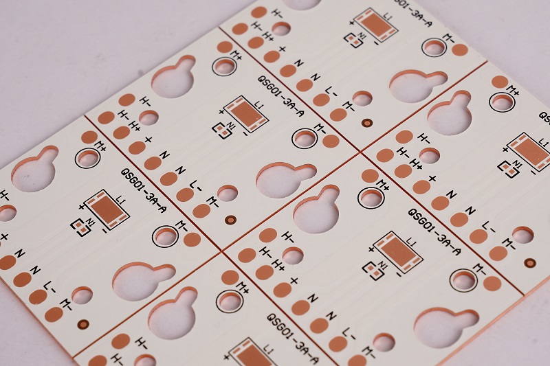
Our Busbar PCB Capabilities
| Parameter | Value/Description |
| Copper Bar Spacing | 0.8-1.0mm |
| Copper Thickness | 1.0mm-3.0mm |
| Current Carrying Capacity | 50-300A |
| Bendability | Customizable bending upon request |
| Surface Finishing Options | ENIG (Electroless Nickel Immersion Gold), Immersion Silver, Gold Plating |
| Board Thickness | 3.0-6.0mm |
| Hole Wall Thickness | ≥25μm |
| Aspect Ratio | 1:6 or 1:7 (for 1.0mm copper thickness with minimum 0.7mm hole diameter) |
| Layer Count | Typical 3-4 layers; additional layers require design evaluation |
| Maximum Dimensions | Standard: 600×400mm; Double-sided: 900×600mm |
| Lead Time | 3-4 layers: 13-15 days; add 3 days per layer beyond 4 layers |
How to Get A Quote For Copper Busbar PCB Project?
Materials Required for Accurate Quotation:
Design Files
- 2D CAD drawings (DXF/DWG) or 3D models (STEP/IGES).
- Cross-sectional busbar dimensions (width × thickness).
Technical Specifications
- Current rating (amps) and allowable temperature rise.
- Copper material grade (e.g., T2, C110).
- Surface finish requirements (e.g., tin plating, nickel).
Production Details
- Order quantity (prototypes/bulk).
- Lead time expectations (urgent/standard).
Additional Requirements
- Certifications (UL, RoHS).
- Special testing (e.g., hi-pot, thermal cycling).
- Packaging preferences (anti-static, custom boxing).
Welcome to contact us if you have any request for copper busbar PCB: sales@bestpcbs.com.