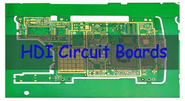
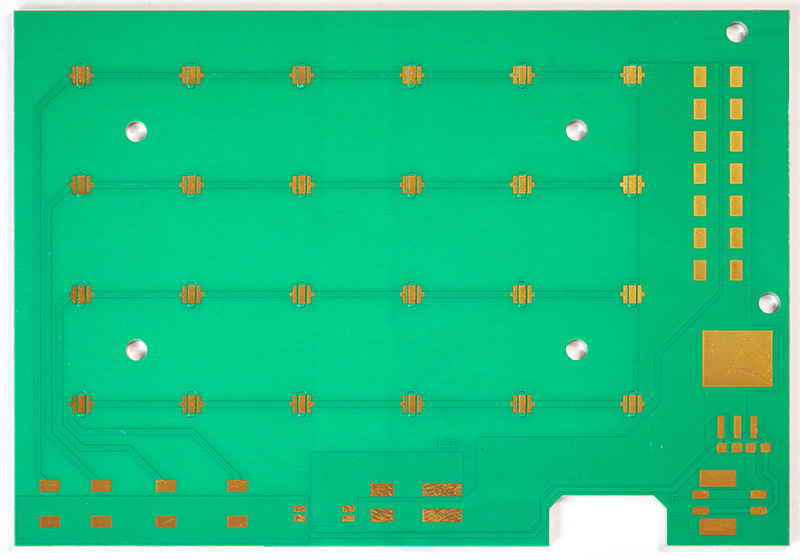
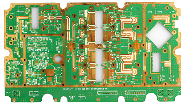
In RF, microwave, and high-speed digital engineering, DK and DF are two of the most important material parameters. They determine how fast signals propagate, how much loss occurs at higher frequency, and how clean your impedance remains across the entire channel. Whether you are building 5G radios, radar modules, mmWave sensors, or 28Gbps backplanes, understanding dk and df in PCB is essential.
This complete guide explains DK, DF, how they affect PCB performance, and how to choose materials for advanced designs.
What Is DK in PCB?
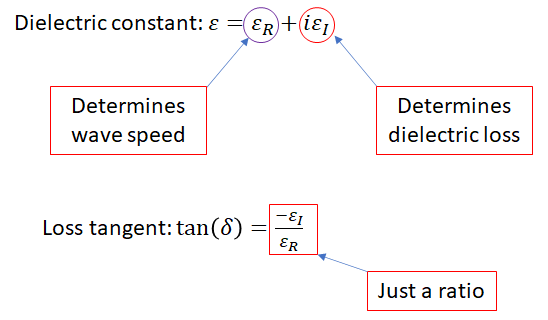
When engineers ask what is DK in PCB, they refer to the dielectric constant of the laminate material. DK tells us how much electric energy the material can store when a high-frequency signal travels through it.
- Higher DK → slower signal propagation
- Lower DK → faster signal propagation
The numeric value is important, but stability matters even more:
- DK must remain stable across temperature
- DK must remain stable across humidity
- DK must remain stable across frequency range
If DK shifts too much, the impedance changes. This causes timing errors, tuning drift, or degraded RF performance.
Why DK matters:
- Controls impedance for microstrip and stripline traces
- Influences signal delay and phase velocity
- Affects antenna tuning and RF filter accuracy
- Impacts coupling, resonant frequency, and trace dimensions
For radar, satellite RF, or 112Gbps SerDes, DK stability is critical.
What Is a Good DK Value for High-Frequency PCB Design?
A “good” DK depends on your application. Below are typical recommended DK ranges:
| Frequency Range | Suggested DK Range | Notes |
| 1–3 GHz | 3.2–4.5 | FR4 may still work for some designs |
| 3–10 GHz | 2.9–3.7 | Rogers RO4000 series is popular |
| 10–40+ GHz | 2.0–3.2 | PTFE, RO3000 series, Megtron materials |
Common examples:
- RO3003 (DK = 3.0) → excellent for RF/microwave/mmWave
- RO4350B (DK ≈ 3.48) → great for mixed RF + digital systems
- RT5880 (DK ≈ 2.2) → premium for mmWave (24–80 GHz)
Mid-range DK around 2.9–3.5 is ideal for most RF and high-speed digital designs.
What Is DF in PCB?
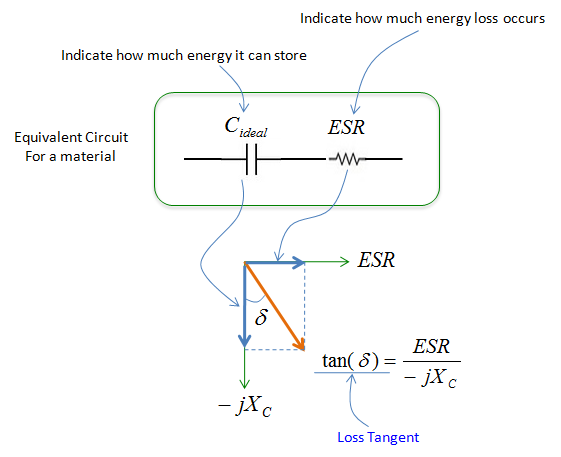
When engineers ask what is DF in PCB, they refer to the dissipation factor, also known as:
- loss tangent
- tan δ
- dielectric loss factor
DF shows how much of the signal energy turns into heat as it travels through the dielectric.
- Low DF → low loss → high-frequency performance is cleaner
- High DF → more loss → signals fade faster
DF matters more as frequency increases.
For example:
- FR4 DF ≈ 0.015
- RO3003 DF ≈ 0.001
- PTFE DF ≈ 0.0009
This small numeric difference creates a huge difference at 10 GHz or 28Gbps.
Why Does DF Impact Insertion Loss?
Total insertion loss comes from:
- Conductor loss
- Dielectric loss (directly tied to DF)
- Radiation loss
- Copper roughness
Higher DF means the dielectric absorbs more power, raising insertion loss and degrading signal integrity.
Effects of high DF:
- Closed eye diagrams at 10–28Gbps
- Significant attenuation in RF feedlines
- Reduced antenna efficiency
- Shorter allowable routing lengths
That’s why high-performance systems use materials like RO3003, PTFE, Megtron 6, or RO4350B.
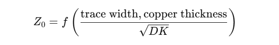
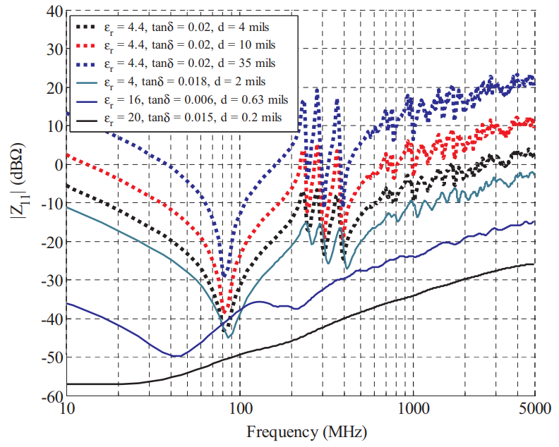
DK and DF in PCB Formula
Engineers often search for DK and DF in PCB formula to understand how materials influence signal behavior.
1. Phase Velocity

2. Dielectric Loss Approximation

3. Impedance Relation
- Higher DK → lower impedance
- Lower DK → higher impedance
These formulas guide stack-up planning and impedance modeling.
Why DK and DF Matter in PCB Design?
DK and DF are the foundation of RF and high-speed performance:
| Parameter | DK Influence | DF Influence |
| Impedance | Very strong | Minimal |
| Insertion loss | Moderate | Strong |
| Propagation delay | Strong | Minimal |
| RF matching | Strong | Moderate |
| Channel length limits | Low impact | Huge impact |
For high-speed digital circuits:
→ DF dominates, because loss determines signal integrity.
For RF/microwave circuits:
→ DK dominates, because it controls tuning and impedance.
For mmWave systems:
→ Both DK and DF must be extremely stable.
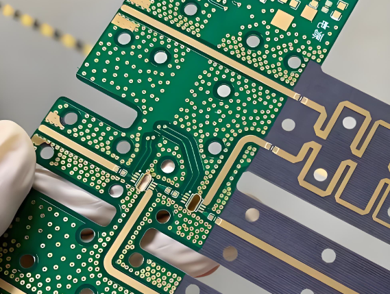
Typical DK and DF Values of Common PCB Materials
(Values at ~10 GHz; may vary by test method.)
| Material Type | DK | DF | Notes |
| Standard FR4 | 4.2–4.8 | 0.015–0.02 | Not suitable for >3–5 GHz |
| High-TG FR4 | 4.1–4.3 | 0.010–0.014 | Better stability |
| Rogers RO4003C | 3.38 | 0.0027 | Very popular RF material |
| Rogers RO4350B | 3.48 | 0.0037 | Mixed RF + high speed |
| Rogers RO3003 | 3.00 | 0.001 | Ultra-stable laminate |
| PTFE (Teflon) | 2.1–2.3 | 0.0009 | Ideal for microwave/mmWave |
| Megtron 6 | 3.3–3.7 | 0.002–0.003 | Excellent for 28G–112G SI |
| Ceramic-filled hydrocarbon | 2.9–3.5 | 0.0015–0.003 | Good for compact 5G modules |
How DK and DF Influence Impedance and Stack-Up Design?
1. Impact on Impedance
- Higher DK → narrower traces needed
- Lower DK → wider traces
Even tiny DK variations (±0.02) can change impedance significantly at GHz speeds.
2. Impact on Routing Length
- Higher DF → higher attenuation → shorter allowable trace lengths
- Lower DF → longer, cleaner channels
3. Impact on Layer Stack-Up
Stack-ups must account for:
- dielectric thickness stability
- resin/glass ratio
- copper roughness
- prepreg behavior
- weaves (spread vs standard)
A well-designed stack-up reduces tuning cycles and improves yield.
How to Choose the Right PCB Material for High-Speed & RF Projects?
Use these guidelines:
Below 3 GHz
- High-TG FR4 often acceptable
3–10 GHz
- Rogers RO4003C
- Rogers RO4350B
- Panasonic Megtron 4
10–40+ GHz
- RO3003
- RO3035
- RT5880
- PTFE-based laminates
- Megtron 6 or Megtron 7 for digital
Consider these factors:
- Required bandwidth
- Acceptable insertion loss
- Channel length
- Operating temperature
- Fabrication constraints
- Material availability
DF < 0.003 is recommended for mmWave or 28Gbps+ channels.
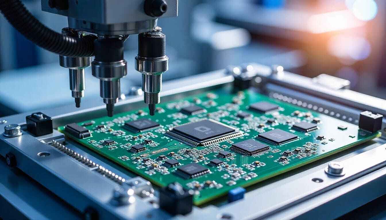
EBest Circuit (Best Technology) provides stack-up design, DFM review, material selection support, and impedance simulations to ensure successful builds.
FAQs About DK and DF in PCB
1. Are DK and dielectric permittivity the same concept?
Yes. DK is the relative permittivity. Datasheets express it as DK because it directly relates to PCB performance.
2. Does copper roughness influence DK/DF performance?
Yes. Rough copper:
- Increases conductor loss
- Raises effective DK
- Degrades high-frequency performance
Smooth copper (e.g., reverse-treated) improves SI and RF behavior.
3. Which materials offer the lowest DF for mmWave PCB builds?
- PTFE composites
- Rogers RO3003
- Rogers RO3035
- RT/duroid 5880
These materials support 24–80 GHz mmWave designs.
4. How do I read DK and DF on a laminate datasheet?
Check:
- Frequency of measurement (must match your design)
- Test method (IPC-TM-650 recommended)
- Tolerance and DK stability
5. Is lower DK always better for RF antenna design?
Not always. Low DK reduces size control. Many antennas need mid-range DK for stable tuning.
6. How much DF is acceptable for 10Gbps or 28Gbps routing?
- 10Gbps: DF < 0.008 acceptable
- 25/28Gbps: DF < 0.004 recommended
- 56/112Gbps: DF < 0.002 preferred
Why Choose EBest Circuit (Best Technology) as Your High-Frequency & High-Speed PCB Manufacturer?
EBest Circuit (Best Technology) specializes in RF, microwave, and high-speed PCB fabrication with strict control of DK, DF, and dielectric thickness.
Our advantages:
✔ Experience with Rogers, PTFE, Megtron, Taconic, Isola, and ceramic-filled materials
✔ Tight dielectric tolerance for stable impedance
✔ Smooth copper options for low-loss RF applications
✔ Controlled lamination cycles for PTFE & hybrid stack-ups
✔ MES traceability for every panel
✔ Certifications: ISO9001, ISO13485, IATF16949, AS9100D
Engineering Support:
- Stack-up design and optimization
- Impedance modeling and verification
- DFM for RF and high-speed structures
- Prototype to mass-production capability
If your project requires stable DK and DF in PCB materials, EBest Circuit (Best Technology) provides the expertise and manufacturing precision needed for 5G, radar, satellite RF, and high-speed digital systems.