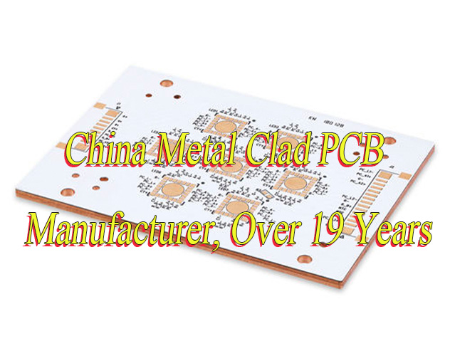
China stands as the global hub for PCB manufacturing, accounting for over 56% of the world’s total output and leading innovations in high-layer boards, HDI technology, and automotive electronics PCBs. For businesses seeking reliable partners, understanding the China top 10 PCB manufacturers is critical to unlocking quality, efficiency, and technical expertise. These leading China PCB manufacturing company entities dominate key segments from AI server PCB China to new energy vehicles, with capabilities ranging from China PCB prototyping service to mass production. Whether you’re sourcing for consumer electronics or industrial control systems, the China top 10 PCB manufacturers represent the gold standard, backed by advanced equipment and global supply chain integration.
Top 10 PCB Manufacturers in China
| Company Name | Process Capabilities | Core Advantages | Address |
|---|---|---|---|
| Huadian Co., Ltd. (002463.SZ) | 64-layer through-hole boards, HDI boards; drilling precision ±15μm | Global leader in AI server PCB China & automotive PCB; 800G switch PCB market share leader | Kunshan, Jiangsu Province |
| Shengyi Electronics (688183.SH) | High-precision PCBs, high-frequency materials (self-sufficiency >80%) | Top 2 in AI server PCB China market share; industry-leading growth | Dongguan, Guangdong Province |
| Shennan Circuit (002916.SZ) | 5G base station RF PCBs, ABF carrier boards | No.1 domestic market share in communication PCB; turnkey solutions | Wuxi, Jiangsu & Shenzhen, Guangdong |
| Shenghong Technology (300476.SZ) | 70-layer high-layer PCB manufacturers China, 8-layer HDI | Exclusive Tesla Cybertruck PCB supplier; IATF 16949 certified | Huizhou, Guangdong Province |
| Guanghe Technology (001389.SZ) | Data center PCBs, AI-specific PCBs | 74% overseas revenue; top 2 net profit margin in A-share PCB | Dongguan, Guangdong & Thailand |
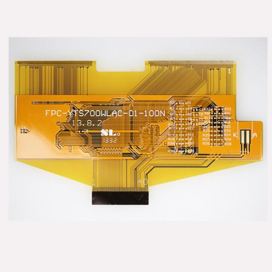
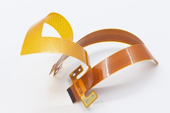
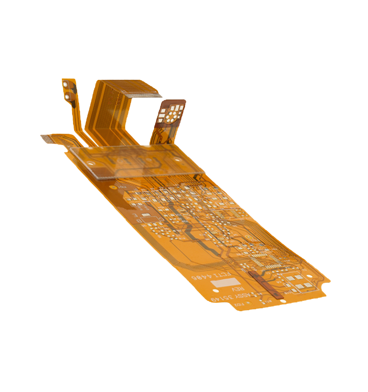
| Dongshan Precision (002384.SZ) | FPC flexible boards, automotive PCBs | Apple’s 2nd largest FPC supplier; Tesla core partner | Changzhou, Jiangsu Province |
| Pengding Holdings (002938.SZ) | FPC (28% global share), SLP carrier boards | 95%+ mass production yield; Apple’s top FPC supplier | Shenzhen, Guangdong Province |
| Jingwang Electronics | Rigid boards, FPC, 5G high-frequency PCBs | 7 global production bases; one-stop procurement | Dongguan, Guangdong & Jiangxi |
| JLCPCB (Jialichuang) | 32-layer prototyping, 0.15mm aperture | 48-hour China PCB prototyping service; EDA to SMT turnkey solutions | Shenzhen, Guangdong Province |
| Liefeng PCB | Military-grade 12+ layer boards, 0.0762mm line width | 24-hour prototyping; 99.9% on-time delivery | Shenzhen, Guangdong Province |
How to Choose a China PCB Manufacturing Company
Selecting the right partner requires aligning needs with strengths. For AI server PCB China projects, prioritize firms like Shengyi Electronics with high-frequency material capabilities. For complex designs, choose high-layer PCB manufacturers China such as Shenghong Technology (70-layer capacity). For rapid iterations, verify China PCB prototyping service lead times (e.g., JLCPCB’s 48-hour delivery). Always check certifications: IATF 16949 for automotive, ISO 13485 for medical.
Core Pain Points of China PCB Manufacturing Company Entities
- Raw material cost pressure (copper, CCL) squeezing margins for high-layer PCB manufacturers China
- Price wars in mid-low end segments, impacting profitability of small China PCB manufacturing company teams
- Skilled technician shortage for advanced HDI PCB suppliers China processes (laser drilling, resin)
- Environmental compliance costs for wastewater treatment and emission reduction
- Supply chain disruptions delaying AI server PCB China component procurement
- Rapid tech (800G PCB, automotive high-speed boards) requiring frequent equipment upgrades
- Quality control challenges for high-layer PCB manufacturers China (±15μm drilling tolerance)
- Rising labor costs in coastal hubs pushing relocation to inland regions
How to Evaluate Production Capacity of China PCB Manufacturing Company
- Equipment Scale: Number of production lines and advanced tools (CNC drilling, automatic exposure) for high-layer PCB manufacturers China
- Output Metrics: Daily SMT placement capacity or monthly AI server PCB China production volume
- Process Maturity: Max layer count (e.g., 70-layer), minimum line width, and HDI for HDI PCB suppliers China
- Certifications: ISO 9001, IATF 16949, or ISO 13485 with yield data (e.g., 95%+ for Pengding Holdings)
- R&D Investment: Annual spending on AI server PCB China or high-frequency material innovation
- Workforce Strength: Size of engineering teams trained in advanced PCB processes
- Fulfillment Rate: On-time delivery stats for China PCB prototyping service and mass production
- Expansion Plans: New plants (e.g., Huadian’s 4.3B yuan project) ensuring long-term supply
How to Evaluate Lead Time of China PCB Manufacturing Company
- Production Scheduling: ERP-integrated systems optimizing China PCB prototyping service sequencing
- Cycle Differentiation: Standard lead times (24-hour prototyping, 7-14 days mass production) and expedited options
- Supply Chain Proximity: Local sourcing of CCL and solder paste to avoid delays
- Line Utilization: 70-85% capacity rate to prevent overbooking for AI server PCB China orders
- Quality Testing: Automated AOI/X-ray inspection reducing rework delays
- Logistics Partnerships: DHL/FedEx collaborations for domestic/international delivery
- Emergency Plans: Backup production lines for high-layer PCB manufacturers China equipment failures
- Real-Time Tracking: Order monitoring systems and dedicated account managers
- Historical Data: 99.9% on-time rate (e.g., Liefeng PCB) for similar order sizes
- Contract Terms: Late delivery penalties ensuring accountability
Common Problems & Solutions for China PCB Manufacturing Company (FAQ)
Problem: Signal loss in AI server PCB China and 5G applications.
Solution: Adopt self-produced high-frequency materials (Shengyi’s 80%+ self-sufficiency) and optimize layouts via EDA design.
Problem: Delays from raw material shortages for HDI PCB suppliers China.
Solution: Partner with multiple CCL suppliers and maintain safety stock for critical components.
Problem: Low yield in high-layer PCB manufacturers China production.
Solution: Invest in laser drilling, 100% AOI inspection, and precision control training (Pengding’s 95%+ yield model).
Problem: High cost of small-batch China PCB prototyping service.
Solution: Use intelligent panelization (JLCPCB’s optimization) to reduce waste and offer flexible pricing.
Problem: Inconsistent quality across China PCB manufacturing company batches.
Solution: Implement IoT-enabled real-time monitoring and standardized shift procedures.
Core Summary
Understanding the China top 10 PCB manufacturers provides curated high-quality partners, and leveraging selection criteria, capacity evaluation, and problem-solving ensures successful collaboration with the China top 10 PCB manufacturers—whether sourcing AI server PCB China, high-layer PCB manufacturers China, or China PCB prototyping service solutions.