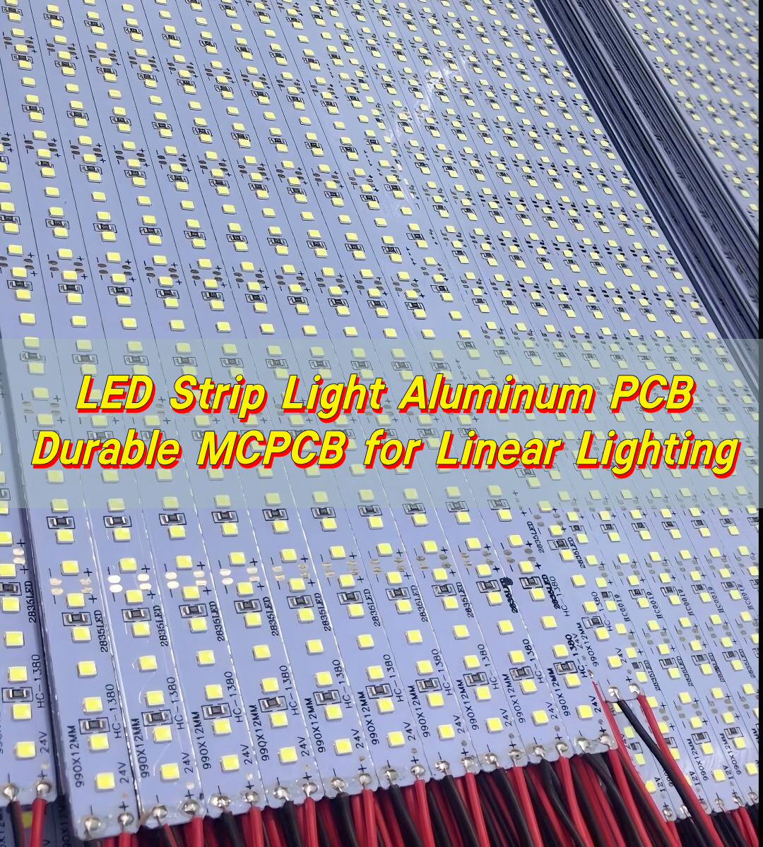
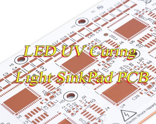
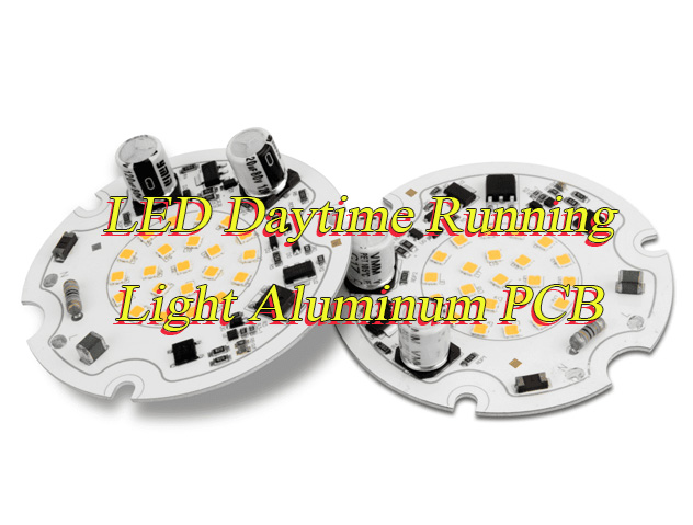
Why should you choose LED daytime running light aluminum PCB to avoid common DRL failures? If your LED daytime running lights suffer from overheating, brightness fade, or short lifespan, the right LED daytime running light aluminum PCB is the solution you need. For reliable, high-performance LED DRL aluminum PCBs, choose EBest, we guarantee consistent quality, fast delivery, stable supply chain, and professional service to meet all your DRL production needs.
This blog breaks down everything you need to know about LED daytime running light aluminum PCBs, from solving overheating to ensuring durability, helping you make informed decisions and avoid costly mistakes.
Why Do LED DRL Aluminum PCBs Solve Overheating Issues?
LED DRL aluminum PCBs solve overheating by leveraging aluminum’s natural thermal conductivity and optimized design, addressing the root cause of heat buildup in long-running DRLs. Unlike traditional PCBs that trap heat, aluminum PCBs are engineered to efficiently move heat away from critical components, ensuring DRLs operate safely and consistently even during extended use.
- Superior Thermal Conductivity of Aluminum Core: Aluminum is a naturally excellent thermal conductor, with a thermal conductivity range of 170-220 W/mK. This is drastically higher than traditional FR4 PCBs, which only offer 0.3 W/mK. This difference means heat generated by LED chips transfers quickly through the aluminum core, rather than accumulating on the board.
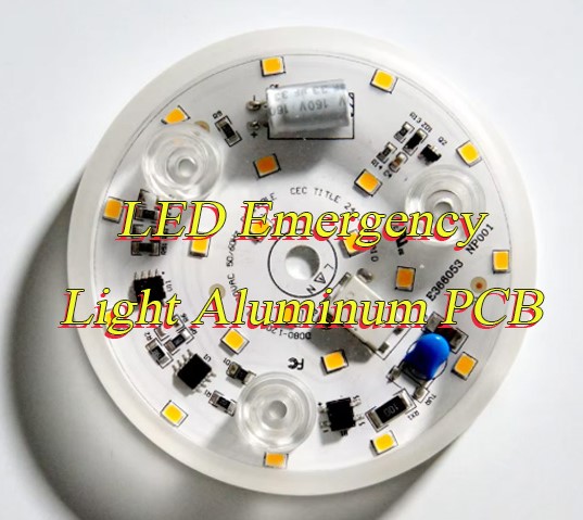
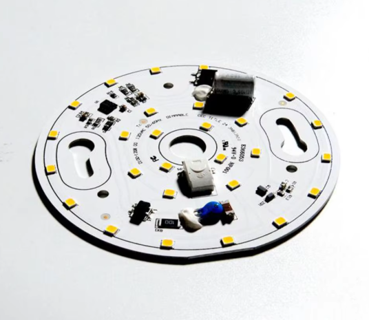
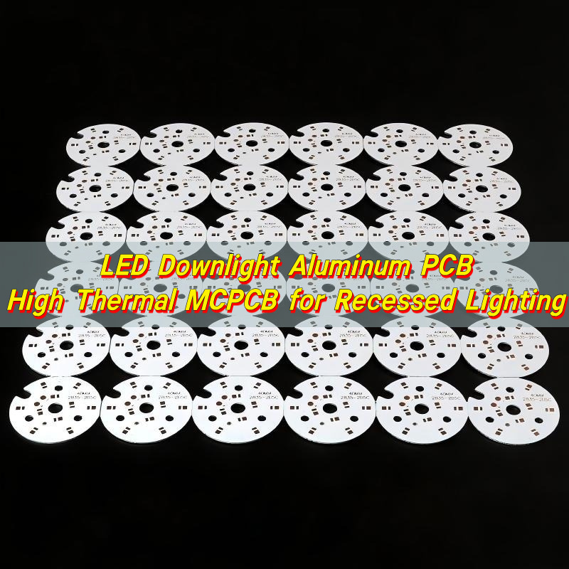
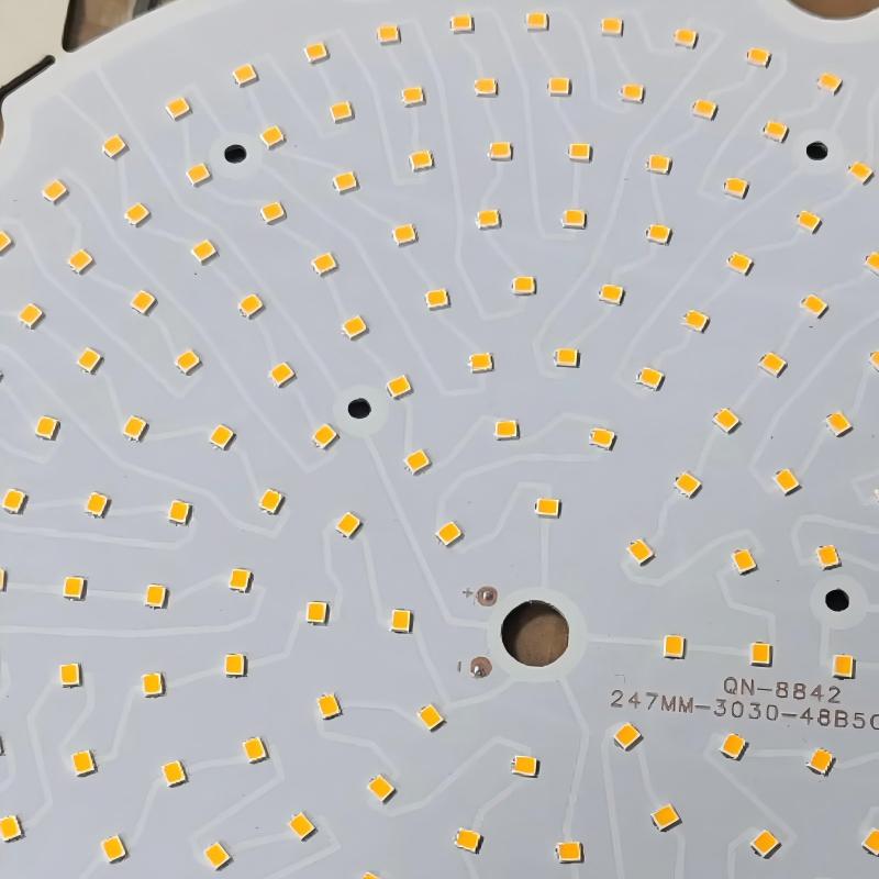
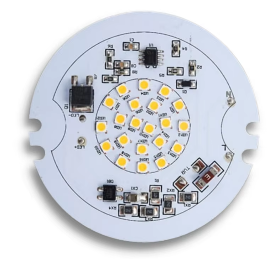
- Optimized Three-Layer Structure: LED DRL aluminum PCBs feature a three-layer design, circuit layer, thermal insulation layer, and aluminum base that works in tandem to direct heat away from LEDs. The circuit layer holds the LED chips, the thermal insulation layer prevents electrical short circuits while enabling heat transfer, and the aluminum base acts as a heat sink to dissipate heat into the surrounding air.
- Uniform Heat Distribution to Prevent Hotspots: Overheating in DRLs is often caused by hotspots, small areas where heat concentrates. Aluminum’s ability to distribute heat evenly across the entire PCB surface eliminates these hotspots. This uniform heat spread ensures no single component is exposed to excessive temperatures, reducing the risk of damage or performance loss.
- Compatibility with High-Power LED DRLs: Modern LED DRLs often use high-power chips to produce brighter light, which generates more heat. Aluminum PCBs can handle this increased heat load without compromising performance, making them ideal for high-power DRL applications where traditional PCBs would fail due to overheating.
- Adaptability to Automotive Operating Conditions: DRLs operate in harsh automotive environments, including high under-hood temperatures and direct sunlight. Aluminum PCBs are designed to withstand these conditions, maintaining their thermal performance even when exposed to external heat sources, further preventing overheating.
What Makes LED DRL Aluminum PCBs More Durable Than Regular PCBs?
LED daytime running light aluminum PCB are more durable than regular PCBs due to superior material strength, thermal stability, and resistance to harsh automotive conditions.
| Performance Feature | LED DRL Aluminum PCB | Regular FR4 PCB |
| Thermal Stability | Withstands -40°C to 125°C; maintains performance after 1,000 extreme temperature cycles | Withstands -20°C to 85°C; prone to warping and delamination at high temperatures |
| Mechanical Strength | High tensile strength (390 MPa); resistant to automotive vibration and impact | Brittle (220 MPa); easily cracks or fractures under vibration |
| Longevity (Continuous Use) | 50,000+ hours; MTBF >100,000 hours | 20,000-30,000 hours; rapid degradation in DRL applications |
| Moisture & Corrosion Resistance | Low water absorption rate; resists salt spray and humidity; suitable for harsh automotive environments | Prone to moisture absorption; easily corroded in humid or salty conditions |
| Layer Adhesion | Strong layer bonding; maintains integrity after extreme temperature cycles | Poor adhesion; layers separate easily under thermal stress |
How Can LED DRL Aluminum PCBs Prevent Brightness Fade?
LED daytime running light aluminum PCB prevent brightness fade by addressing the core causes of LED performance degradation, including excess heat, thermal stress, and uneven current distribution, all while maintaining consistent operation over time.
- Maintain Optimal LED Operating Temperatures: LED chips degrade quickly when overheated, as 60%-70% of their energy converts to heat during operation. Aluminum PCBs keep LED chips within the 50-60°C optimal range, preventing heat-induced damage that causes gradual brightness fade.
- Minimize Thermal Stress with CTE Matching: The thermal expansion coefficient (CTE) of aluminum PCBs closely matches that of LED chips. This reduces stress from temperature changes, avoiding physical damage to LED connections and ensuring consistent brightness output.
- Ensure Uniform Heat and Current Distribution: Aluminum’s excellent thermal conductivity spreads heat evenly across the PCB, eliminating hotspots. This uniform heat distribution also ensures consistent current flow to all LEDs, preventing uneven brightness or premature fade in individual chips.
- Reduce Thermal Resistance for Stable Performance: Aluminum PCBs have low thermal resistance, allowing heat to escape quickly instead of accumulating around LED chips. Lower thermal resistance keeps LEDs operating efficiently, preserving their brightness over long-term use.
- Protect LEDs from Voltage Fluctuations: The stable thermal performance of aluminum PCBs helps regulate voltage flow to LEDs. This prevents voltage spikes or drops that can damage LED chips and cause erratic brightness or fade.
Why Are Aluminum PCBs Better for Compact LED DRL Designs?
Aluminum PCBs stand out for compact LED DRL designs because they seamlessly combine high thermal efficiency with space-saving features, eliminating the need for bulky accessories and adapting to tight automotive enclosures.
- Slim, Space-Saving Profile: LED DRL aluminum PCBs can be as thin as 0.8mm, with the most common thickness range (1.0-1.6mm) perfectly fitting tight DRL enclosures. This slim design avoids taking up excess space while maintaining full thermal performance.
- Integrated Heat Dissipation Eliminates Bulky Heat Sinks: Unlike regular PCBs that require separate, bulky heat sinks to manage heat, aluminum PCBs use their aluminum base as a built-in heat sink. This removes the need for extra components, reducing overall DRL size and weight significantly.
- Lightweight Construction: Aluminum is lighter than traditional PCB materials, making LED DRL aluminum PCBs ideal for compact designs where weight reduction is critical (e.g., electric vehicles). They reduce DRL weight without compromising durability or performance.
- Flexible Shaping for Unique Enclosures: LED DRL aluminum PCBs can be formed into 3D shapes and curved profiles, adapting to the sleek, unique designs of modern compact DRLs. This flexibility eliminates the need to modify enclosures to fit rigid PCBs.
- High Thermal Efficiency in Small Footprints: Even in compact sizes, aluminum PCBs maintain excellent thermal conductivity (170-220 W/mK), ensuring heat dissipates quickly. This prevents overheating in small DRL enclosures where heat buildup is a common issue.
- Compatibility with High-Density LED Layouts: Compact DRLs often use high-density LED layouts to maximize brightness in a small space. Aluminum PCBs support tight component spacing without overheating, allowing for brighter, more efficient DRLs in minimal space.
How to Choose Cost-Effective LED Daytime Running Light Aluminum PCB in Bulk?
Below is a selection guide to cost-effective LED daytime running light aluminum PCB:
- Prioritize aluminum core quality: Optimize for 5052 or 6061 aluminum alloy, which offer ideal thermal conductivity and mechanical strength for LED DRL applications.
- Select high-quality insulation layers: Choose epoxy or polyimide insulation to ensure electrical safety and efficient heat transfer without adding unnecessary cost.
- Ensure consistent copper thickness: Stick to 35-70um copper layers, which balance conductivity, cost, and compatibility with LED DRL components.
- Check dimension accuracy: Require ±0.15mm dimension precision to avoid fitting issues and reduce rework costs during bulk assembly.
- Evaluate supplier’s supply chain stability: Partner with suppliers who can guarantee steady bulk delivery to prevent production delays and extra costs.
- Request pre-bulk samples: Test a small batch first to verify quality, thermal performance, and compatibility before placing large orders.
- Avoid over-specification: Choose thermal conductivity (1-3 W/mK) based on your DRL power needs, not unnecessary high specs that increase costs.
- Look for consistent manufacturing standards: Ensure suppliers follow strict quality control to avoid batch-to-batch inconsistencies that cause waste.
- Consider panel size efficiency: Optimize for standard 480x580mm panels for bulk production to minimize material waste and lower per-unit costs.
What Thermal Conductivity Do LED DRL Aluminum PCBs Need?
The required thermal conductivity for LED daytime running light aluminum PCB depends on the power of your LED DRLs, as higher power generates more heat that requires efficient dissipation. Most automotive LED DRLs require a thermal conductivity range of 1-3 W/mK for optimal results, with specific values tailored to power output.
| LED DRL Power Range | Recommended Thermal Conductivity (W/mK) | Considerations |
| Low-Power (≤3W) | 1-1.5 | Sufficient for compact, budget-friendly DRLs; balances heat dissipation and cost-efficiency without over-specification. |
| Medium-Power (3-10W) | 1.5-2.5 | Most common for modern automotive DRLs; prevents overheating and hotspots during long-term operation, ensuring stable performance. |
| High-Power (>10W) | 2.5-3 or higher | Ideal for premium, high-visibility DRLs; pairs with advanced thermal insulation layers to handle significant heat output effectively. |
How Do LED Daytime Running Light Aluminum PCB Reduce Energy Consumption?
LED daytime running light aluminum PCB reduce energy consumption through optimized thermal management and material efficiency. Here’s how:
- Enhanced Heat Dissipation: Aluminum’s high thermal conductivity (up to 2.0 W/m·K) minimizes heat buildup, allowing LEDs to operate at lower temperatures with reduced power draw.
- Thinner Substrate Design: Thinner aluminum layers improve heat transfer efficiency, cutting cooling system energy use by up to 30% compared to FR-4 PCBs.
- Reduced Resistance Losses: Aluminum’s low electrical resistance decreases power loss in traces, boosting overall circuit efficiency.
- Compact Circuit Layout: Streamlined layouts minimize copper trace lengths, lowering parasitic capacitance and energy waste.
- Long-Term Stability: Durable aluminum resists thermal cycling stress, maintaining consistent performance and avoiding energy spikes from degraded components.
Why Do LED DRLs Fail Without High-Quality Aluminum PCBs?
High-quality LED DRL aluminum PCBs are the foundation of reliable DRL performance. Without them, DRLs face premature failure, as they lack the thermal management and material stability needed for automotive use.
Overheating is the top cause of DRL failure without quality aluminum PCBs. LED chips generate significant heat during operation, and low-quality PCBs trap this heat instead of dissipating it.
Trapped heat damages LED chips and solder joints over time, leading to sudden DRL shutdowns or dimmed performance that renders the lights ineffective for safety.
Low-quality PCB materials degrade quickly in harsh automotive conditions. Extreme temperature changes cause warping or cracking, breaking electrical connections critical to DRL function.
Poor insulation layers in low-grade PCBs allow moisture to seep in, especially in humid or coastal environments. This leads to short circuits and corrosion of components.
Without the thermal stability of high-quality aluminum PCBs, LED chips degrade faster, reducing brightness and lifespan, creating costly replacements and maintenance issues.
Even minor material inconsistencies in low-quality PCBs cause inconsistent performance, leading to some DRLs failing earlier than others in a batch.
LED DRLs fail without high-quality aluminum PCBs because poor heat dissipation, unstable materials, and thermal stress lead to component damage and performance degradation.
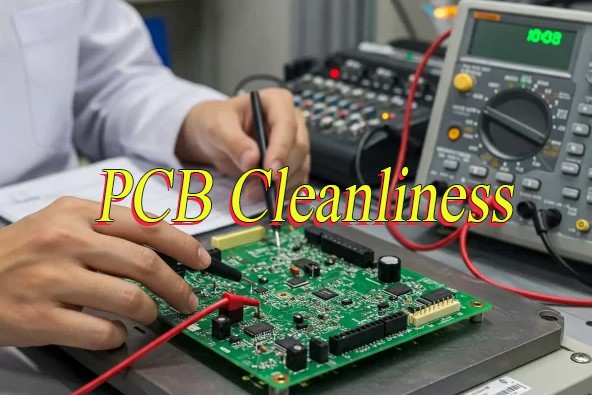
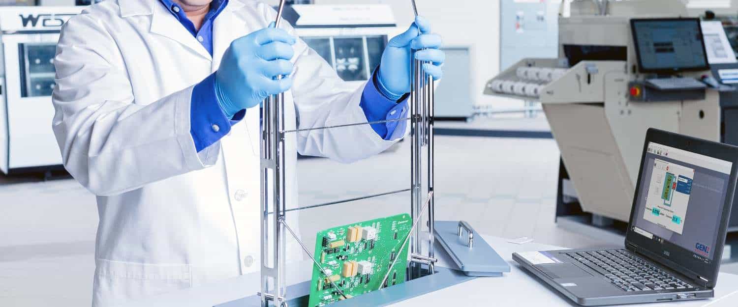
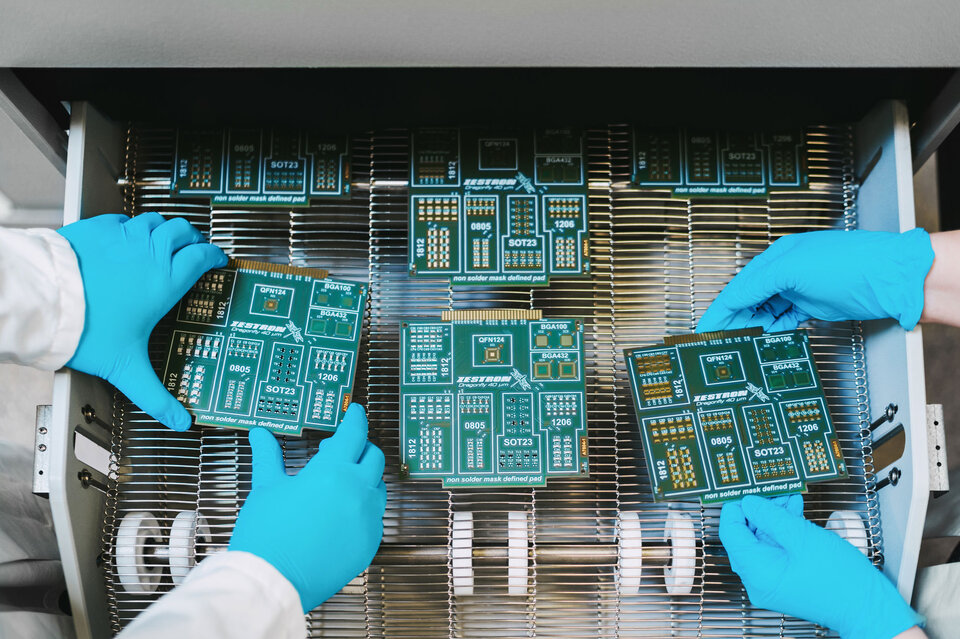
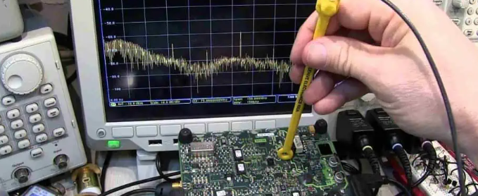
How to Ensure Stable Quality of LED Daytime Running Light Aluminum PCB?
Below are methods to ensure stable quality of LED daytime running light aluminum PCB:
- Material Selection: Use high-purity aluminum substrates (e.g., 1050/1060 series) for optimal thermal conductivity (≥1.5W/m·K) and mechanical robustness, ensuring consistent performance under thermal stress.
- Precision Manufacturing: Implement tight process controls for etching, lamination, and drilling to maintain dimensional accuracy (±0.1mm tolerance) and prevent defects like delamination or warping.
- Surface Treatment: Apply uniform solder mask and electroplated finishes (e.g., ENIG) to enhance solderability and corrosion resistance, reducing oxidation risks during assembly.
- Thermal Management Validation: Conduct thermal cycling tests (e.g., -40°C to 125°C) and IR thermal imaging to verify heat dissipation efficiency and identify hotspots before mass production.
- Electrical Performance Testing: Perform impedance, insulation resistance, and dielectric withstanding voltage tests per IPC-TM-650 standards to ensure signal integrity and safety compliance.
- Process Monitoring & Feedback: Integrate real-time SPC (Statistical Process Control) for critical parameters (e.g., thermal conductivity, layer thickness) to detect deviations early and enable corrective actions.
- Supplier Quality Collaboration: Partner with certified suppliers for raw materials and components, enforcing strict incoming inspection (e.g., AQL 0.65) to prevent substandard inputs.
- Environmental Adaptability Checks: Test under humidity (85% RH), vibration, and shock conditions to confirm durability for automotive-grade applications (e.g., IP67/IP69K compliance).
- Documentation & Traceability: Maintain detailed batch records (e.g., material certs, process logs) and implement traceability systems (e.g., QR codes) for quality audits and recall readiness.
FAQ About LED DRL Aluminum PCBs
Q1: Can LED DRL aluminum PCBs work in extreme cold or hot climates?
A1: Yes, LED DRL aluminum PCBs are designed to withstand extreme automotive climates. They operate reliably from -40°C to 125°C, making them suitable for all regions, from cold northern areas to hot deserts. Their thermal stability prevents warping or performance loss in extreme temperatures.
Q2: How long do LED DRL aluminum PCBs last in continuous use?
A2: LED DRL aluminum PCBs last 50,000+ hours of continuous use, which is more than double the lifespan of regular FR4 PCBs. This longevity reduces replacement frequency and maintenance costs, making them ideal for long-term DRL applications.
Q3: Do LED DRL aluminum PCBs require special installation?
A3: No, LED DRL aluminum PCBs do not require special installation. They use the same mounting methods as regular PCBs, including soldering and screw mounting. Their slim profile and lightweight design make installation quick and straightforward, fitting into existing DRL assemblies.
Q4: Can I get custom-sized LED DRL aluminum PCBs for my unique DRL design?
A4: Yes, custom-sized LED DRL aluminum PCBs are available. Reliable suppliers like EBest offer custom cutting, shaping, and thickness options to fit unique DRL designs, including 3D formed shapes for curved or compact enclosures, which is ideal for adapting to the complex structural requirements of automotive lighting.
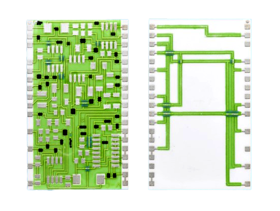
Q5: How do LED DRL aluminum PCBs compare to ceramic PCBs in terms of performance?
A5: LED DRL aluminum PCBs offer better value and practicality than ceramic PCBs for most automotive applications. Ceramic PCBs have higher thermal conductivity but are more expensive and brittle. Aluminum PCBs provide sufficient thermal performance (1-3 W/mK) at a lower cost, with better mechanical strength for automotive use.