

A UFL Connector PCB is a printed circuit board that integrates an ultra-miniature U.FL RF connector to provide a compact, low-loss interface between an onboard RF module and its antenna. In the world of ever-shrinking wireless devices, from IoT sensors to compact wearables, reliable radio frequency (RF) connectivity is paramount. Achieving this in a minimal footprint requires specialized components, and the UFL connector PCB is a critical enabler. This article explores everything you need to know about integrating these tiny yet powerful connectors into your printed circuit board (PCB) designs for optimal wireless performance.
Are you constantly battling signal integrity issues, manufacturing headaches, and costly delays when integrating miniature UFL connectors into your compact RF designs? Common Pain Points in UFL Connector PCB Integration:
- Signal Loss and Mismatch: Even a minor imperfection in the PCB layout or manufacturing can cause impedance discontinuities, leading to poor VSWR, signal reflection, and drastically reduced wireless range and data throughput.
- Fragility and Mechanical Failure: The connectors themselves are delicate. Improper handling during assembly or end-use can lead to broken clips, cracked housings, or the center pin detaching from the cable, rendering the RF path useless.
- Complex and Inconsistent Soldering: The miniature size of SMT UFL connectors makes manual soldering highly challenging, often resulting in cold solder joints, solder bridges, or thermal damage to the plastic housing, causing failures that are difficult to diagnose.
- Incorrect Footprint Design: Using a generic land pattern from a CAD library without verifying the specific connector’s datasheet can result in misalignment during pick-and-place, poor soldering yield, and compromised mechanical strength.
- Limited Mating Cycles and Wear: The UFL connector is rated for a limited number of connections and disconnections (typically 20-30 cycles). Frequent testing during prototyping can quickly wear out the connector, leading to intermittent contact and unreliable performance in the final product.
Addressing these challenges requires a partnership with a manufacturer that possesses deep expertise in RF design and precision manufacturing. By moving from a standard PCB fabricator to a specialized RF partner, these pain points can be systematically eliminated.
- Guaranteed Impedance Control: We employ advanced impedance modeling and use controlled-Dk materials to ensure the microstrip line feeding the connector maintains a consistent 50-ohm impedance, minimizing losses and ensuring optimal RF power transfer from your module to the antenna.
- Robust DFM Analysis and Support: Our engineering team provides a thorough Design for Manufacturability (DFM) review, specifically analyzing your UFL connector footprint and layout to recommend optimizations that enhance mechanical strength and prevent common assembly defects.
- High-Precision SMT Assembly: Utilizing automated optical inspection (AOI) and precision pick-and-place systems, we ensure perfect alignment and consistent, high-quality solder joints for UFL connectors, eliminating the variability and defects associated with manual soldering.
- Verified PCB Land Patterns: We maintain an extensive library of certified component footprints and work with you to verify that the land pattern for your chosen UFL connector is optimized for both soldering reliability and RF performance.
- Prototyping and Testing Support: We provide dedicated test coupons and prototype assemblies to allow you to validate your design without wearing out the connectors on your main production boards, extending their lifespan for the final product.
BEST Technology stands as a trusted PCB and PCBA partner for engineers demanding uncompromising quality and reliability in high-frequency PCB and PCBA solutions. We specialize in the precise manufacturing and assembly of complex designs, with deep expertise in impedance control and the micro-assembly of miniature components like UFL connectors. By leveraging state-of-the-art equipment and rigorous quality processes, we ensure your advanced wireless products perform flawlessly from prototype to high-volume production. A warm welcome to contact us to discuss your project requirements by sales@bestpcbs.com.
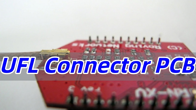
What Is a UFL Connector PCB?
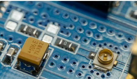
A UFL Connector PCB is a printed circuit board that has been designed to integrate a specific type of miniature RF connector: the U.FL connector.
- Official Definition & Origin
The U.FL connector is a miniature, coaxial radio frequency connector series officially developed by the Hirose Electric Group. It is formally known as the “Hirose U.FL Series.” - Primary Function
Its core purpose is to establish a secure yet detachable connection between a radio frequency (RF) module on the PCB and an antenna. This allows for flexible antenna placement while keeping the main board compact. - Key Physical Characteristics
The connector is characterized by its extremely small size and light weight (often weighing just a few tenths of a gram). This makes it the ideal solution for space-constrained applications where larger standard connectors (like SMA) are not feasible. - Design Intention & Usage Note
It is crucial to note that the U.FL connector is engineered for a limited number of mating cycles (typically between 20 to 30). This design specifies that it is intended for a semi-permanent connection, which is established once during the manufacturing or assembly process and not for frequent disconnection in daily use.
How Does a UFL PCB Connector Enable RF Signals on Compact Devices?
The UFL PCB connector serves as a critical bridge for RF signals in space-limited electronics. Its functionality can be broken down into the following key aspects:
- Design Flexibility
This setup decouples the antenna’s location from the main PCB. Designers can position the main board optimally for the device’s electronics and use a short cable to place the antenna in an ideal location for the best possible reception and transmission performance.
- Signal Path Establishment
The RF signal originates from the transceiver chip on the PCB. It is carefully routed via a controlled-impedance microstrip transmission line—a precise pathway etched onto the board—which terminates directly at the solder pads of the UFL connector.
- Shielded Transmission
The UFL connector itself is a miniature coaxial system. It provides a fully shielded path, ensuring the high-frequency signal is transmitted from the board to the antenna cable with minimal loss and protection against electromagnetic interference (EMI).
What Are the Differences Among UFL U.FL IPX IPEX PCB Connector Standards?
This is a common source of confusion. Essentially, UFL, U.FL, IPX, and IPEX are often used interchangeably, but there are nuances:
- U.FL (Hirose): This is the original brand name from Hirose. It is the de facto standard.
- IPEX/IPX (I-PEX): I-PEX is a direct competitor to Hirose and manufactures a visually identical connector series. The terms are used generically, much like “Kleenex” for tissues.
- Compatibility: In practice, UFL U.FL IPX IPEX PCB connector products are often mechanically compatible and can be mated with each other. However, for critical applications, it’s best to specify the exact manufacturer and series to ensure electrical and mechanical specifications are perfectly matched.
How to Determine the Right UFL Connector PCB Size for Your RF Module?
Selecting the correct UFL connector PCB size is crucial. The “size” refers to the connector’s footprint and height. Most standard UFL connectors have a very similar PCB footprint, but variations exist in height and cable exit angle (vertical, right-angle). To determine the right size:
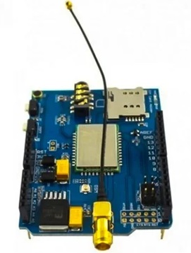
- Check Your RF Module: Many pre-certified RF modules (e.g., Wi-Fi, Bluetooth) come with a recommended UFL connector part number.
- Review Mechanical Constraints: Measure the available vertical clearance (Z-height) on your PCB. A right-angle connector is common for saving vertical space.
- Consult Datasheets: Always refer to the manufacturer’s datasheet for the exact land pattern (footprint) and recommended PCB layout to ensure proper impedance matching.
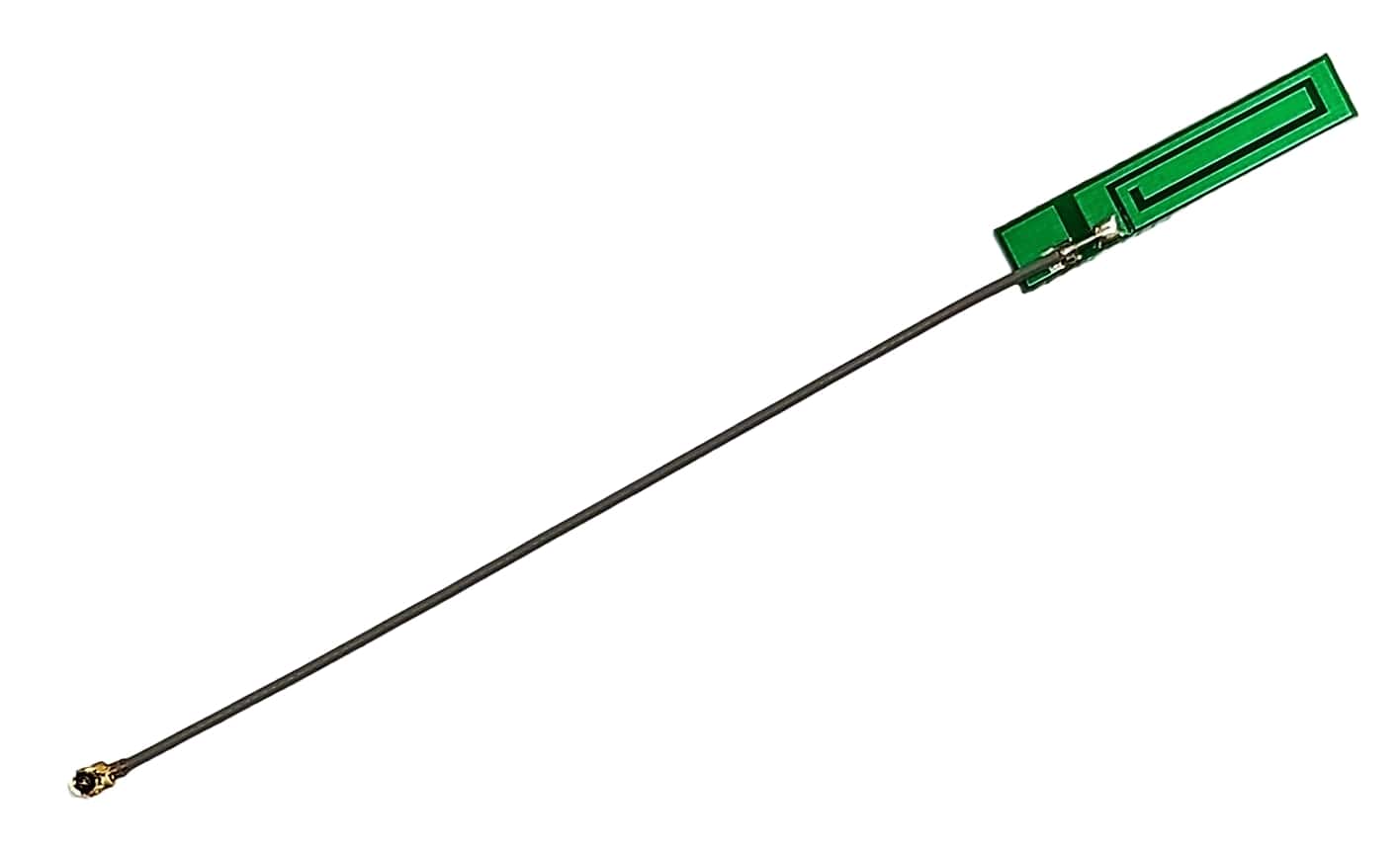
When Should You Use a UFL Connector PCB Adapter to Extend Antenna Routing?
A UFL connector PCB adapter (or pigtail) is a short cable with a UFL connector on one end and another connector (like SMA) on the other. You should use one in these scenarios:
- Prototyping and Testing: Easily connect your PCB to a large, external antenna or test equipment.
- Final Assembly: When the optimal antenna location is far from the main PCB.
- Connecting to an External Antenna: To interface with a chassis-mounted antenna connector, a UFL connector to SMA pigtail is the standard method.
How Does a UFL SMT Antenna Connector Improve Wireless Performance in Small PCBs?
The UFL SMT (Surface-Mount Technology) antenna connector significantly enhances the wireless performance of compact PCB designs through several key advantages inherent to its SMT nature:
- Precision and Manufacturing Consistency
As an SMT component, it is ideal for high-speed, automated PCB assembly. This process ensures exceptionally high placement precision and consistency, which is critical for radio frequency (RF) circuits. - Stable RF Performance
Any variation in the connector’s placement or soldering can detune the sensitive RF matching circuit, leading to significant signal loss. The manufacturing consistency of SMT mounting eliminates this variability, guaranteeing the RF performance designed into the board is reliably achieved in every unit. - Mechanical and Electrical Reliability
The SMT design creates a low-profile connection that is mechanically robust against vibration and stress. Simultaneously, it provides an electrically stable path that maintains a consistent 50-ohm impedance from the board to the connector, minimizing signal reflections and ensuring optimal power transfer.
In summary, the UFL SMT connector improves wireless performance by enabling manufacturing precision that translates directly into electrical stability, ensuring reliable and consistent signal integrity in space-constrained applications.
What Is the Correct UFL Connector Pinout for Reliable RF Matching?
The UFL connector pinout is straightforward. A standard UFL connector has three terminals:
- Center Pin (Signal): This solders to the RF signal pad on the PCB, which is the end of the 50-ohm microstrip line.
- Two Outer Ground Pads: These are soldered to the ground plane on the PCB. A proper UFL connector PCB layout will have these pads connected to the ground plane with multiple vias placed immediately adjacent to the pads. This provides an excellent low-inductance ground return path, which is critical for RF matching and shielding.
Why Does UFL Connector PCB Performance Depend on High-Quality RF Board Manufacturing?
UFL connector PCB design and manufacturing quality are non-negotiable. RF signals are extremely sensitive to the characteristics of the PCB material and the physical geometry of the traces. High-quality RF PCB manufacturing ensures:
- Consistent Dielectric Constant: Using materials like FR-4 with controlled RF characteristics or specialized laminates like Rogers.
- Precise Impedance Control: The microstrip line leading to the connector must be exactly calculated and fabricated to be 50 ohms.
- Proper Grounding: A continuous ground plane is essential. The manufacturing process must ensure there are no voids or inconsistencies.
Poor manufacturing can lead to impedance mismatches, resulting in signal reflections, high VSWR, and drastically reduced range and data throughput.
Why Partner With EBest Circuit (Best Technology) for Complex UFL Connector PCB and PCBA Builds?
Integrating a UFL connector PCB mount successfully requires expertise in both RF design (PCB layout) and assembly (PCBA). Partnering with a specialist like EBest Circuit (Best Technology) ensures:
- Impedance Control Expertise: We accurately model and control the impedance of your RF traces.
- DFM for RF Components: We provide Design for Manufacturability (DFM) feedback to optimize your UFL connector PCB layout for reliable, high-yield assembly.
- Precision Assembly: Our SMT lines can accurately place the tiny UFL SMT antenna connector, ensuring perfect alignment and soldering for optimal performance.
- Comprehensive Support: From material selection and stack-up design to final assembly and testing, we manage the entire process to ensure your wireless design performs as intended.
In a nutshell, a well-designed and well-manufactured UFL Connector PCB is essential for stable RF performance in today’s compact wireless devices. Because UFL connectors demand precise impedance control, accurate land patterns, clean grounding, and high-quality SMT assembly, partnering with an experienced manufacturer is key to avoiding signal loss, mismatch, and reliability issues. With advanced RF PCB fabrication, strict process control, and precision PCBA capabilities in both China and Vietnam, EBest Circuit (Best Technology) ensures your UFL-based designs perform consistently from prototype to mass production. For professional support with your next RF PCB or PCBA project, you are welcome to reach us at sales@bestpcbs.com.
FAQs about UFL Connector PCB
What is the difference between W FL and U FL connectors?
- The W.FL is another miniature Hirose connector series, slightly larger and more robust than the U.FL, rated for more mating cycles (up to 100). The U.FL is the smallest, while the W.FL offers a better trade-off between size and durability.
Is U.FL the same as Ipex?
- Not exactly. U.FL is a specific product series from Hirose, while IPEX (or IPX) is from I-PEX. They are competitors whose products are mechanically and electrically similar, often interchangeable, but they are different brands.
What is the difference between MHF4 and UFL connectors?
- The MHF4 (also known as HSPM or Hirose Micro Miniature Coaxial Connector) is even smaller than the U.FL connector. It’s designed for extremely compact applications like M.2 cards and is not mechanically compatible with U.FL connectors.
How to solder an UFL connector?
Soldering a UFL connector requires a fine-tip soldering iron, flux, and thin solder.
- Apply a small amount of flux to the PCB pads.
- Pre-tin the center signal pad with a tiny amount of solder.
- Carefully place the connector, ensuring it’s aligned correctly.
- Gently heat the pre-tinned pad to reflow the solder and secure the center pin.
- Solder the two outer ground pads.
- Inspect under a microscope to ensure no solder bridges exist between the signal and ground. Using a hot air rework station with a stencil is the recommended method for production.