

Design and prototyping of single sided printed circuit board is pivotal in electronic Products. This blog aims to provide the basic definition, layer structure, benefits, standardized production processes, and the keys to improving layout efficiency for single sided printed circuit board.
As a technologically advanced OEM supplier, EBest Circuit (Best Technology) delivers the design and prototyping of single sided printed circuit board for global clients. Quality is paramount for gaining our customers’ trust. Our PCB ranges include FR4 PCB, MCPCB, ceramic PCB, and PCBA. We are the original factory providing fast turnaround and high-quality solutions to you. Any single sided printed circuit board projects, just feel free to let us know at sales@bestpcbs.com and we will be happy to provide our best service to you.
What is a Single Sided Printed Circuit Board?
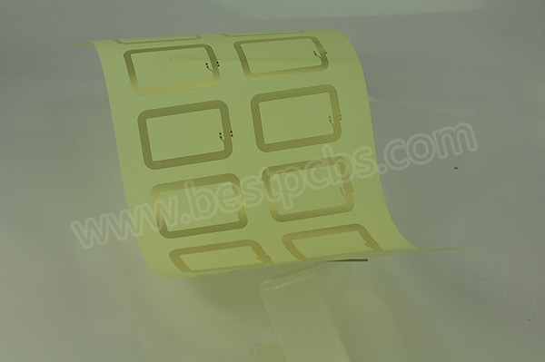
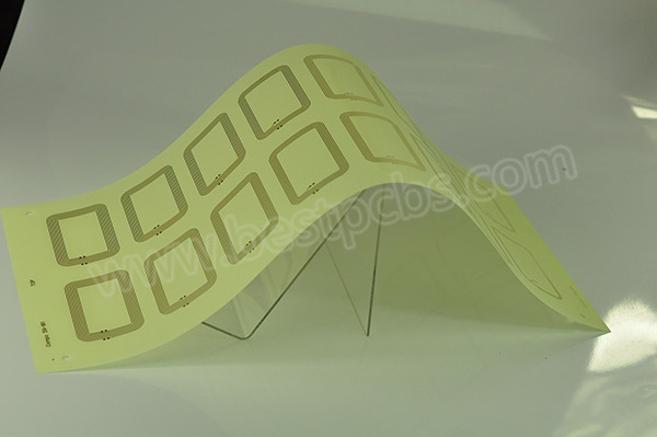
A single sided printed circuit board (single sided PCB) is the most fundamental type of PCB, featuring conductive traces on only one side of an insulating substrate. Components are primarily mounted on the opposite side of the trace layer (or surface-mounted on the same side), with electrical connections established through solder pads. Its core structure includes an insulating substrate (common materials like FR-4, aluminum base, etc.) and a single-sided copper foil layer, which is etched to form specific circuit patterns. Thanks to its “single-layer wiring” design, this PCB ensures basic electrical connectivity while significantly reducing manufacturing complexity and cost, making it the preferred choice for simple electronic systems.
Stackup of Single Sided Printed Circuit Boards
The stackup (layer structure) of single sided PCBs is relatively simple, mainly composed of two basic layers:
- Insulating Substrate Layer: Serves as the circuit carrier, with common materials including FR-4 epoxy glass fiber boards (general-purpose, cost-effective), aluminum substrates (excellent heat dissipation for power circuits), and paper substrates (low-cost, suitable for consumer electronics). Thickness typically ranges from 0.4mm to 3.2mm, selected based on mechanical strength and electrical performance requirements.
- Single-Sided Copper Foil Layer: Covers one side of the substrate, with standard thicknesses of 18μm (0.5oz), 35μm (1oz), and 70μm (2oz). It is etched to form conductive traces for current transmission and signal connection.
This single-layer wiring design limits complex circuit implementation but achieves an efficient balance between cost and performance through reasonable trace routing and component layout.
Core Advantages of Single Sided Printed Circuit Boards
- Low Manufacturing Cost: Eliminates complex processes like multi-layer lamination and via plating, reducing material and processing costs by 30%-50% compared to double-sided/multi-layer boards, ideal for mass production.
- Short Process Cycle: Omits double-sided alignment and inner-layer processing, enabling prototype delivery in as fast as 24 hours to accelerate product iteration.
- Solid Reliability: Single-layer traces eliminate interlayer connection failure risks. After surface treatment (such as HASL, OSP), they meet long-term use requirements in general environments.
- Low Design Threshold: Requires no complex interlayer signal coordination, suitable for entry-level circuit development and convenient for manual soldering and post-maintenance.
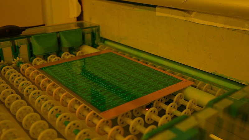
Production Process of Single Sided Printed Circuit Boards
(1) Raw Material Preparation
- Material Cutting: Cut insulating substrates (e.g., FR-4) to design dimensions with a precision of ±0.1mm.
- Copper Foil Preprocessing: Clean the single-sided copper-clad board to remove surface oxidation and ensure optimal etching results.
(2) Circuit Pattern Formation
- Drilling: Use CNC drilling machines to process mounting and positioning holes with a diameter tolerance of ±0.05mm.
- Pattern Transfer: Transfer circuit designs to the copper foil surface via photoresist exposure and development, with minimum line width/spacing controllable at 0.3mm/0.3mm.
- Etching: Remove non-protected copper foil with acidic copper chloride solution to retain precise circuit patterns, with an etching factor ≥1.5.
(3) Surface Treatment and Processing
- Solder Mask Application: Coat green/black solder mask ink, expose and develop to protect non-pad areas, enhancing insulation and solderability.
- Silkscreen Printing: Mark component designators, polarity, and other information for easy assembly and maintenance.
- Surface Finishing: Options include HASL, OSP, ENIG, etc., to meet different soldering environment requirements.
(4) Quality Control
- Electrical Testing: Use flying probe or fixture testing to ensure 100% trace conductivity and insulation resistance ≥100MΩ.
- Visual Inspection: Combine manual visual inspection with AOI equipment to check for trace defects and solder mask flaws, controlling the defect rate ≤0.1%.
Application Scenarios of Single Sided Printed Circuit Boards
- Consumer Electronics: Calculators, electronic watches, LED light panels, etc., leveraging low cost for basic function integration.
- Industrial Control: Small relay control boards, sensor modules, where single-layer wiring meets signal transmission needs and ensures stable operation in harsh environments.
- Education and R&D: Preferred for university experiment boards and maker projects, facilitating beginners’ understanding of circuit principles and rapid prototype verification.
- Low-End Equipment: Home appliance control boards (microwaves, electric fans), toy circuit boards, balancing cost and reliability in low-performance requirements.
Design Considerations for Single Sided Printed Circuit Boards
- Trace Routing: Avoid right-angle turns (reduce signal reflection), prioritize routing along component alignment, and resolve complex crossovers via detours or jumpers.
- Pad Design: Make through-hole pad diameters 0.2-0.4mm larger than pin diameters; follow component datasheets for SMD pad sizes to prevent cold soldering or short circuits.
- Ground Treatment: Use large-area ground copper to reduce ground impedance; avoid signal loops crossing ground splits to improve anti-interference capability.
- Component Layout: Place high-power components (e.g., resistors) away from heat-sensitive components (e.g., capacitors); separate SMD and THT components to optimize soldering processes.
Thickness Selection for Single Sided Printed Circuit Boards
The thickness range of single sided PCBs is typically 0.4mm-3.2mm, with selection based on:
Mechanical Strength: Thin boards (0.4-1.0mm) for space-constrained portable devices; thick boards (1.6-3.2mm) for industrial applications supporting heavy components.
Heat Dissipation: Aluminum-based single sided PCBs (1.0-3.0mm thickness) with thick copper foil (e.g., 2oz) enhance heat efficiency for power circuits like LED drivers.
Electrical Performance: Creepage distance for high-voltage insulation (e.g., medical device power boards) is determined by conductor spacing and surface coating, with UL flame retardant compliance dependent on substrate material selection.
Our Services – Full-Process Coverage, One-Stop Solution
As a PCB manufacturer with 19 years of experience, we offer professional services throughout the product lifecycle:
- Design Support: Senior engineer team assists with DFM checks to optimize layout and process feasibility, reducing prototyping risks.
- Rapid Prototyping: Single sided PCB prototypes available in as fast as 24 hours, with online ordering and real-time production tracking.
- Mass Production: Multiple automated lines support 5000㎡ monthly capacity, strictly adhering to IPC-A-600 standards for batch consistency.
- Assembly Services: Provide one-stop SMT (down to 0402 components) and THT assembly, including functional testing and finished product delivery.
Manufacturing Capabilities – Hardcore Processes, Strength Guarantee
| Item | Capability Parameters |
| Number of Layers | Single layer (exclusive to single sided PCBs) |
| Substrate Materials | FR-4, Aluminum base, Copper base, Paper substrate, CEM-1, etc. |
| Copper Foil Thickness | 18μm (0.5oz), 35μm (1oz), 70μm (2oz) |
| Minimum Line Width/Spacing | 0.3mm/0.3mm (standard), support 0.25mm/0.25mm (special process) |
| Surface Finishing | HASL (Pb/Lead-free), OSP, ENIG, Immersion Tin, Immersion Silver, Gold Finger Plating, etc. |
| Dimension Range | Minimum 50mm×50mm, Maximum 1000mm×600mm |
| Hole Processing | Mechanical drilling (minimum hole diameter 0.3mm), support countersunk holes, blind vias (single-sided metallization only) |
Why Choose Us? – 19 Years of Expertise, Built on Trust
- Experience Accumulation: Served over 100,000+ clients across 20+ industries including communications, industrial control, and consumer electronics, with deep insight into single sided PCB process pain points and optimization.
- Advanced Equipment: Imported German etching lines and American full-automatic AOI detectors, controlling key process precision within ±5%, higher than industry average.
- Strict Quality Control: ISO9001:2015 and IATF16949 certified, with ROHS compliance reports for each batch of materials and factory pass rate ≥99.9%.
- Flexible Response: Support low-volume production (minimum 10 pieces) and urgent order expediting, with 7×24 technical consultation and after-sales support.
Problems Solved by Single Sided Printed Circuit Boards
- Simplified Circuit Implementation: Eliminates the need for complex multi-layer design, completing basic signal connections via single-layer wiring—ideal for cost-sensitive low/medium-volume projects to shorten time-to-market.
- Reduced Maintenance Difficulty: Components are centrally located on one side (or clearly separated), enabling intuitive fault location and convenient manual repair, significantly reducing post-sales maintenance costs—especially for devices with high after-sales dependence.
Place Your Order Today – 19 Years of Process Expertise, Safeguarding Your Circuits
Whether for the first prototype of a startup or mass production of a mature project, we deliver professional processes and efficient services to bring your circuit designs to life. Contact us and send your requirements directly to sales@bestpcbs.com for a customized quote and technical solution. Let the simple design of single sided PCBs become the reliable foundation of your product competitiveness!