PCB manufacturing PCB manufacturing
Home > Blog

pcba process

Circuit Board PCBA Manufacturer with Short Lead Time
Saturday, February 21st, 2026

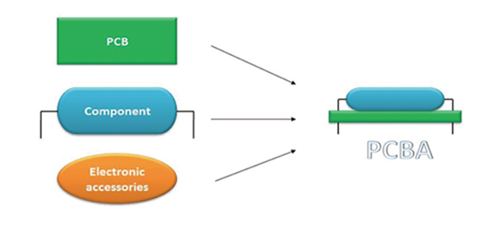
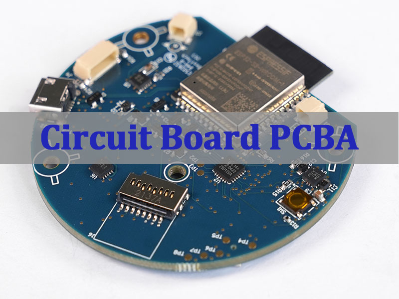
Circuit board PCBA means a finished Printed Circuit Board Assembly where components are sourced, placed, soldered, inspected, and tested to deliver a functional circuit board ready for integration into your product. This article explains how circuit board PCBA differs from bare PCB fabrication, what the PCBA process and testing include, how to avoid misbuild and rework, what drives pricing, and why short lead time depends on disciplined engineering inputs and production control.

When your schedule is tight, what usually blocks a “fast†circuit board PCBA build from shipping on time?

  • Quotes look fast, but lead time expands once parts are confirmed as long-lead or unavailable.
  • Incomplete engineering data triggers back-and-forth that burns days before production even starts.
  • The SMT line becomes the bottleneck when setup, stencil, or program readiness is late.
  • Hidden rework loops appear after first build due to unclear polarity, footprint, or assembly notes.
  • Testing is treated as an afterthought, so failures show up late and force retest or rebuild.

A circuit board PCBA manufacturer with short lead time removes these blockers by front-loading engineering clarity and locking a repeatable execution path.

  • Validate BOM availability and alternates early to prevent material-driven delays.
  • Standardize the engineering package so programs can be released without churn.
  • Pre-stage SMT readiness (stencil, feeders, programs) to keep the PCBA SMT schedule predictable.
  • Use risk-based inspections to catch defects before they become rework cycles.
  • Define PCBA testing requirements up front and ship with measurable test evidence.

EBest Circuit (Best Technology) is a PCB and PCBA manufacturer built for speed without sacrificing control. We combine in-house PCB fabrication and PCBA assembly, disciplined DFM review, component sourcing through an established supply network, and digital traceability that helps teams track lots, progress, and build status with high responsiveness. If you need a fast, stable circuit board PCBA build, contact sales@bestpcbs.com.

Circuit Board PCBA

How Does Printed Circuit Board Assembly PCBA Differ From Bare PCB Fabrication?

Bare PCB fabrication delivers the board structure; printed circuit board assembly PCBA delivers a working electronic assembly. For short lead time, the key difference is that PCBA adds supply chain and process dependencies that must be planned, not guessed.

What Changes When You Move From PCB To PCBA

  • Input Files Expand: PCBA needs BOM, Pick-and-Place, assembly drawings, and test requirements, not just Gerber.
  • Material Risk Appears: Availability, alternates, and minimum order quantities can control schedule.
  • Process Windows Matter: Paste type, reflow profile, and handling rules affect yield.
  • Inspection Becomes Mandatory: AOI/X-Ray strategy determines how early defects are caught.
  • Testing Defines “Doneâ€: Functional pass criteria must be agreed before shipping.

Quick Comparison Table

ItemBare PCB FabricationPrinted Circuit Board Assembly PCBA
DeliverableBoard StructureWorking Assembly
Main ConstraintsStack-Up, Drilling, FinishParts, SMT Setup, Yield, Test
Typical RisksLayer Registration, ImpedanceShortages, Misbuild, Rework
Lead Time DriverPanel ScheduleParts + SMT + Testing

Short lead time is easier to achieve in PCBA when the assembly scope and acceptance criteria are defined as clearly as the PCB build notes.

Circuit Board PCBA

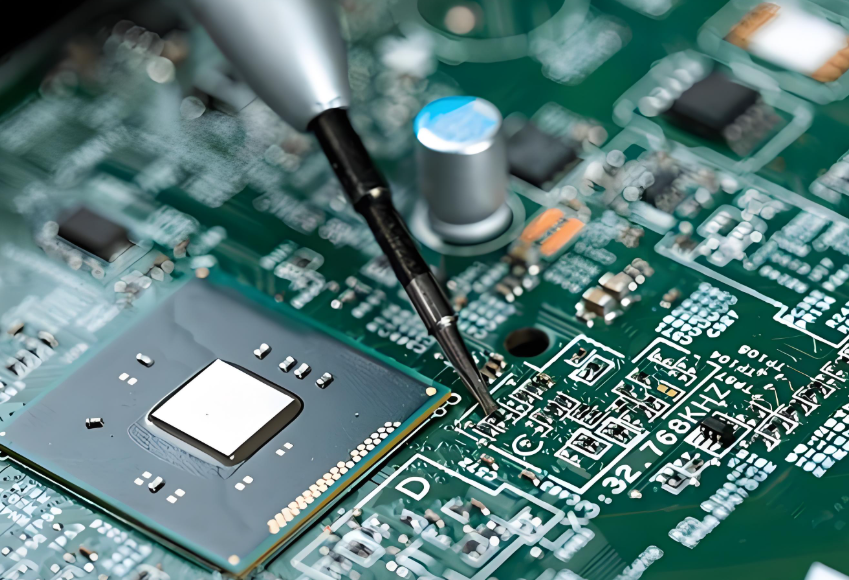
What Does The PCBA Process Include From SMT To Final Testing?

The PCBA process is a chain of controlled steps. For a short lead time build, the fastest programs are those where each step has clear inputs, defined checkpoints, and minimal iteration.

Typical PCBA Process Stages

  • Engineering Release: File validation, DFM, and build readiness checks.
  • Material Preparation: Kitting, baking (as needed), and ESD/Moisture controls.
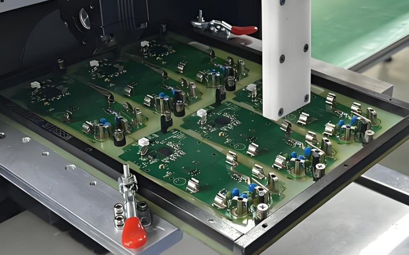
  • SMT PCBA Setup: Stencil, program, feeders, and first article verification.
  • Reflow And Inspection: Controlled profiling and AOI verification.
  • THT Or Secondary Ops: Through-hole, selective soldering, or hand solder.
  • Cleaning And Coating (If Required): Application-specific requirements.
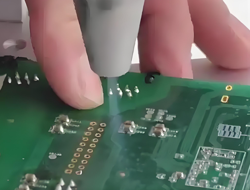
  • PCBA Testing: Functional testing, programming, and final verification.

What Accelerates The Process In Real Builds

  • Pre-approved alternates for common shortage items
  • Clear polarity and reference designators in assembly drawings
  • Defined test method and pass/fail rules before build starts
  • Stable revision control to avoid last-minute ECO churn

A short lead time circuit board PCBA build is not “rushing.†It is eliminating rework loops by making the process deterministic.

Why Is Qi Wireless Charger PCBA Circuit Board Design Critical For Charging Performance?

Qi wireless charger PCBA circuit board performance depends on how the electronics, coil, and mechanical constraints interact. Even if you are outsourcing assembly, design choices determine yield and functional pass rate, which directly affects lead time.

Design Elements That Influence Performance And Build Success

  • Coil Alignment Tolerance: Small alignment drift can reduce coupling efficiency.
  • Thermal Management: Power stages need controlled heat paths to avoid throttling.
  • EMI Layout Discipline: Switching noise can disrupt control loops and certification.
  • Component Selection: Key ICs and power components often have supply constraints.
  • Test Access: Pads and fixtures must support stable programming and validation.

Practical Note For Short Lead Time

If your Qi wireless charger PCBA circuit board coil supply is tight, lead time is often determined by coil procurement and incoming verification rather than by the SMT line speed.

For Qi builds, short lead time comes from aligning design-for-assembly, supply reality, and testability early, not from compressing the assembly window.

What Engineering Data Must Be Defined Before Starting A Circuit Board PCBA Build?

Fast builds start with complete, unambiguous engineering data. Missing or conflicting details usually create the longest delays because they pause the release process.

The Minimum Engineering Package For Speed

  • Gerber And Fabrication Notes: Stack-up, finish, thickness, impedance needs.
  • BOM With Manufacturer Part Numbers: Include alternates and do-not-substitute flags.
  • Pick-and-Place File: Centroid, rotation, and side designation.
  • Assembly Drawing: Polarity, special instructions, torque, and labeling needs.
  • Programming And Test Requirements: Test points, firmware, and pass criteria.
  • Revision Control: Clear version naming across all files.

A Simple Rule That Saves Days

If two files disagree, production stops. The fastest path is a single “source of truth†package.

A circuit board PCBA manufacturer with short lead time can only move as fast as the engineering package allows.

How Do Printed Circuit Board PCBA Services Reduce Rework And Misbuild Risk?

Good printed circuit board PCBA services reduce rework by preventing ambiguity and catching defects early. Rework is the silent lead time killer because it consumes capacity and forces retest.

What Reduces Misbuild Risk Most Effectively

  • DFM And DFA Review: Identify footprint, spacing, and assembly hazards before build.
  • BOM Risk Screening: Flag EOL, long-lead, and counterfeit-prone parts.
  • First Article Control: Validate placement, polarity, and orientation before full run.
  • Process Checkpoints: SPI (if used), AOI, and controlled reflow profiling.
  • Clear Work Instructions: Special notes for connectors, shielding, or sensitive parts.

Compact “Rework Cost†View

Rework Impact = (Rework Time × Line Rate) + Retest Time + Schedule Slip

Reducing rework is often the fastest and cheapest way to protect lead time.

PCBA services create speed by minimizing preventable mistakes, not by compressing inspection.

What Cost Drivers Actually Determine Printed Circuit Board PCBA Pricing?

Printed circuit board PCBA pricing is mainly determined by material strategy, assembly complexity, and testing scope. Fast builds can be cost-effective, but only if the program avoids last-minute changes and rework.

Primary Pricing Drivers

  • BOM Cost And Availability: Supply volatility and alternates affect price stability.
  • Placement Count And Mix: More placements and diverse packages increase cycle time.
  • Setup And NRE: Stencils, programming, and fixture preparation.
  • Double-Sided Or Fine-Pitch Requirements: Adds process and inspection time.
  • Testing Depth: Functional testing, programming, burn-in, or coverage requirements.
  • Yield Expectations: Tight yield targets require stricter process control.

Short Table For Quick Buyer Decisions

DriverHow It Moves CostHow It Moves Lead Time
BOM RiskHigher when scarceHigher when parts slip
Testing ScopeHigher with fixturesLonger when undefined
ComplexityHigher with fine pitchLonger with rework

Accurate pricing comes from defined scope. “Fast†quotes become expensive when assumptions are left unstated.

When Does SMT PCBA Become A Bottleneck In Volume Circuit Board Production?

In volume builds, SMT PCBA becomes the bottleneck when capacity is not the limiting factor—readiness is. The line can run quickly, but only if programs, materials, and change control are stable.

Common Bottleneck Triggers

  • Late Material Kitting: Missing a few critical parts stalls the entire line.
  • Program Instability: Frequent ECOs force revalidation and reset schedules.
  • Feeder And Setup Complexity: High-mix builds increase changeover time.
  • Stencil And Tooling Delays: Stencils and fixtures not ready on time.
  • Quality Hold Cycles: Unclear defect ownership slows release.

Practical Volume Tip

If you want short lead time at volume, lock a stable BOM and revision cadence. Change control discipline is often worth more than extra SMT capacity.

SMT PCBA bottlenecks are usually planning and release bottlenecks in disguise.

What Testing Methods Are Commonly Used In PCBA Printed Circuit Board Assembly?

PCBA testing should be chosen based on risk, volume, and failure impact. The wrong approach either adds cost with little value or misses defects until late, which breaks short lead time goals.

Common PCBA Testing Methods

  • Visual Inspection And AOI: Fast detection of solder and placement defects.
  • X-Ray Inspection (When Needed): For hidden joints like BGA.
  • In-Circuit Test (ICT): Strong for electrical opens/shorts in volume builds.
  • Flying Probe Test: Useful for lower volume without fixture investment.
  • Functional Test (FCT): Validates real-world operation and interfaces.
  • Programming And Calibration: Firmware loading and parameter checks.

Quick Test Selection Table

Build TypeTypical Best Fit
Prototype / Low VolumeFlying Probe + Functional Test
Medium VolumeAOI + Functional Test
High VolumeICT + Functional Test

Testing supports short lead time when it is defined early and matched to program risk, not added at the end as a rescue step.

To conclude, circuit board PCBA is the completed assembly that turns a bare PCB into a functional product-ready module, and its lead time is primarily controlled by engineering readiness, parts availability, SMT execution, and test definition.

This article explained how printed circuit board assembly PCBA differs from PCB fabrication, what the PCBA process includes, why Qi wireless charger PCBA circuit board design affects outcomes, how to reduce rework risk, what drives pricing, how SMT capacity becomes a bottleneck, and which PCBA testing methods fit different build scenarios.

EBest Circuit (Best Technology) supports short lead time builds through disciplined engineering review, in-house PCB and PCBA capability, and production control that keeps schedules predictable. For quotations or engineering review, pls feel free to contact us via sales@bestpcbs.com.

Circuit Board PCBA

FAQs

What is the difference between a circuit board and a PCBA?

A circuit board usually refers to a bare PCB, while a PCBA is the assembled version with components mounted and soldered, ready to function in a product.

What are common PCBA defects?

Common PCBA defects include solder bridges, insufficient solder, tombstoning, misalignment, wrong polarity, lifted leads, and intermittent connections caused by process variation.

How many types of PCBA are there?

PCBA is often categorized by assembly technology and complexity, such as SMT PCBA, through-hole PCBA, mixed-technology PCBA, single-sided, double-sided, and multilayer assemblies.

How Do Component Selection And Part Categories Affect Circuit Board PCBA Quote Accuracy?

Part categories influence whether components are readily available, require special sourcing, or create added handling and setup steps; these factors can change both cost and lead time if not defined in the quote assumptions.

What is the Meaning of PCBA? PCBA Process
Tuesday, April 8th, 2025

What Does the PCBA Stand For?

PCBA stands for Printed Circuit Board Assembly.

It’s a complete board where all parts are mounted and ready to work. The bare board itself is called a PCB. But once components like resistors, capacitors, and chips are soldered onto it, it becomes a PCBA. Sometimes, some electronic accessories will be soldered onto the PCB surface as well.

What is the Meaning of PCBA? PCBA Process

Key Components in PCBA

The value of a PCBA comes from the components it carries. Each part plays a role in how the circuit works. Let’s go over some of the most common parts:

  • Resistors: Control the flow of current.
  • Capacitors: Store and release energy when needed.
  • Inductors: Manage signals, especially in filters.
  • Diodes: Let current flow in one direction only.
  • Transistors: Switch or amplify signals.
  • ICs (Integrated Circuits): Small chips with many tiny parts inside. They perform complex functions.
  • Connectors: Help connect the board with other systems.
  • Transformers: Change voltage levels for safer or better operation.
What is the Meaning of PCBA? PCBA Process

All these parts must be carefully chosen and placed. A small mistake can stop the board from working right. That’s why design and assembly matter so much.

Types of PCBA Assembly Techniques

1. Surface Mount Technology (SMT)

This is the most common method today. Components are placed directly on the surface of the board. Pick and place machines handle most of the work, which keeps it fast and accurate. SMT supports miniaturized parts and high-speed production.

2. Through-Hole Technology (THT)

This technique uses components with leads that go through holes in the PCB. These leads are soldered on the other side. THT is strong and used for large or high-stress parts like connectors or transformers.

3. Mixed Technology Assembly

Some boards use both SMT and THT. Surface-mount parts go on first, then through-hole components are added by manually. This mix allows for flexible, compact, and reliable designs.

What is the difference in PCB and PCBA?

Though the terms PCB and PCBA are often used together, they describe very different stages in the electronics manufacturing process. And you must to know: PCB are one of important part of PCBA, but PCBA not. Below we listing the key differences between them:

FactorPCBPCBA
StageBlank boardAssembled with components
ComponentsNoYES
FunctionalityNon-functionalFully operational
Manufacturing CostLowHigher (because include the components cost)
TestingBasic inspectionComplete electrical testing
Assembly TechniquesNot applicableSMT, THT, or hybrid
Files NeededGerber, drill filesGerber, BOM, pick & place, assembly files
Lead Time (under same design)ShortRelated longer than PCB

What Is the Use of PCBA?

PCBAs are used in almost everything you see around:

  • Phones: Control your screen, camera, and sound.
  • Computers: Process data, run programs.
  • Vehicles: Support GPS, safety features, engine control.
  • Medical devices: Power equipment like MRI or ECG machines.
  • Home appliances: From smart TVs to microwave ovens.

Without a PCBA, none of these would work. It’s like the brain of any electronic device. From simple tools to high-end gadgets, PCBA plays a big role.

How to Do PCBA Testing?

Testing makes sure the board works as expected. It helps catch issues before the board goes into the final product. There are several ways to test a PCBA:

1. Visual Inspection

This is the first step. Technicians or machines check if parts are in the right place. They also look for bad solder joints, cracks, or missing items.

2. Automated Optical Inspection (AOI)

AOI mainly uses a camera system scans the board. It checks for incorrect or misaligned parts. It’s faster than manual inspection and works well for large batches.

3. In-Circuit Testing (ICT)

ICT checks each component directly. It makes sure resistors, capacitors, and connections work properly.

4. Functional Testing

This test powers the board and simulates how it will be used. It checks whether the PCBA can perform the expected tasks.

5. X-Ray Inspection

Used when components are hard to see, like BGAs (Ball Grid Arrays). The X-ray looks through the board to catch hidden problems.

6. Flying Probe Test

For small batches, probes test different points without a custom fixture. It’s flexible and cost-effective.

7. Testing with jig

This is used for mass production, jig tools are made according to the design files, so it is a customized. Jig testing can save much time compared with flying probe.

EBest Circuit (Best Technology) deeply know the importance of the product quality, so we pay more attention to the PCB board quality checking process. We set a QC department according to ISO9001:2015 and ensure all processes are compliance with quality system.

How Do You Clean a PCBA?

During the PCB assembly process, cleaning a PCBA is an important step, especially after soldering. Residual flux, dust, or moisture can affect the performance of the board. Nowadays, the common cleaning methods used in EBest Circuit (Best Technology) are:

1. Manual Cleaning

This is the most basic method. A technician uses a soft anti-static brush and high-purity isopropyl alcohol to remove visible flux or dirt. It’s ideal for prototypes, small batches, or after rework or repair. Manual cleaning gives the operator control, especially in tight or delicate areas. However, it’s time-consuming and not suitable for large-scale production.

What is the Meaning of PCBA? PCBA Process

2. Ultrasonic Cleaning

Ultrasonic cleaning is widely used for complex boards and mass production. The PCBA is submerged in a tank filled with a cleaning solution. High-frequency sound waves pass through the liquid, creating microscopic bubbles. These bubbles collapse rapidly, producing a scrubbing action known as cavitation.

This technique reaches tiny gaps under components where brushes can’t go. It’s very effective for removing dried flux, fine dust, or ionic contamination. The process is gentle on components but powerful enough to clean even the most compact assemblies. After cleaning, the board is rinsed and dried with warm air or placed in a drying chamber.

What is the Meaning of PCBA? PCBA Process

3. Dry Ice Cleaning

Dry ice cleaning is a newer, eco-friendly technique. It uses solid COâ‚‚ pellets, also called dry ice, blasted at high speed onto the PCBA surface. As the pellets hit, they turn into gas instantly. This process lifts off dirt, flux, and even adhesives without leaving moisture or residue behind.

What is the Meaning of PCBA? PCBA Process

Dry ice cleaning works well for delicate electronics and is especially useful in industries where cleanliness must meet strict standards. To give customer a highest quality of the PCBA, our SMT factory equipped with the dry ice cleaning machine to ensure a clear surface while improve the efficiency.

PCBA Assembly Process

The PCBA assembly process is relatively simple than PCB manufacturing, actually the most tedious step is to load all the components on the pick and place machine, and set the program parameters. Here we break down all the processes of the mass production PCB assembly, from the solder paste printing to function testing.

1. Solder Paste Printing

First, solder paste is applied to the bare PCB. This paste is mainly consists of silver and tin, a mix of tiny solder particles and flux. A stencil is placed over the board, and the paste is spread across it using a squeegee. The paste sticks only to the exposed pads where components will be mounted.

2. Load components feeder

Load all the components in the feeder of the pick and place machines, make sure all the parameter of components are correct, and double check the direction of chips. It is a simple but tedious step and need much time to check everything is okay. 

2. Pick and Place

After applying solder paste, automated pick-and-place machines begin placing surface-mount components onto the board. These machines work fast and accurately. They follow a file created during PCB design that tells them the exact location for each part. The components sit on the solder paste, which holds them in place temporarily.

3. Reflow Soldering

Next, the assembled board goes through a reflow oven. The oven slowly heats the board in stages. When it reaches a high enough temperature, the solder paste melts and forms strong electrical and mechanical connections between the parts and the board. After this, the board cools down, and the solder solidifies.

This step is only for SMT components. If the board has only through-hole parts, this step may be skipped.

4. Inspection (AOI and Visual)

Once the soldering is done, the board goes through inspection. Automatic Optical Inspection (AOI) machines scan the board using high-resolution cameras. They check for misaligned parts, soldering problems, or missing components. For small production or sensitive areas, manual inspection is also performed to catch anything machines might miss.

5. Through-Hole Component Insertion (If Needed)

If the board uses through-hole technology (THT), this is when those parts are added. Workers or machines insert the components into the holes, and the leads go through to the other side of the board. These components are often bulkier, like connectors or transformers.

6. Wave Soldering (For THT)

For boards with many through-hole parts, wave soldering is used. The board passes over a wave of molten solder that touches the underside. This solders all the leads at once. It’s fast and effective, especially for high-volume production. For small-scale or sensitive boards, hand soldering might be used instead.

7. Final Inspection and Quality Control

After soldering, the entire board is checked again. Technicians or AOI machines inspect the final assembly. They look for cold joints, excess solder, or misplaced parts. Boards may also be tested with X-ray machines to inspect solder joints under BGAs or hidden areas.

8. Functional Testing (FCT)

The next step is functional testing. The board is powered up and tested to make sure it works correctly. This could include checking voltages, signals, response times, and communication with other devices. Engineers may use test jigs or test programs based on the end application.

9. Cleaning (If Needed)

After all soldering and testing, the board might be cleaned to remove flux residue. Depending on the flux used, this could be manual, ultrasonic, or dry ice cleaning. Clean boards are especially important in high-reliability fields like aerospace, automotive, or medical.

10. Conformal Coating or Protection (Optional)

For some applications, a conformal coating is applied. This is a protective layer that shields the board from moisture, dust, and chemicals. It’s often used in harsh environments. Coating can be applied by spraying, dipping, or brushing.

11. Packaging and Shipping

Finally, once the PCBA passes all checks, it’s packed carefully. Anti-static bags, foam, and trays protect it during transport. Labels are added for tracking and traceability. From here, it’s ready to be installed into the final product. Here is a whole process of pcb assembly in EBest Circuit (Best Technology).

PCBA HS Code

Every product for trade needs a code. The HS code for PCBA usually is 8517799000

But depending on the use or market, some customs may use a different classification. For example:

853400 for bare board parts, sometimes be used on certain assembled parts.

847330 for boards used in computers.

853710 for board which used as controller or controller unit.

Noted: Always check with your country’s customs for the right code. Using the wrong one may cause delays or extra costs.

Our PCBA Services

At EBest Circuit (Best Technology), we specialize in end-to-end PCBA services. From design to delivery, we support your project with speed, quality, and reliability. We can be your first choice because:

  1. We have 18+ years in PCB industry
  2. One-Stop Service: PCB fabrication, parts sourcing, SMT/THT assembly, testing
  3. Custom Solutions: From prototypes to mass production, no MOQ
  4. Skilled Engineers: For DFM & DFA checks and process optimization
  5. Strict Quality Control: 9-times QC check, including AOI, X-ray, ICT, and functional testing
  6. Global Delivery: Fast and on time, wherever you are
  7. Component Sourcing: Only original, trusted parts, we have cooperated with digikey, findchips, mouser for over 10 years, and we can get the most competitive price from them.
  8. PCB Fabrication: Rigid, flex, metal-core, ceramic, and more.

Whether you’re working on a simple control board or a multi-layer high-speed system, we’re here to support you.